5G Infrastructure PCB mm Wave Antennas Low Loss
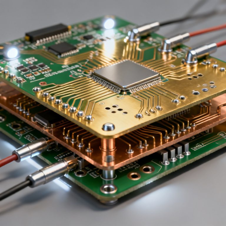
5G Infrastructure PCB design for mmWave antennas and low loss is critical for modern base stations and small cells, enabling high-frequency signal integrity and thermal reliability in demanding network environments.
Why 5G Infrastructure PCBs Are Different
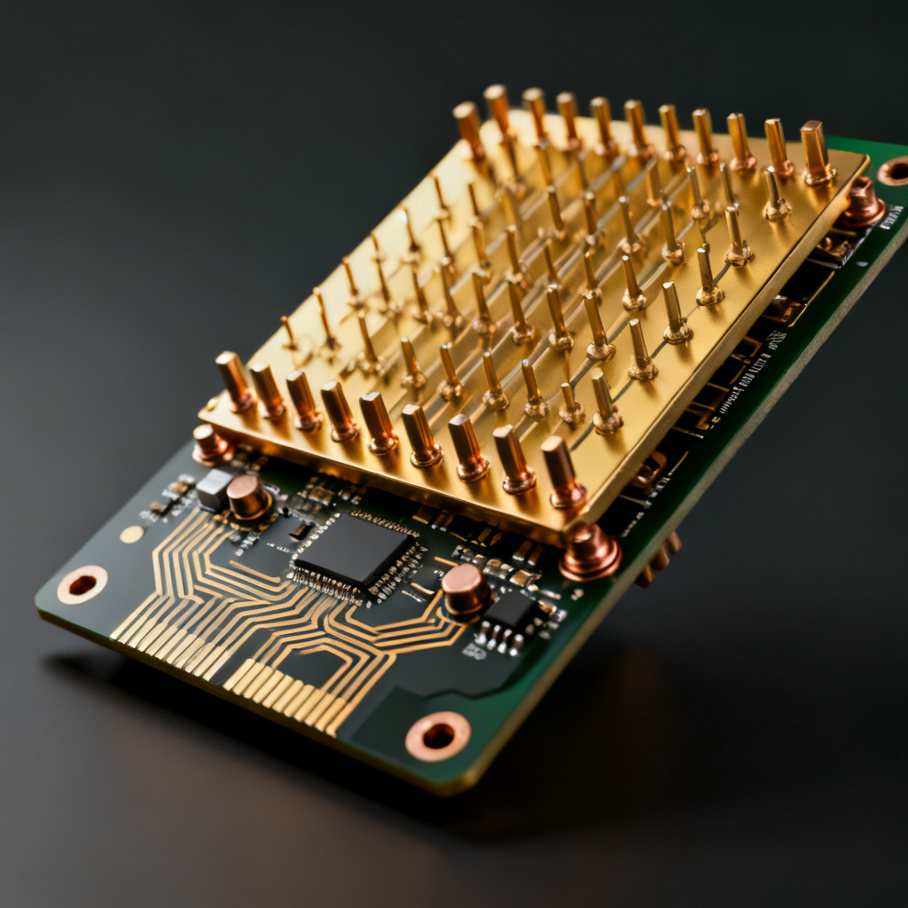
5G Infrastructure PCB requirements diverge sharply from 4G/LTE due to mmWave frequencies. Traditional FR-4 laminates, cost-effective for sub-1 GHz, exhibit unacceptable dielectric loss above 1 GHz. For 5G mmWave applications, this loss becomes a bottleneck. The primary challenge is dielectric loss (dissipation factor, Df) and conductor loss (skin effect). At mmWave frequencies, signals travel on the surface of copper traces, requiring smoother copper foils and advanced laminates. Thermal management is critical: base stations generate substantial heat from high-power amplifiers, and PCB materials must have a high glass transition temperature (Tg) and low coefficient of thermal expansion (CTE) to prevent warpage and delamination. Consistent dielectric constant (Dk) across the board is essential, as any variation can detune antennas and degrade beamforming performance.
Material Selection for Low-Loss mmWave PCBs
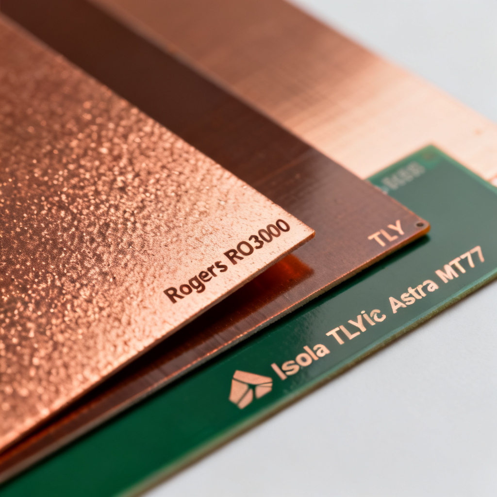
The choice of PCB laminate is the single most important factor for 5G Infrastructure PCB performance. PTFE (polytetrafluoroethylene)-based composites, such as Rogers RO3000 series or Taconic TLY series, offer Df as low as 0.001 to 0.002 at 10 GHz. These materials maintain stable Dk (2.2 to 3.0) across wide temperature and frequency ranges. Ceramic-filled hydrocarbon laminates, like Rogers RO4000 series or Isola Astra MT77, are popular for their lower cost and compatibility with standard FR-4 processing, though they have slightly higher Df (0.002 to 0.003). For hybrid boards (mixing FR-4 with high-frequency laminates), the transition zone must be carefully designed to avoid impedance mismatches. Copper foil roughness (RMS < 1.0 µm) is essential; electrodeposited (ED) foil with reverse treatment (RTF) or rolled annealed (RA) foil minimizes conductor loss.
Key Material Parameters for 5G Infrastructure PCB
| Parameter | Requirement for 5G Infrastructure PCB | Impact on mmWave Antennas |
|---|---|---|
| Dissipation Factor (Df) | < 0.002 at 10 GHz | Reduces dielectric loss, improves antenna efficiency |
| Dielectric Constant (Dk) | 2.2–3.0, stable across frequency | Ensures impedance consistency for antenna arrays |
| Copper Surface Roughness | < 0.5 µm RMS | Minimizes conductor loss at mmWave frequencies |
| Glass Transition Temperature (Tg) | > 280°C | Prevents warpage during high-power operation |
| Moisture Absorption | < 0.02% | Maintains stable Dk in humid environments |
mmWave Antenna Design on PCBs
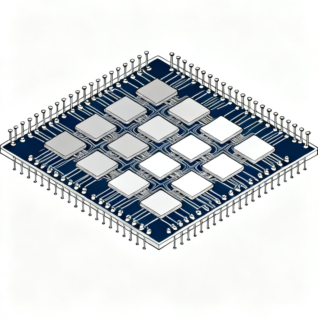
5G Infrastructure PCB antenna design for mmWave uses phased array antennas for beamforming, requiring multiple radiating elements (patches, dipoles, or slots) etched directly onto the board. The antenna element spacing must be less than half the wavelength (e.g., < 6 mm at 28 GHz) to avoid grating lobes. This demands tight tolerances on etching (line/space width ±0.025 mm) and layer registration (±0.05 mm). The feed network (microstrip lines, striplines, or coplanar waveguides) must use impedance-controlled transmission lines, typically 50 ohms, with via fences or ground planes to suppress parasitic radiation. Antenna-in-package (AiP) using multi-layer PCBs with embedded antennas reduces interconnect loss and simplifies assembly. For high-gain applications, substrate-integrated waveguide (SIW) structures offer low loss and high isolation.
Critical Design Considerations for mmWave Antenna PCB
- Dielectric Loss: Select materials with Df < 0.002 for optimal 5G Infrastructure PCB performance. Even a 0.001 difference can result in 0.1 dB/cm loss at 28 GHz.
- Conductor Loss: Use thicker copper (1 oz to 2 oz) for power traces but thinner copper (0.5 oz) for signal traces to reduce skin effect. Copper surface roughness should be < 0.5 µm RMS.
- Impedance Control: Impedance tolerance must be ±5% or better, requiring precise control of trace width, dielectric thickness, and Dk. Use 2D or 3D field solvers (e.g., Ansys HFSS, CST) for simulation.
- Via Design: Stub vias cause resonance and reflections. Use back-drilling to remove unused via stubs, reducing insertion loss by up to 0.2 dB per via. Microvias (laser-drilled, < 0.15 mm diameter) are preferred for high-density interconnects.
- Surface Finish: ENIG (electroless nickel immersion gold) is standard, but immersion silver (ImAg) offers lower loss at mmWave. Avoid HASL (hot air solder leveling) due to uneven surfaces.
Manufacturing Challenges for 5G Infrastructure PCBs
Producing reliable 5G Infrastructure PCB requires advanced fabrication capabilities. Laser direct imaging (LDI) is mandatory for fine-line etching (down to 0.075 mm line/space). Lamination pressure and temperature must be tightly controlled for PTFE materials, which can be soft and prone to flow. Controlled impedance testing (TDR, time-domain reflectometry) is essential for every panel, with a pass/fail criterion of ±5% from the target impedance. For hybrid boards, the bonding of dissimilar materials (e.g., PTFE to FR-4) requires specialized prepregs (e.g., Rogers 2929 bondply) to prevent delamination.

Thermal Management and Reliability
5G Infrastructure PCB reliability for base stations operating in harsh outdoor environments (-40°C to +85°C) demands materials with a CTE (in the Z-axis) below 50 ppm/°C to prevent via barrel cracking. Use thermal vias (filled with copper or thermally conductive epoxy) under high-power components to dissipate heat. Accelerated life testing (thermal cycling, humidity bias) is critical to validate long-term reliability. For mmWave antennas, any moisture absorption (e.g., > 0.1%) can shift Dk and detune the antenna; thus, materials with low moisture absorption (< 0.02%) are preferred.
Testing and Validation
To ensure performance, every 5G Infrastructure PCB must undergo rigorous testing:
- Impedance Testing: TDR for single-ended and differential traces.
- Insertion Loss Measurement: Using vector network analyzers (VNA) up to 110 GHz.
- Antenna Pattern Measurement: In an anechoic chamber to verify gain, side lobe levels, and beamwidth.
- Thermal Imaging: To detect hot spots from high-power RF circuits.
- Microsectioning: To verify via integrity and layer registration.
Why Choose Us for Your 5G Infrastructure PCBs
As a professional B2B PCB manufacturer specializing in high-frequency and high-reliability boards, we offer:
- Material Expertise: We work with all major low-loss laminates (Rogers, Taconic, Isola, Nelco) and can source custom materials for unique Dk/Df requirements.
- Advanced Capabilities: LDI for fine lines (0.05 mm), laser drilling for microvias (0.1 mm), back-drilling for via stubs, and controlled impedance testing.
- Hybrid Board Fabrication: Seamless integration of PTFE and FR-4 layers using optimized bonding processes.
- Quality Assurance: ISO 9001, UL 94V-0, and IPC-6012 Class 3 certified. 100% electrical testing and thermal cycling for every order.
- Fast Turnaround: Prototypes in 5-7 days, production in 2-3 weeks.
Contact us today for a quote on your next 5G Infrastructure PCB project. Let our engineering team help you select the right materials and design for mmWave antennas and low-loss performance.
Frequently Asked Questions About 5G Infrastructure PCB
What is the best material for 5G Infrastructure PCB?
For 5G Infrastructure PCB, PTFE-based laminates like Rogers RO3000 series offer the lowest loss for mmWave antennas, with Df as low as 0.001 at 10 GHz.
How does low loss affect 5G Infrastructure PCB performance?
Low loss in 5G Infrastructure PCB ensures minimal signal attenuation at mmWave frequencies, directly improving antenna gain and overall system efficiency.
What are common challenges in 5G Infrastructure PCB manufacturing?
Key challenges include maintaining tight impedance control, managing thermal expansion, and ensuring reliable bonding in hybrid stackups for 5G Infrastructure PCB.
Why is impedance control critical for mmWave antennas on 5G Infrastructure PCB?
Impedance control ensures consistent signal integrity across the antenna feed network, preventing reflections that degrade beamforming in 5G Infrastructure PCB designs.