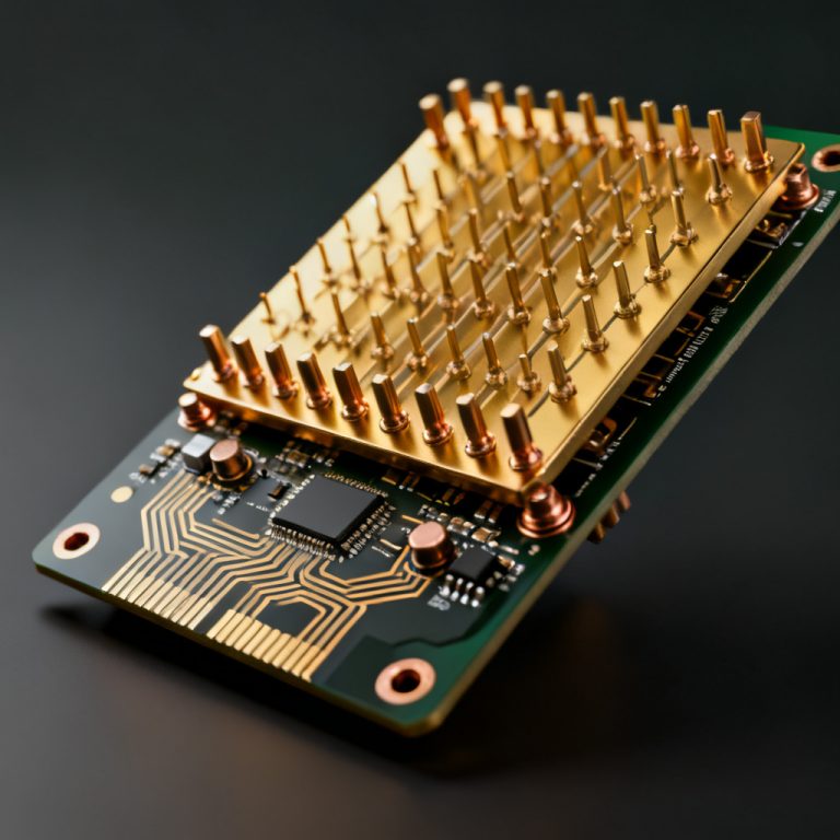
Specialty PCB Guide Ceramic Embedded Components
This comprehensive Specialty PCB Guide Ceramic Embedded Components manual delivers advanced board selection rules for high-temperature and high-frequency hardware packaging.
In the rapidly evolving world of electronics, standard FR4 PCBs often fall short in meeting the demands of high-frequency, high-temperature, or miniaturized applications. This is where specialty PCBs—particularly ceramic PCBs and embedded component PCBs—come into play. These advanced technologies enable superior thermal management, signal integrity, and space efficiency, making them indispensable for industries like aerospace, automotive, medical devices, and telecommunications.
This comprehensive guide merges insights from the top three authoritative sources on specialty PCBs, providing you with a deep dive into the materials, design considerations, manufacturing processes, and applications of ceramic and embedded component PCBs. Whether you are an engineer, procurement specialist, or business owner, this pillar content will equip you with the knowledge to make informed decisions for your next high-performance PCB project.
Part 1: Ceramic PCBs – The Foundation of High-Temperature and High-Frequency Performance
1.1 What Are Ceramic PCBs?
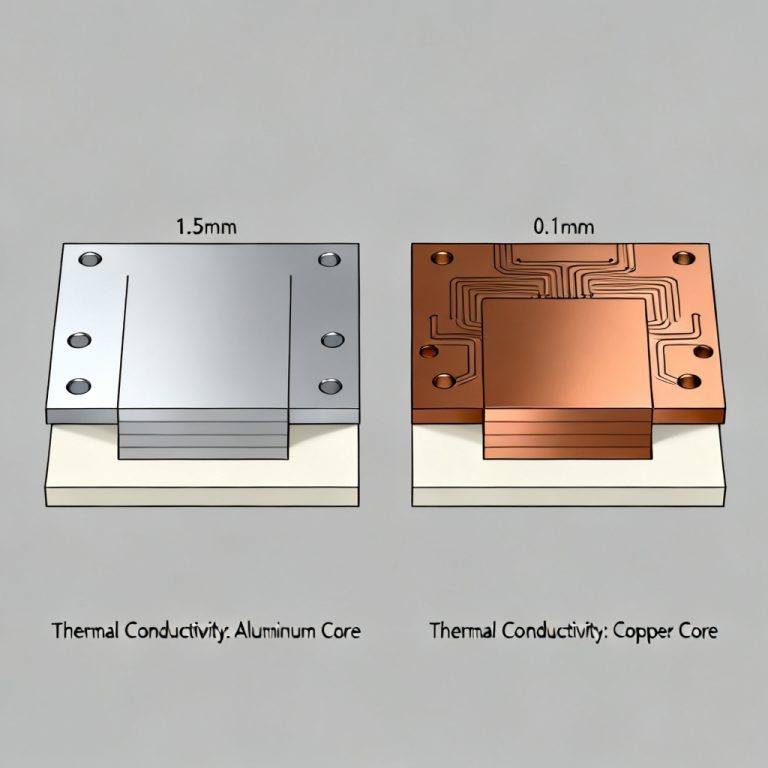
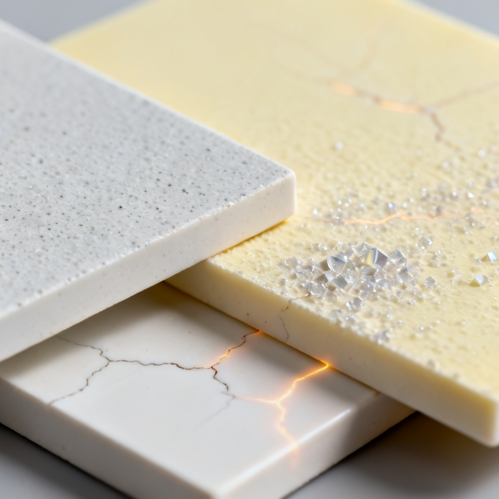
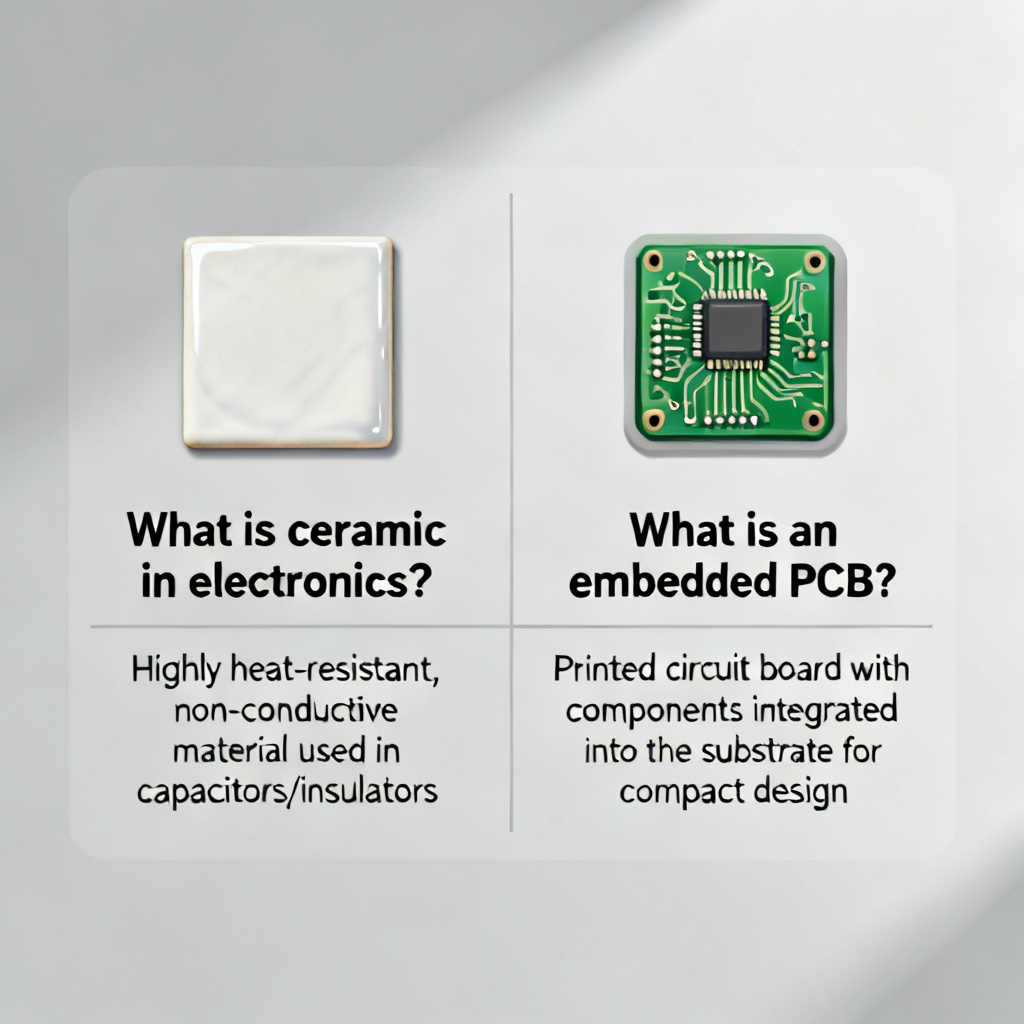
Ceramic PCBs are printed circuit boards that use a ceramic-based substrate instead of traditional FR4 (fiberglass epoxy) or other organic materials. Common ceramic substrates include alumina (Al₂O₃), aluminum nitride (AlN), and beryllium oxide (BeO). These materials offer superior thermal conductivity, electrical insulation, and mechanical stability, making them ideal for demanding environments.
1.2 Key Properties of Ceramic Substrates
| Material | Thermal Conductivity (W/m·K) | Dielectric Constant (at 1 MHz) | Typical Applications |
|---|---|---|---|
| Alumina (96%) | 20-30 | 9.8 | General-purpose high-temp, LED, power modules |
| Aluminum Nitride | 170-200 | 8.8 | High-power RF, IGBT modules, automotive |
| Beryllium Oxide | 250-300 | 6.8 | Military, aerospace (handled with caution due to toxicity) |
Ceramic PCB thermal management: dissipates heat 5-10 times better than FR4, reducing component failure risk. CTE matching with silicon chips minimizes stress during thermal cycling. High-frequency performance: low dielectric loss and stable dielectric constant ensure signal integrity in RF and microwave applications.
1.3 Types of Ceramic PCB Manufacturing Technologies
1.3.1 Thick-Film Ceramic PCBs
Conductive pastes (e.g., silver, gold) are screen-printed onto a ceramic substrate and fired at 850-1000°C. Cost-effective for low-volume, high-reliability circuits; excellent adhesion; suitable for multilayer up to 8 layers. Limitations: line width/spacing typically >100 μm, lower conductivity compared to copper.
1.3.2 Thin-Film Ceramic PCBs
Thin metal layer deposited via sputtering or evaporation, patterned using photolithography. High precision (line widths down to 10 μm), excellent surface smoothness for high-frequency circuits. Applications: microwave circuits, medical sensors, optical communication modules.
1.3.3 Direct Bonded Copper (DBC) Ceramic PCBs
Copper sheet directly bonded to ceramic substrate (alumina or AlN) at high temperature. High current-carrying capacity (up to 100 A), excellent thermal conductivity, robust mechanical bond. Applications: power electronics, IGBT modules, LED lighting.
1.3.4 LTCC (Low-Temperature Co-fired Ceramic)
Multiple layers of unfired ceramic tape laminated with conductive pastes, co-fired at 850-900°C. True 3D integration of passive components within the substrate; hermetic sealing. Applications: RF modules, automotive radar, implantable medical devices.
1.4 Design Considerations for Ceramic PCBs
Substrate thickness: typically 0.25 mm to 1.0 mm; thinner substrates improve heat transfer but require careful handling. Metalization adhesion: use appropriate surface preparation (e.g., plasma cleaning) to prevent delamination. Via filling: for multilayer ceramic PCBs, vias must be filled with conductive paste. Thermal vias: add arrays under high-power components. Solder mask: not always required; ceramic surfaces are naturally insulating.
1.5 Applications of Ceramic PCBs
LED Lighting: high-power LEDs use ceramic PCBs for efficient heat dissipation. Power Electronics: IGBT modules and DC-DC converters benefit from AlN substrates. RF and Microwave: radar systems and satellite communications rely on ceramic PCBs for low loss. Automotive: engine control units (ECUs) and battery management systems (BMS) withstand under-hood temperatures. Medical: implantable devices require biocompatible, hermetic ceramic substrates.
Part 2: Embedded Component PCBs – The Key to Miniaturization and Performance
2.1 What Are Embedded Component PCBs?
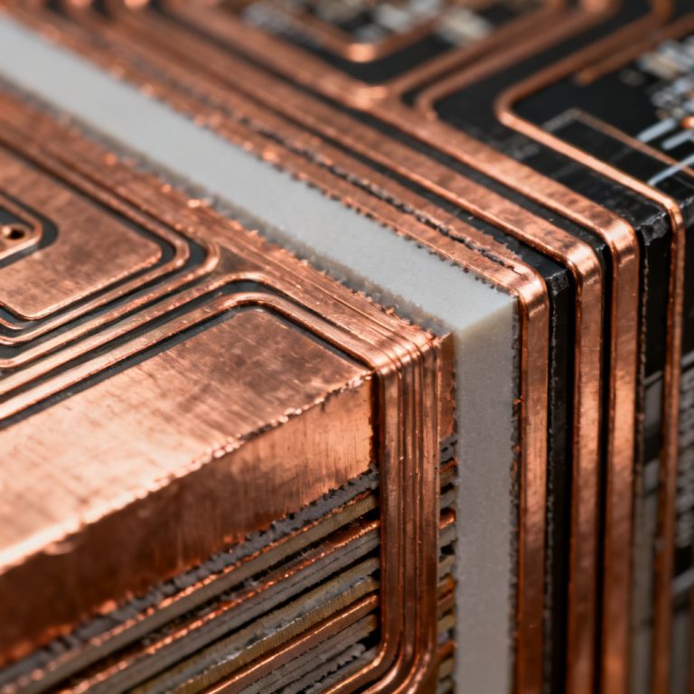
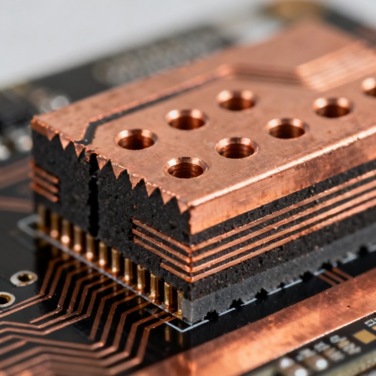
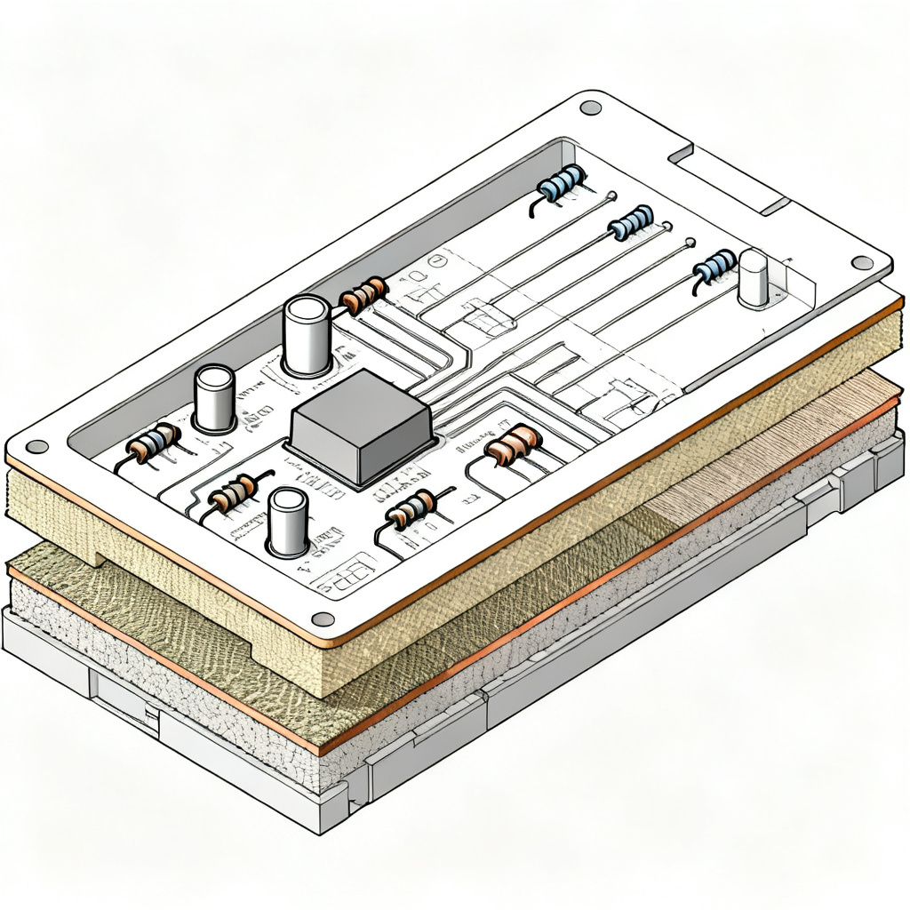
Embedded component PCBs integrate passive or active components directly into internal layers of the PCB substrate, rather than mounting them on the surface. This technology allows for significant space savings, reduced parasitic effects, and improved electrical performance.
2.2 Types of Embedded Components
Embedded Passive Components: resistors, capacitors, inductors fabricated using thin-film or thick-film processes within the PCB laminate. Embedded Active Components: bare dies embedded in cavities, interconnected using microvias or wire bonding. Embedded Substrates: multi-layer laminates with pre-embedded components from specialized suppliers.
2.3 Manufacturing Processes for Embedded Component PCBs
2.3.1 Lamination-Based Embedding
Components placed on a core layer, laminated with prepreg and copper foil. Laser drilling and plating create interconnections. Advantages: compatible with standard PCB fabrication; supports both passive and active components. Limitations: requires precise alignment and high-temperature/pressure lamination.
2.3.2 Cavity-Based Embedding
Cavity routed or laser-drilled into the PCB substrate, component inserted, cavity filled with dielectric material. Can handle larger components; allows for thermal management via exposed backside. Applications: power modules, RF front-end modules.
2.3.3 Laser Direct Structuring (LDS)
Laser activates a special additive in the molding compound, allowing selective copper plating to create circuitry directly on the component. Enables 3D circuit structures; suitable for highly miniaturized devices.
2.4 Design Considerations for Embedded Component PCBs
Component selection: use components rated for embedding (e.g., thin-film resistors, MLCC capacitors with high-temperature tolerance). Thermal management: use thermal vias or metal-core layers. Signal integrity: shorter interconnects reduce parasitic inductance and capacitance. Testing and repair: ensure thorough design validation before production. Layer stackup: plan to accommodate component thickness and ensure even copper distribution.
2.5 Benefits of Embedded Component PCBs
Space saving: reduces PCB area by up to 50%. Improved electrical performance: shorter signal paths reduce delay and crosstalk. Enhanced reliability: fewer solder joints reduce failure points. Cost reduction: in high-volume production, embedding lowers overall system cost.
2.6 Applications of Embedded Component PCBs
Smartphones and Wearables: embedded passives save space for batteries and sensors. IoT Devices: miniature sensors and transceivers benefit from reduced size. Medical Implants: embedded active components enable hermetic, ultra-compact designs. Automotive ADAS: radar modules use embedded components for high-frequency performance. Aerospace: avionics systems reduce weight and wiring complexity.
Part 3: Comparison and Selection Guide – Ceramic vs. Embedded Component PCBs
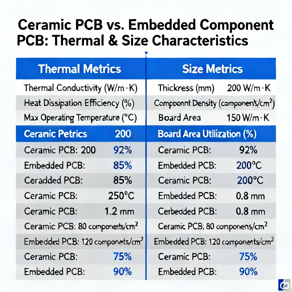
| Aspect | Ceramic PCBs | Embedded Component PCBs |
|---|---|---|
| Primary Benefit | Thermal management & high-frequency stability | Miniaturization & performance density |
| Typical Substrate | Alumina, AlN, BeO | Standard FR4, high-Tg laminates, or ceramic |
| Max Operating Temperature | Up to 350°C (AlN) | Typically up to 150°C (FR4) |
| Component Density | Medium (passive only) | High (passive + active) |
| Manufacturing Complexity | Moderate (specialized processes) | High (requires precision placement & lamination) |
| Cost per Unit Area | Higher (material cost) | Higher (process cost) |
| Best For | High-power, high-temp, RF | Ultra-compact, high-density, mixed-signal |
When to Choose Ceramic PCBs: operating temperature exceeds 150°C; high power dissipation; RF/microwave circuits requiring low dielectric loss; hermetic sealing. When to Choose Embedded Component PCBs: space is critical; need to reduce parasitic effects in high-speed digital circuits; high-volume production. Hybrid Approach: combine ceramic substrates with embedded components for ultimate performance, e.g., ceramic core with embedded power ICs for satellite transceivers.
Part 4: Manufacturing Considerations and Quality Assurance
4.1 Key Manufacturing Challenges
Ceramic PCBs: brittleness requires careful handling with diamond-tipped tools; sintering shrinkage must be compensated in design (12-16% for LTCC). Embedded Component PCBs: component placement accuracy within ±25 μm; lamination voids can cause delamination; use vacuum-assisted lamination.
4.2 Testing and Inspection
X-ray Inspection: essential for detecting voids in via fills, misaligned embedded components. Thermal Cycling: test boards under -55°C to +125°C for 500 cycles. Electrical Testing: fly-probe or fixture-based testing for continuity and isolation. Microsectioning: cross-section analysis to verify layer alignment.
4.3 Quality Standards
IPC-6012: rigid PCB qualification (applicable to ceramic PCBs). IPC-6013: flexible and rigid-flex PCBs (relevant for embedded component designs). MIL-PRF-31032: for military-grade ceramic PCBs. ISO 13485: for medical device PCBs.
Part 5: Future Trends in Specialty PCBs
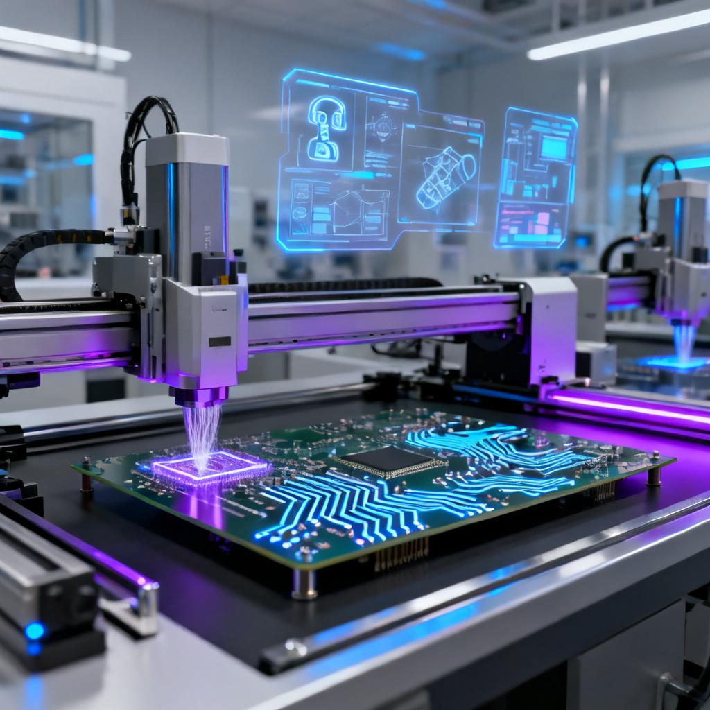
Additive Manufacturing: 3D printing of ceramic substrates and embedded circuits reduces lead time. High-Density Interconnect (HDI): microvias combined with embedded components for greater density. Advanced Materials: GaN and SiC power devices require PCBs with ultra-high thermal conductivity. Embedded Cooling: microfluidic channels within the PCB substrate for liquid cooling. AI-Driven Design: machine learning optimizes component placement and thermal via distribution.
Conclusion
Specialty PCBs—ceramic and embedded component technologies—represent the frontier of PCB innovation. Ceramic substrates excel in thermal and high-frequency performance, while embedded components enable unprecedented miniaturization and electrical efficiency. By understanding the material properties, design rules, and manufacturing processes outlined in this Specialty PCB Guide (Ceramic, Embedded Components), you can confidently select the right approach for your next project. For B2B procurement, partnering with a manufacturer that offers both capabilities is key. Our facility supports ceramic PCB production (alumina, AlN, LTCC) and embedded component integration under one roof, with rigorous quality control and fast turnaround. Contact our engineering team today to discuss your specialty PCB requirements.
Frequently Asked Questions (FAQ)
What is the main advantage of a ceramic PCB over FR4?
The main advantage of a ceramic PCB is its superior thermal conductivity and high-temperature stability, making it ideal for high-power and RF applications.
Can embedded component PCBs be repaired?
Embedded component PCBs are difficult to repair due to their integrated structure; thorough design validation is critical before production.
Which industries benefit most from specialty PCBs?
Industries like aerospace, automotive, medical devices, and telecommunications benefit most from ceramic and embedded component PCBs for their thermal management and miniaturization needs.
How do I choose between ceramic and embedded component PCBs?
Choose ceramic PCBs for high-temperature or high-frequency applications; choose embedded component PCBs for space-constrained or high-density designs.
What are the cost implications of specialty PCBs?
Specialty PCBs typically have higher material or process costs, but they can reduce overall system cost in high-volume or performance-critical applications.