Rigid PCB Guide Single Double Multilayer
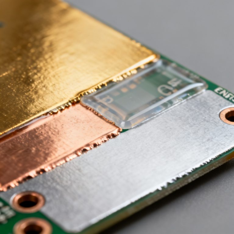
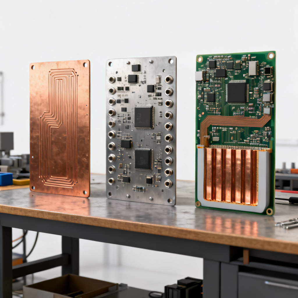
This comprehensive Rigid PCB Guide Single Double Multilayer manual serves as your definitive technical resource for understanding single-sided, double-sided, and multi-layer printed circuit boards. Whether you are a design engineer or a procurement specialist, this guide covers everything from stackup and materials to cost factors and applications.
- Single-Sided Rigid PCBs
- Double-Sided Rigid PCBs
- Multilayer Rigid PCBs
- Comparative Analysis
- How to Choose
- Manufacturing Process
- FAQ
What is a Rigid PCB? – The Foundation
Rigid PCBs are built on a solid, non-bendable substrate, typically FR-4 glass epoxy, providing a stable platform for mounting components. All rigid boards share these fundamental layers: substrate (core material), copper layer, solder mask, and silkscreen. Key physical properties include thickness (standard 1.6mm), copper weight (1 oz/ft² typical), and Tg (glass transition temperature, standard FR-4 at 130-140°C).
Single-Sided Rigid PCBs – The Cost-Effective Workhorse
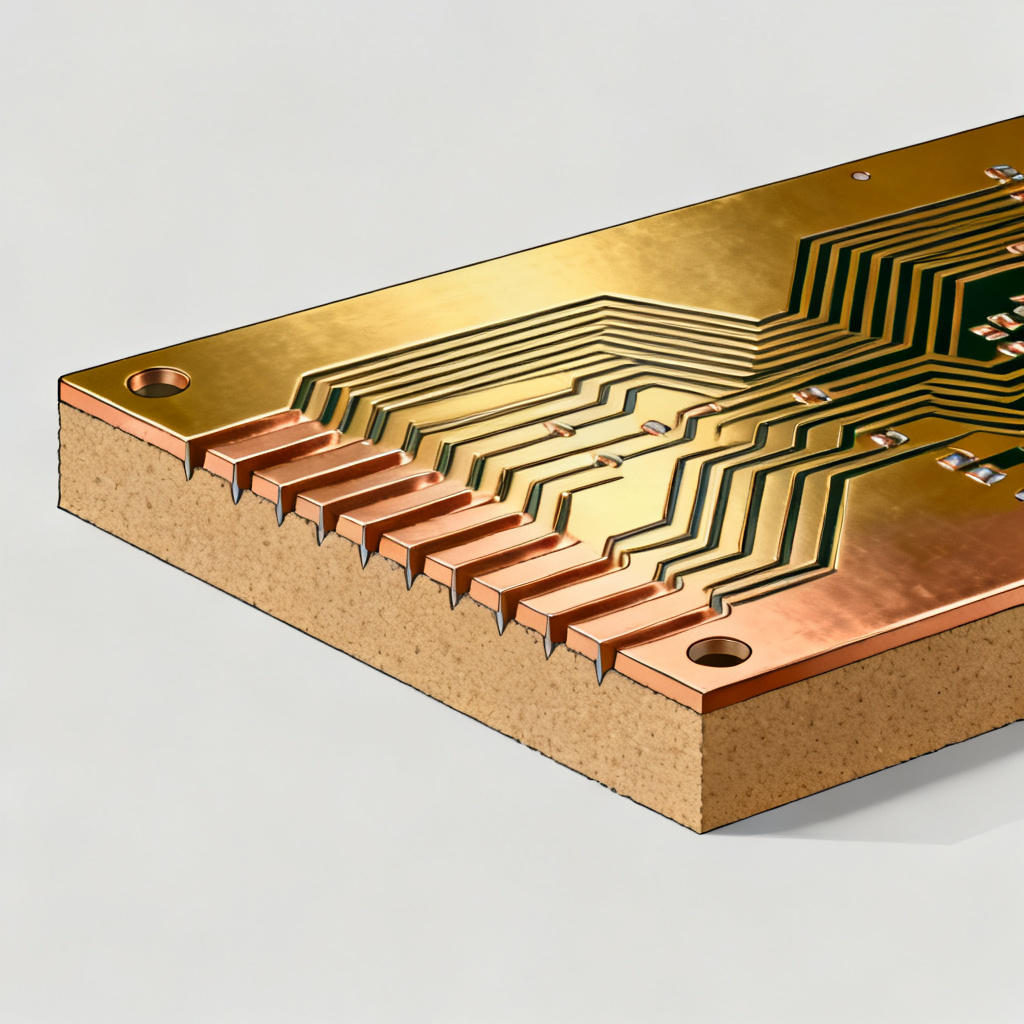
A single-sided rigid PCB has exactly one layer of conductive copper on one side of the substrate. All traces, pads, and components are on this same side.
Advantages of Single-Sided Rigid PCBs
- Lowest Cost: Simple manufacturing, ideal for high-volume, low-complexity products.
- Fast Turnaround: Quickest lead times due to minimal fabrication steps.
- Easy to Design and Repair: Simple layout and straightforward troubleshooting.
Disadvantages of Single-Sided Rigid PCBs
- Limited Complexity: Cannot support dense component placement or complex routing.
- No Cross-Over Traces: Requires jumper wires or zero-ohm resistors for crossing traces.
- Poor Electromagnetic Performance: No ground or power plane, leading to higher EMI.
Common Applications for Single-Sided Rigid PCBs
- Consumer electronics: calculators, coffee makers, LED lighting.
- Industrial: simple sensors, relay drivers, power supplies.
- Automotive: basic dashboard indicators, simple control modules.
Design Considerations for Single-Sided Rigid PCBs
- Trace Width and Spacing: For 1 oz copper, 10 mil trace/space is a safe minimum for low-voltage designs.
- Component Placement: Place all components on the copper side; through-hole components soldered on trace side.
- Drill Sizes: Standard drills from 0.3mm to 1.0mm; avoid micro-vias under 0.2mm.
Cost Factors for Single-Sided Rigid PCBs
- Board Size: Larger boards use more material.
- Copper Weight: 2 oz copper costs more than 1 oz.
- Surface Finish: HASL is cheapest; ENIG adds cost for better flatness and shelf life.
Double-Sided Rigid PCBs – The Industry Standard
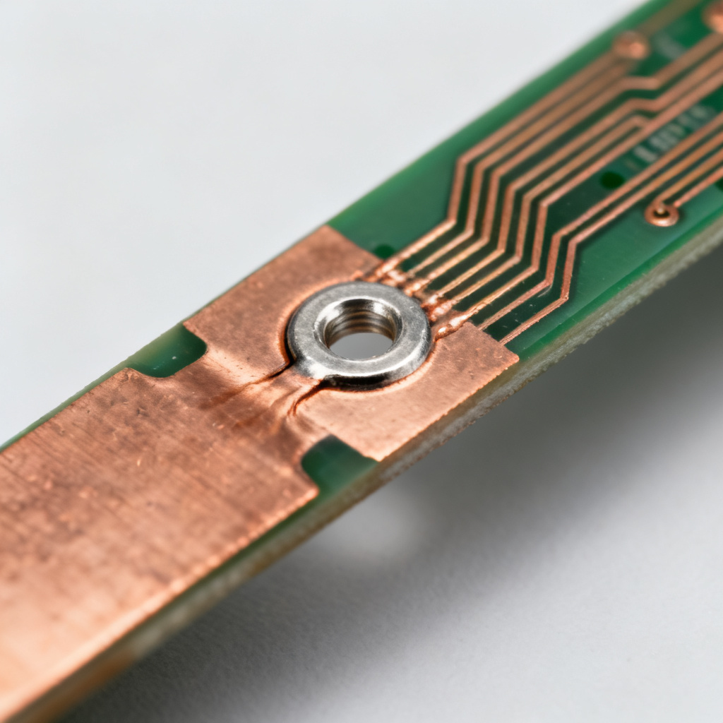
A double-sided rigid PCB has two conductive copper layers connected by plated through-holes (PTH), also known as vias. This enables more complex routing and better signal integrity.
Advantages of Double-Sided Rigid PCBs
- Higher Density: Allows complex routing and component placement on both sides.
- Better Signal Integrity: Can incorporate dedicated ground and power planes.
- Cross-Over Capability: Traces can cross using vias to switch layers.
- Moderate Cost: Slightly more expensive than single-sided but vastly superior performance.
Disadvantages of Double-Sided Rigid PCBs
- More Complex Manufacturing: Requires precise drilling and copper plating of vias.
- Requires Careful Design: Designers must consider impedance control and via placement.
Common Applications for Double-Sided Rigid PCBs
- Industrial controls: PLCs, motor drives, power inverters.
- Consumer electronics: smartphones, laptops, audio amplifiers.
- Automotive: engine control units (ECUs), infotainment systems.
- Telecommunications: Ethernet switches, routers, base stations.
Design Considerations for Double-Sided Rigid PCBs
- Via Types: Through-hole via is most common and cost-effective.
- Impedance Control: For high-speed signals (USB, HDMI, Ethernet), control trace width and distance to ground plane.
- Thermal Management: Use thermal vias under hot components to dissipate heat.
Cost Factors for Double-Sided Rigid PCBs
- Layer Count: Double-sided is baseline for multi-layer pricing.
- Via Count: More vias increase drilling and plating time.
- Minimum Trace/Space: Tighter tolerances increase cost.
- Board Thickness: Standard 1.6mm is cheapest.
Multilayer Rigid PCBs – The High-Performance Powerhouse
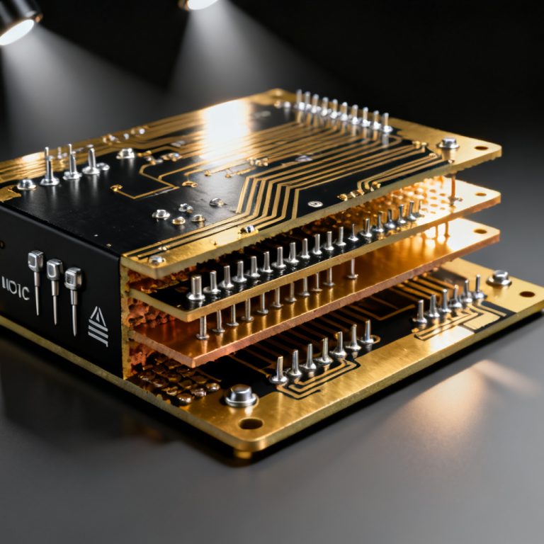
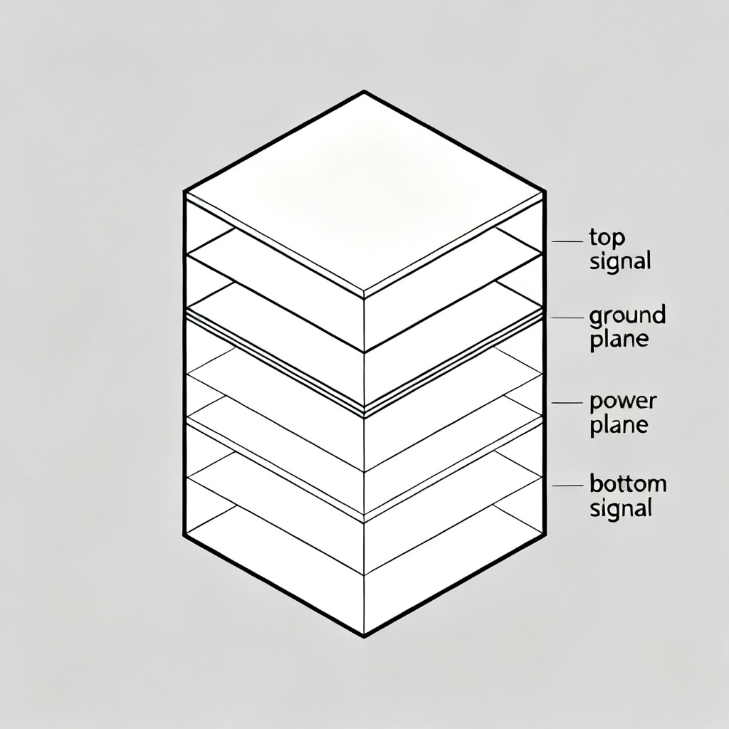
A multilayer rigid PCB consists of three or more conductive copper layers laminated together. Common layer counts are 4, 6, 8, 10, and up to 60+ for advanced applications. A typical 4-layer stackup includes top signal, inner ground, inner power, and bottom signal layers.
Advantages of Multilayer Rigid PCBs
- Extreme Density: Accommodates thousands of components in a small footprint.
- Superior Signal Integrity: Dedicated ground and power planes reduce EMI and crosstalk.
- Excellent Thermal Management: Internal copper planes act as heat spreaders.
- Reduced Size and Weight: Enables miniaturization of electronic devices.
- High Reliability: Robust mechanical structure and vibration resistance.
Disadvantages of Multilayer Rigid PCBs
- Highest Cost: Complex lamination, drilling, and plating processes.
- Longer Lead Times: More layers require more manufacturing steps.
- Difficult to Repair: Internal layers are inaccessible.
- Complex Design: Requires advanced EDA tools and experienced engineers.
Common Applications for Multilayer Rigid PCBs
- High-end computing: servers, GPUs, motherboards.
- Telecommunications: 5G base stations, optical transceivers.
- Medical devices: MRI machines, CT scanners, implantable devices.
- Aerospace and defense: avionics, radar systems, satellite electronics.
- Automotive: ADAS, electric vehicle battery management systems.
Design Considerations for Multilayer Rigid PCBs
- Stackup Planning: Most critical step; define layer order based on signal types and power requirements.
- Impedance Control: Essential for all high-speed signals; work with manufacturer on dielectric constant (Dk) and prepreg thickness.
- Via Technology: Microvia, buried via, via-in-pad, blind and buried vias reduce layer count but increase cost.
- Design for Manufacturing (DFM): Ensure balanced stackup to prevent warpage; avoid copper imbalances.
Cost Factors for Multilayer Rigid PCBs
- Layer Count: Each additional layer adds material and cost; 6-layer is roughly 1.5x cost of 4-layer.
- Board Size: Larger boards with many layers become exponentially more expensive.
- Aspect Ratio: High aspect ratios (>10:1) increase difficulty and cost.
- Material Grade: High-Tg FR-4, low-loss materials (Rogers, PTFE), halogen-free laminates add cost.
- Surface Finish: ENIG is most common for high-reliability multilayer boards.
Comparative Analysis – Single vs. Double vs. Multilayer Rigid PCBs
| Feature | Single-Sided Rigid PCB | Double-Sided Rigid PCB | Multilayer Rigid PCB (4+ Layers) |
|---|---|---|---|
| Layer Count | 1 | 2 | 3+ |
| Circuit Density | Low | Medium | High |
| Signal Integrity | Poor | Good | Excellent |
| EMI Performance | Poor | Moderate | Excellent |
| Thermal Management | Poor | Moderate | Excellent |
| Cost (per board) | Low | Medium | High |
| Lead Time | Short (1-3 days) | Standard (3-7 days) | Long (7-20+ days) |
| Complexity | Simple | Moderate | Complex |
| Repairability | Easy | Moderate | Difficult |
| Typical Applications | Simple consumer goods | Industrial, automotive | High-speed computing, telecom, medical |
How to Choose the Right Rigid PCB for Your Project
A practical decision framework for B2B buyers:
- Start with Circuit Complexity: Count nets; under 50 nets may suit single-sided; 50-200 nets ideal for double-sided; over 200 nets or high-speed signals (>50 MHz) move to multilayer.
- Evaluate Signal Speed: For digital signals above 50 MHz or analog signals requiring high precision, a ground plane is mandatory, ruling out single-sided boards.
- Assess Power Requirements: Multiple voltage rails or high currents (>2A) benefit from multilayer with dedicated power planes.
- Consider Physical Constraints: Compact products require multilayer; if size is not constrained, single or double-sided may be more economical.
- Budget and Volume: High-volume, low-cost products favor single-sided; medium-volume, mid-complexity products suit double-sided; low-volume, high-performance products justify multilayer.
Manufacturing Process Overview (For All Types)
- Design and File Preparation: Gerber files, drill files, stackup documentation.
- Inner Layer Imaging and Etching (Multilayer only): Inner layers are imaged and etched.
- Lamination (Multilayer only): Inner layers stacked with prepreg and copper foil, pressed under heat and pressure.
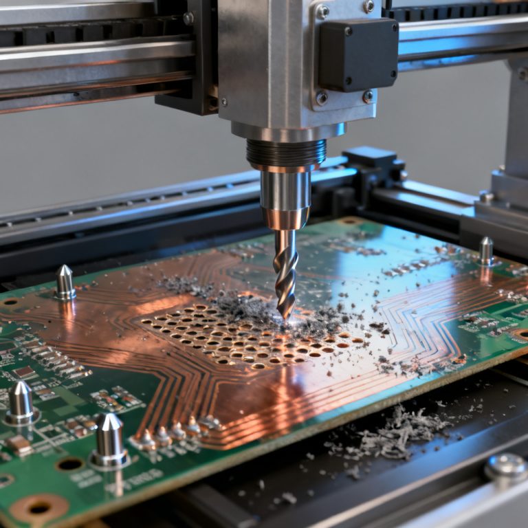
- Drilling: Holes drilled for PTH or partially for blind/buried vias.
- Plating: Thin copper deposited on hole walls for electrical connections.
- Outer Layer Imaging and Etching: Top and bottom copper layers imaged and etched.
- Solder Mask Application: Protective solder mask applied and cured.
- Surface Finish: Copper pads coated with finish (HASL, ENIG, OSP, etc.).
- Silkscreen: Legend printed.
- Electrical Testing: Continuity and isolation testing.
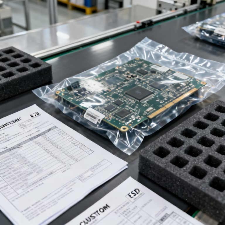
- Final Inspection and Packaging: Visual inspection, panelization, packaging.
Common Pitfalls and DFM Tips for B2B Buyers
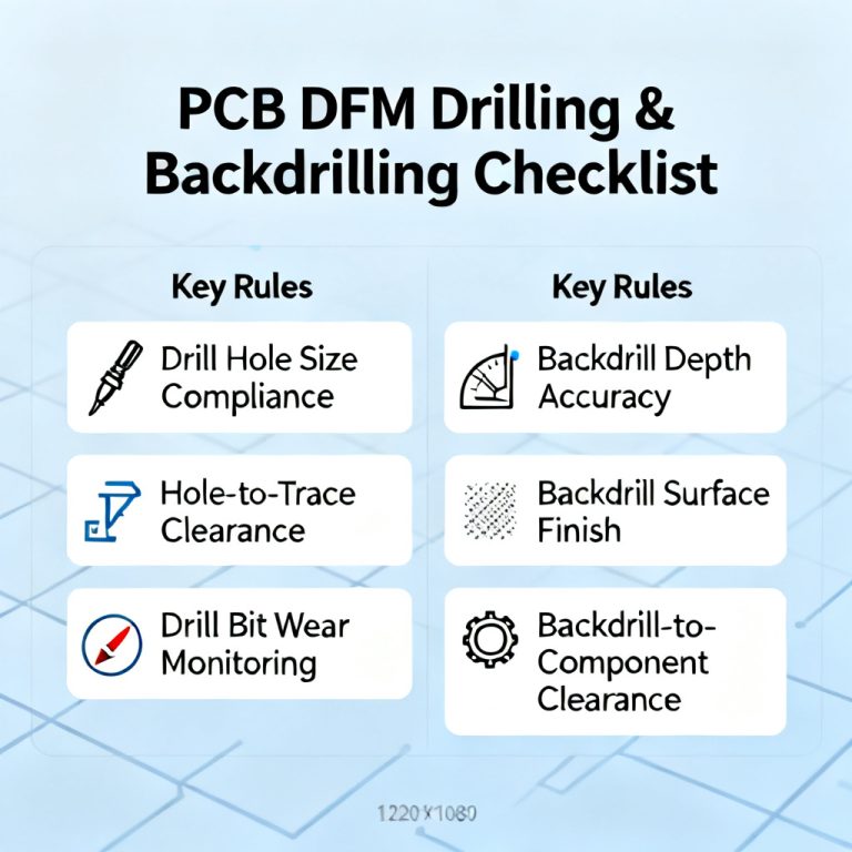
- Ignoring DFM Rules: Copper imbalance causes warpage; insufficient annular ring weakens connections; acid traps from sharp angles.
- Underestimating Lead Times: Multilayer boards with blind/buried vias or exotic materials require longer lead times.
- Not Specifying Material Grade: Standard FR-4 unsuitable for high-temperature or high-frequency environments; specify High-Tg FR-4 or low-loss materials.
- Over-Specifying Tolerances: Tight tolerances increase cost without real benefit; use standard tolerances unless necessary.
Frequently Asked Questions About Rigid PCBs
What is the difference between single-sided and double-sided rigid PCBs?
Single-sided rigid PCBs have one copper layer, while double-sided rigid PCBs have two layers connected by plated through-holes, enabling more complex routing and better signal integrity.
When should I choose a multilayer rigid PCB?
Choose a multilayer rigid PCB when you need high circuit density, superior signal integrity for high-speed signals, excellent thermal management, or compact product design with over 200 nets.
What is the typical lead time for a rigid PCB?
Single-sided rigid PCBs can ship in 1-3 days, double-sided in 3-7 days, and multilayer rigid PCBs typically require 7-20+ days depending on layer count and complexity.
How does copper weight affect rigid PCB performance?
Standard copper weight is 1 oz/ft² (35µm). For high-current designs, 2 oz (70µm) is common. Heavier copper increases current capacity and thermal dissipation but also increases cost.
What is Tg in rigid PCB materials?
Tg (glass transition temperature) is the temperature at which the substrate begins to soften. Standard FR-4 has a Tg of 130-140°C; High-Tg FR-4 (170-180°C) is used for lead-free soldering and high-reliability applications.
Why Choose Us for Your Rigid PCB Needs
We are your trusted B2B partner for all rigid PCB requirements, from prototype to high-volume production. We offer free DFM review, competitive pricing on all layer counts and materials, fast lead times (as quick as 24 hours for single-sided prototypes), and expert engineering support to help you choose the right stackup and materials. Request a quote today for your next rigid PCB project.