Impedance Parameters Target Tolerance and Coupon
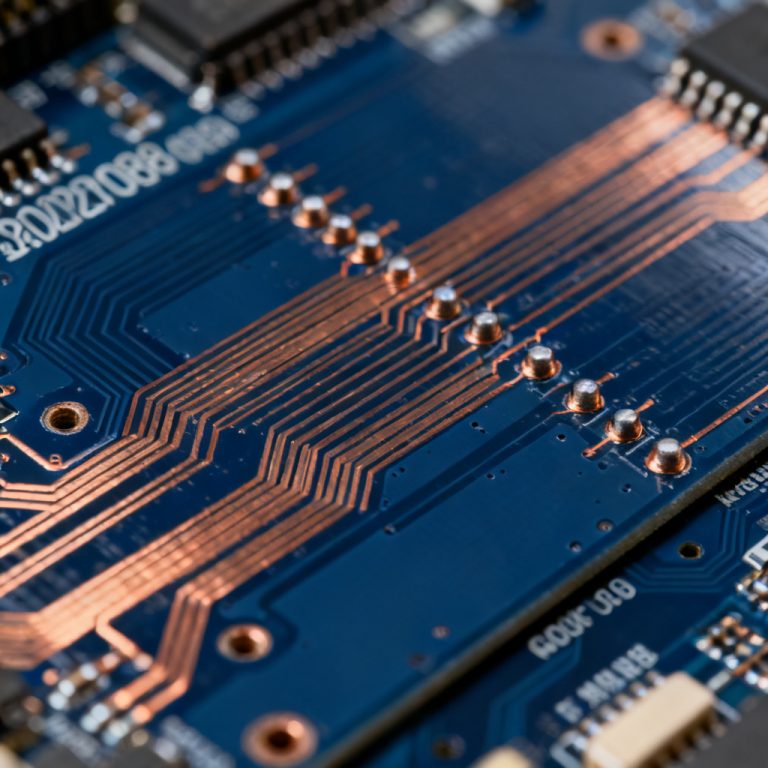
In high-speed digital and RF PCB design, controlled Impedance Parameters Target Tolerance and Coupon—are fundamental for signal integrity. As a B2B PCB manufacturer, we ensure your design meets these critical specifications.
Target Impedance: The Design Specification
The impedance parameters start with the target impedance, the desired characteristic impedance for your transmission line. This is determined by your IC vendor’s datasheet or high-speed interface standard.

Common Target Values
- Single-ended: 50 Ω (most common for RF, general high-speed digital)
- Differential: 90 Ω (USB 2.0/3.0, HDMI), 100 Ω (LVDS, Ethernet, PCIe), 85 Ω (some DDR4/DDR5)
- Other: 75 Ω (video/coaxial), 28 Ω (some high-power RF)
Factors That Determine the Target
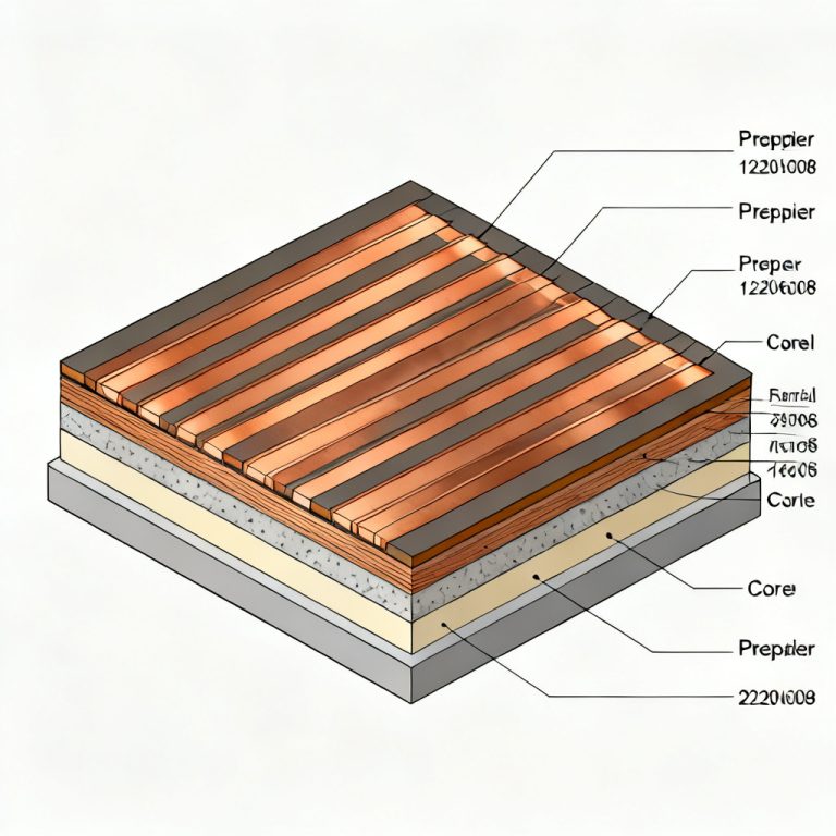
The target impedance is a function of physical geometry and material properties: trace width (W), trace thickness (T), dielectric height (H), dielectric constant (Dk or εr), and copper roughness. A field solver (like Polar Si8000) is recommended for accurate calculation.
| Impedance Parameter | Description | Impact on Target |
|---|---|---|
| Trace Width (W) | Width of the copper trace | Wider traces lower impedance |
| Dielectric Height (H) | Distance to reference plane | Larger height increases impedance |
| Dielectric Constant (Dk) | Material permittivity | Higher Dk lowers impedance |
Impedance Tolerance: The Manufacturing Reality
Impedance parameters include tolerance, which defines the acceptable deviation from the target. No manufacturing process is perfect, so specifying realistic tolerances is crucial.

Standard Industry Tolerances
- ±10%: Standard, economical for most high-speed digital designs (e.g., 50 Ω ± 5 Ω)
- ±7%: Tight tolerance for high-performance boards or advanced materials
- ±5%: Very tight tolerance for military, aerospace, or high-speed memory interfaces
- <±5%: Extremely tight, achievable only with exotic materials and specialized processes
What Affects Tolerance?
Material variation (FR4 Dk can vary by ±5-10%), etching variation, lamination pressure, and copper thickness variation all impact tolerance. Over-specifying tolerance increases cost unnecessarily.
Impedance Coupon: The Verification Tool
The impedance parameters are verified using an impedance coupon, a small test structure attached to the production panel. This is the only reliable way to confirm the fabricated board meets target and tolerance.

Why Use a Coupon?
- Non-destructive: You cannot measure impedance on the actual board without destroying it
- Process Validation: Confirms the entire manufacturing process produced correct geometry
- Batch Consistency: Allows for statistical process control across panels and runs
Coupon Design Requirements
Based on IPC-2141, a properly designed coupon must have the same layer stackup, trace geometry, reference planes, and be long enough for TDR measurement (minimum 3 inches).
| Coupon Element | Requirement | Purpose |
|---|---|---|
| Layer Structure | Same as production board | Accurate process replication |
| Trace Geometry | Identical width, spacing, length | Representative measurement |
| Reference Planes | Solid copper planes | Consistent impedance environment |
Measurement Method: TDR
Impedance is measured using Time Domain Reflectometry (TDR). A fast rise-time pulse is sent down the trace, and the reflected energy is measured to calculate impedance.
How to Specify Impedance on Your Fabrication Drawing
To ensure your board is built correctly, include an explicit impedance parameters table on your fabrication drawing.
| Net Class | Target (Ω) | Tolerance | Layer | Trace Type |
|---|---|---|---|---|
| USB_DP/DM | 90 (Diff) | ±10% | Top | Microstrip |
| DDR_DQ | 50 (SE) | ±7% | L3 | Stripline |
| RF_Antenna | 50 (SE) | ±5% | Top | Coplanar WG |
Common Pitfalls and Best Practices
Pitfall 1: Ignoring Material Dk Variation
Solution: Use a material with a specified Dk tolerance (e.g., FR4 with Dk = 4.2 ± 0.15). For tight tolerances, use high-performance laminates like Rogers.
Pitfall 2: Using Inaccurate Stackup Data
Solution: Provide your fabricator with the exact stackup they will use. Many fabricators offer stackup optimization services.
Pitfall 3: Designing a Coupon That Doesn’t Match the Board
Solution: The coupon must be a faithful replica of the production board, including all unique layer and impedance values.
Pitfall 4: Specifying Unnecessary Tight Tolerances
Solution: A 50 Ω ± 5% trace is much harder and more expensive than ±10%. Only specify tight tolerances where required.
Pitfall 5: Forgetting About Solder Mask
Solution: Solder mask lowers outer layer impedance by 2-5 Ω. Include its thickness in calculations.
Conclusion: Partnering for Success
Controlled impedance parameters are a collaborative effort between designer and manufacturer. By clearly specifying target, tolerance, and coupon requirements, you empower your PCB fabricator to deliver boards meeting your signal integrity needs.
At [Your Company Name], we specialize in high-reliability PCBs with precise impedance control, offering free stackup analysis, tight tolerance capabilities down to ±5%, custom coupon design, and full TDR testing with detailed reports.
Frequently Asked Questions about Impedance Parameters
What is the difference between target impedance and tolerance?
Target impedance is the desired value (e.g., 50 Ω), while tolerance defines the acceptable deviation (e.g., ±10%). Both are critical impedance parameters for signal integrity.
Why is an impedance coupon necessary?
An impedance coupon allows non-destructive verification that the fabricated board meets the specified impedance parameters using TDR measurement.
How tight can impedance tolerance be?
Standard tolerance is ±10%, while tight tolerance is ±7% or ±5%. Extremely tight tolerances (<±5%) require exotic materials and specialized processes.
What factors affect impedance tolerance during manufacturing?
Material Dk variation, etching variation, lamination pressure, and copper thickness variation all impact impedance parameters tolerance.
How do I specify impedance parameters on my fabrication drawing?
Include an explicit impedance table with net class, target, tolerance, layer, and trace type. Also provide a detailed stackup drawing and coupon requirements.