LED PCB Guide Aluminum Backed Thermal Conductivity Layout
This comprehensive LED PCB Guide Aluminum Backed Thermal Conductivity Layout manual delivers advanced metal core board design rules for hardware engineers. Light Emitting Diodes (LEDs) have revolutionized commercial lighting, but their performance and lifespan are intrinsically tied to thermal management. Since standard FR-4 substrates are poor thermal conductors, utilizing specialized aluminum-backed configurations is critical to prevent lumen depreciation and premature component failure.
Introduction: Why LED PCBs Demand Specialized Design
An LED PCB is a specialized circuit board designed to mount and cool high-power LEDs. Unlike standard PCBs, an LED PCB must handle both electrical current and significant thermal load. This guide is the ultimate resource for engineers, procurement managers, and electronics designers. We will dissect the three pillars of successful LED PCB design: the aluminum-backed structure, the science of thermal conductivity, and the art of layout optimization. By the end, you will understand how to specify, design, and source the perfect PCB for your LED application, from simple indicators to high-lumen architectural lighting.
Part 1: The Aluminum Backed PCB (Metal Core PCB – MCPCB)
1.1 What is an Aluminum Backed PCB?
An aluminum-backed PCB, more formally known as a Metal Core PCB (MCPCB), is a type of PCB that uses a metal base material (typically aluminum, but sometimes copper for extreme heat) as the core instead of the standard epoxy-glass (FR-4). Its primary purpose is to provide superior heat dissipation and mechanical stability for high-power components, especially LEDs.
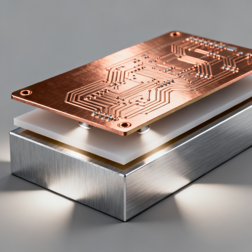
1.2 The Layer Structure of an Aluminum PCB
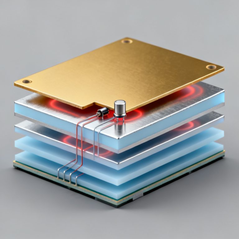
A standard aluminum-backed PCB is a three-layer sandwich:
- Copper Circuit Layer (Top Layer): This is the standard copper foil (1 oz to 4 oz or more) etched to form the electrical circuit. Thicker copper (e.g., 2 oz or 3 oz) is often recommended for high-current LED applications to reduce resistive losses and improve heat spreading.
- Thermally Conductive Dielectric Layer (The Key): This is the most critical layer. It is a specialized polymer or epoxy material filled with ceramic particles (e.g., aluminum oxide, boron nitride). Its function is to electrically insulate the copper circuit from the metal core while simultaneously conducting heat from the copper layer to the aluminum base. The thermal conductivity of this dielectric (measured in W/mK) is the primary performance differentiator. Common values range from 0.8 W/mK for standard materials to 3.0 W/mK or higher for high-performance dielectrics.
- Aluminum Base Layer (Core): This is the thick, structural base (typically 0.8mm to 3.2mm thick). It provides mechanical rigidity and acts as a massive heat sink, spreading heat from the small LED footprint to a larger area for convection cooling. Common alloys include 1050, 5052, and 6061, with 1050 offering the highest thermal conductivity.
1.3 Advantages of Aluminum Backed PCBs for LEDs
- Superior Heat Dissipation: The primary benefit. Thermal resistance is dramatically lower than FR-4, keeping LED junction temperatures within safe limits.
- Increased Lifespan: By reducing thermal stress, LEDs can operate for their rated 50,000 to 100,000+ hours.
- Higher Lumen Output: Cooler LEDs operate more efficiently, producing more light per watt.
- Mechanical Strength: The aluminum core provides excellent rigidity, making the board resistant to vibration and shock.
- EMI Shielding: The aluminum layer can act as a natural shield against electromagnetic interference, though it is not always grounded.
- Light Weight & Thin Profile: Aluminum is lighter and can be made thinner than a comparable FR-4 board with an external heatsink.
1.4 Limitations and Considerations
- Cost: MCPCBs are more expensive than standard FR-4 PCBs due to the specialized materials and manufacturing process.
- Single-Sided Designs: Most aluminum PCBs are single-sided because drilling through the metal core and plating vias is complex and costly. Double-sided MCPCBs are possible but less common.
- Thermal Expansion (CTE Mismatch): The Coefficient of Thermal Expansion (CTE) of aluminum (approx. 23 ppm/°C) differs significantly from copper (17 ppm/°C) and ceramic components (6-8 ppm/°C). This mismatch can cause stress on solder joints during thermal cycling. High-quality dielectrics are designed to buffer this stress.
- Not for High-Frequency Circuits: The dielectric layer and metal core can create parasitic capacitance, making them unsuitable for RF circuits operating above a few GHz.
Part 2: Thermal Conductivity – The Core Science
2.1 Why Thermal Management is Non-Negotiable
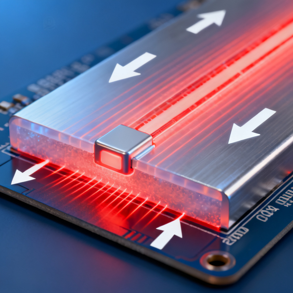
An LED’s junction temperature (Tj) is the single most important factor determining its performance and reliability. For every 10°C increase in Tj above the rated maximum (e.g., 85°C or 125°C), the lifespan can be halved. The goal of thermal management is to minimize the thermal resistance (Rth) from the LED junction to the ambient air. The path is:
Junction → LED Substrate → Solder → PCB Copper Pad → Dielectric Layer → Aluminum Core → (Optional) External Heatsink → Ambient Air
2.2 Key Thermal Parameters & Calculations
- Thermal Conductivity (k): Measured in Watts per meter-Kelvin (W/mK). This is the material’s intrinsic ability to conduct heat. Higher is better. Copper is ~400 W/mK, Aluminum is ~200 W/mK, a good dielectric is 1-3 W/mK, and FR-4 is a poor 0.3 W/mK. The dielectric layer is the bottleneck.
- Thermal Resistance (Rth): Measured in °C/W. This quantifies the temperature rise per watt of power dissipated. Total Rth is the sum of all resistances in the path. The goal is to minimize total Rth.
- Calculating Required PCB Performance:
- Determine LED Power (P): Forward Voltage (Vf) x Forward Current (If) – (Optical Power). For a rough estimate, use electrical power.
- Find Max Junction Temp (Tj_max): From the LED datasheet (e.g., 85°C or 125°C).
- Determine Ambient Temp (Ta): The operating environment (e.g., 25°C indoors, 50°C in a fixture).
- Calculate Allowable Temperature Rise: ΔT = Tj_max – Ta.
- Calculate Maximum Total Thermal Resistance: Rth_total_max = ΔT / P.
- Select PCB/Heatsink: The sum of the LED’s internal Rth (Rth_js), the solder joint Rth, the PCB’s Rth, and any heatsink’s Rth must be less than Rth_total_max.
2.3 Optimizing Thermal Performance in the Dielectric Layer
- Dielectric Thickness: A thinner dielectric layer reduces thermal resistance but increases the risk of electrical breakdown (voltage isolation). Standard thicknesses are 50µm, 75µm, and 100µm. For high-voltage LED drivers (e.g., > 100V), a thicker dielectric (e.g., 100-150µm) is required for safety, which increases thermal resistance. A trade-off exists.
- Filler Material: The type of ceramic filler (alumina, BN, AlN) and its loading percentage within the polymer matrix determine the dielectric’s thermal conductivity. Higher filler loading improves k but can make the material more brittle.
- Thermal Vias (in FR-4 or Hybrid Boards): While less common in pure MCPCBs, some designs use a standard FR-4 board with an array of plated through-holes (thermal vias) filled with conductive epoxy or solder to transfer heat to a metal core or heatsink on the bottom. This is a cost-effective alternative for lower-power LEDs.
2.4 Measuring Thermal Performance
- Thermal Resistance Test: Using a thermal test vehicle (e.g., a standard JEDEC board), the Rth of the PCB can be measured by applying a known power and measuring the temperature rise using a thermocouple or IR camera.
- Standardized Values: Look for PCB datasheets that specify Rth (°C/W) for a given copper pad size and dielectric thickness. This allows direct comparison between different MCPCB suppliers.
Part 3: PCB Layout Design for LEDs – Practical Rules
3.1 Copper Pad and Trace Design for Heat Spreading
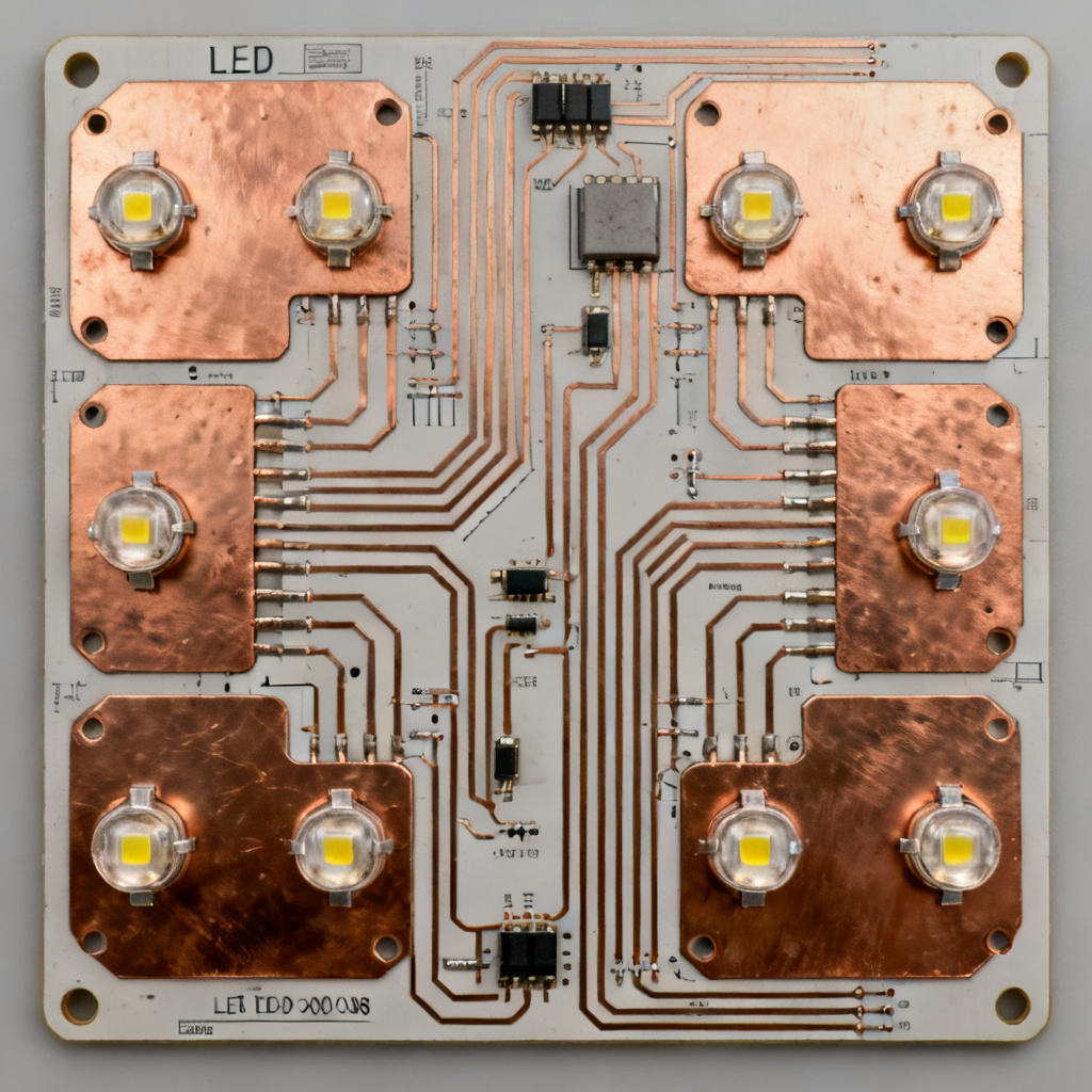
- Maximize Copper Coverage: On the top layer, use as much copper as possible around the LED’s thermal pad. Do not use a “via-in-pad” design unless absolutely necessary, as it can create solder voids. Instead, use wide, solid copper pours.
- Thermal Pad Size: The LED’s exposed thermal pad (often on the bottom of the component) must be soldered directly to a matching copper pad on the PCB. This pad should be slightly larger than the component’s pad to allow for solder fillet formation. For multi-die LEDs, ensure the pad is continuous.
- Trace Width for Current: For high-current LEDs (e.g., 1A or more), trace width is critical. Use a PCB trace width calculator to determine the required width to keep temperature rise below 10°C. For example, a 1 oz copper trace carrying 3A needs to be approximately 120 mils (3mm) wide. Use 2 oz or 3 oz copper for high-current paths to reduce trace width and resistive losses.
- Avoid Acute Angles: Route traces with 45-degree angles or arcs, not 90-degree corners, to avoid acid traps and reduce impedance discontinuities.
3.2 Component Placement & Thermal Isolation
- LED Spacing: Do not place LEDs too close together. The heat from one LED will heat its neighbor, raising the local temperature. Follow the LED manufacturer’s recommended spacing, typically based on the board’s thermal performance.
- Heat-Sensitive Components: Place temperature-sensitive components (e.g., electrolytic capacitors, voltage regulators, sensors) as far away from the LED cluster as possible. Capacitor lifespan is heavily dependent on operating temperature.
- Driver Circuit Isolation: If the LED driver is on the same PCB, place it on a separate copper island or at the edge of the board to prevent its heat from adding to the LED’s thermal load.
3.3 Grounding and Electrical Design
- Star Grounding: For multiple LED strings, use a star-ground topology. Each LED’s cathode should have a dedicated trace back to a single point on the ground plane (or the aluminum core if it is used as a ground). This prevents ground loops and current imbalances.
- Copper Pour for Ground: Use a large copper pour on the top layer for the ground connection, connected to the cathode pads. This provides a low-impedance return path and aids heat spreading.
- Aluminum Core Grounding: The aluminum core can be left electrically floating or connected to ground. If grounded, it can act as an EMI shield. However, ensure the dielectric layer provides sufficient isolation (e.g., 1500VAC) between the circuit and the core. A common practice is to connect the core to ground through a high-voltage capacitor (e.g., 1nF, 2kV) to provide an RF ground path while blocking DC.
- ESD Protection: Place TVS diodes or Zener diodes near the LED input terminals to protect against electrostatic discharge (ESD), which can instantly damage LEDs.
3.4 Solder Mask and Silkscreen
- Solder Mask: Use a standard green solder mask over the copper traces. For the LED’s thermal pad, use a solder mask defined (SMD) pad to prevent solder from wicking away from the pad. Alternatively, use a non-solder mask defined (NSMD) pad with a small solder mask opening slightly smaller than the pad to create a “dam” that controls solder flow.
- Silkscreen: Clearly label all test points, LED strings (e.g., “LED String 1”), and polarity (+/-). Include a unique PCB revision number and date.
3.5 Advanced Layout Techniques
- Copper Coin Technology: For extreme heat dissipation (e.g., > 50W), a copper coin or slug can be embedded into the aluminum core. This provides a direct, low-resistance thermal path from the LED to the bottom of the board.
- Insulated Metal Substrate (IMS): This is another term for an MCPCB. It is the same three-layer structure.
- Hybrid Boards: Combining FR-4 for driver circuitry and MCPCB for the LED array on a single panel. This is a cost-effective solution for complex designs.
Part 4: Manufacturing & Sourcing Considerations

4.1 Key Specifications for Your PCB Manufacturer
When ordering your LED PCB, provide these critical parameters to ensure quality:
- Material Stack-up: Specify the exact layer structure: Copper thickness (e.g., 2 oz), Dielectric type and thickness (e.g., 75µm, 1.5 W/mK), and Aluminum core thickness (e.g., 1.6mm, alloy 1050).
- Thermal Performance Data: Request the Rth value for your specific pad size and dielectric. Ask for a thermal test report if available.
- Tolerance: Specify tight tolerances for hole positions and pad dimensions, especially for high-density LED arrays.
- Surface Finish: ENIG (Electroless Nickel Immersion Gold) is the preferred finish for LED PCBs because it provides a flat, solderable surface and excellent corrosion resistance. HASL (Hot Air Solder Leveling) is cheaper but can create uneven surfaces unsuitable for fine-pitch LEDs. OSP (Organic Solderability Preservative) is a low-cost option but has a shorter shelf life.
- Voltage Withstand (Hi-Pot Test): Specify the required dielectric strength (e.g., 1500VAC or 3000VDC) between the circuit and the aluminum core. The manufacturer should perform a hi-pot test on every panel.
- Solder Mask Type: Specify a high-temperature solder mask (e.g., LPI) that can withstand reflow soldering temperatures (260°C).
- Certifications: Request UL 796 (for PCB) certification for the finished board, especially if it will be used in a UL-listed luminaire.
4.2 Common Pitfalls to Avoid
- Underestimating Thermal Resistance: Using a cheap MCPCB with a low-k dielectric (e.g., 0.8 W/mK) for a high-power LED (e.g., 10W) will result in early failure.
- Ignoring CTE Mismatch: Using a very thick aluminum core (e.g., 3mm) with a brittle dielectric can lead to delamination after repeated thermal cycling.
- Poor Layout: Using thin traces for high current will cause voltage drop and localized heating.
- Incorrect Solder Paste: Using standard lead-free solder paste may not be suitable for high-temperature LED applications. Use a high-reliability, high-temperature solder paste.
- Failing to Specify Voltage Isolation: For commercial and industrial lighting, safety regulations require high voltage isolation (e.g., 1500VAC) between the circuit and the metal core. Always specify this.
Conclusion: The Path to a Successful LED PCB
Designing a reliable LED PCB is a multi-disciplinary challenge that demands a deep understanding of thermal physics, electrical engineering, and materials science. The three pillars—Aluminum Backed Structure, Thermal Conductivity, and Layout—are inseparable. A failure in any one will compromise the entire system.
By choosing the correct MCPCB material, calculating your thermal budget, and meticulously designing your layout for heat spreading and electrical integrity, you can create LED products that deliver exceptional performance, long life, and high reliability.
Your Next Step: Partner with a PCB manufacturer who understands these nuances. When you are ready to turn your design into a reality, Contact Us for a free DFM (Design for Manufacturability) review and a competitive quote on your aluminum-backed LED PCBs. We specialize in high-thermal-performance boards with fast turnaround times and full UL certification.
Frequently Asked Questions (FAQ) about LED PCBs
What is the difference between an LED PCB and a standard PCB?
How do I calculate thermal conductivity for my LED PCB?
Can I use an aluminum-backed LED PCB for high-frequency circuits?
What surface finish is best for an LED PCB?
What does MCPCB stand for?
Comparison: Aluminum Backed PCB vs. Standard FR-4 PCB for LED Applications
| Feature | Aluminum Backed PCB (MCPCB) | Standard FR-4 PCB |
|---|---|---|
| Thermal Conductivity | High (1-3 W/mK for dielectric, ~200 W/mK for core) | Low (~0.3 W/mK) |
| Heat Dissipation | Excellent, via metal core | Poor, requires external heatsink |
| LED Lifespan | Extended (50,000-100,000+ hours) | Reduced due to thermal stress |
| Mechanical Strength | High, rigid aluminum core | Lower, more flexible |
| Cost | Higher | Lower |
| Typical Application | High-power LEDs, automotive, industrial lighting | Low-power indicators, consumer electronics |
Glossary of Key LED PCB Terms
- LED PCB: A printed circuit board specifically designed for mounting and cooling LEDs.
- Aluminum Backed PCB: A type of MCPCB using an aluminum core for thermal management.
- Thermal Conductivity (k): A material’s ability to conduct heat, measured in W/mK.
- Thermal Resistance (Rth): The temperature rise per watt of power dissipated, measured in °C/W.
- Dielectric Layer: The insulating layer in an MCPCB that conducts heat but blocks electricity.
- MCPCB: Metal Core Printed Circuit Board.
- CTE: Coefficient of Thermal Expansion, a measure of how much a material expands with temperature.
- ENIG: Electroless Nickel Immersion Gold, a surface finish.
- Hi-Pot Test: High Potential test to verify voltage isolation.