IC Substrate Guide Types Materials Design for Advanced Packaging
This comprehensive IC Substrate Guide Types Materials Design for Advanced Packaging manual covers everything from organic BT and ABF substrates to advanced silicon interposers for hardware engineers. Whether you need a BT substrate for memory modules or an ABF substrate for AI processors, understanding these chip packaging fundamentals is critical for B2B PCB procurement and engineering success.
What is an IC Substrate? Core Functions and Architecture
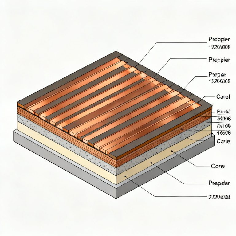
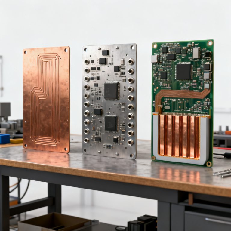
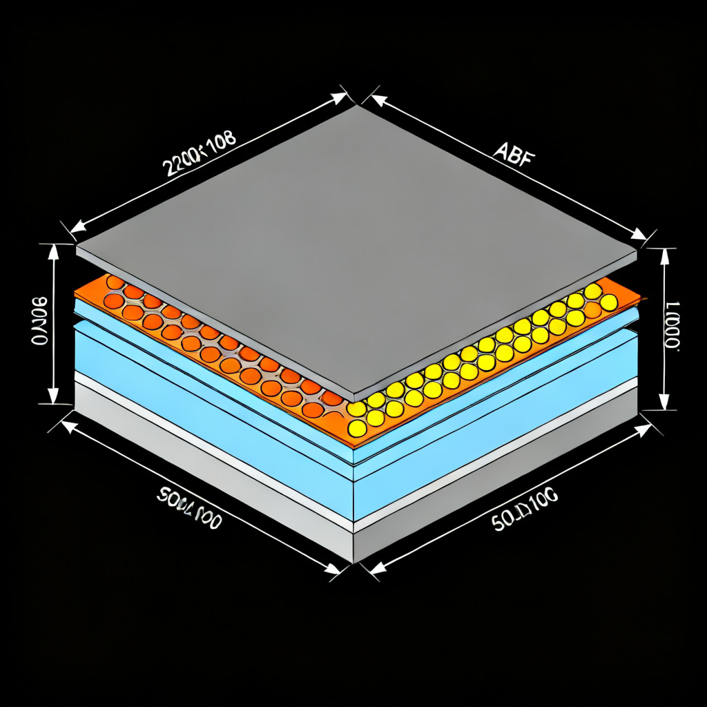
An IC substrate is a specialized printed circuit board that acts as a critical interconnect layer between a semiconductor die and the next level of packaging. Its primary functions include signal distribution, power delivery, thermal management, and mechanical support. A typical IC substrate consists of a core layer (BT resin or glass-reinforced epoxy), build-up layers (ABF film), solder mask, surface finish, and vias (microvias, through-holes, buried vias).
Types of IC Substrates – A Detailed Taxonomy
2.1. Organic IC Substrates (BT & ABF)
Organic substrates are the most common, using resin-based materials. BT (Bismaleimide Triazine) substrates offer excellent dimensional stability and moderate thermal conductivity, ideal for memory modules and logic ICs. ABF (Ajinomoto Build-up Film) substrates enable ultra-fine line/space (down to 8–12µm) and are the dominant choice for high-end CPUs, GPUs, and AI accelerators.
2.2. Ceramic IC Substrates
Ceramic substrates (Alumina, Aluminum Nitride, Beryllium Oxide) are used for high-power and high-reliability applications. They offer extremely high thermal conductivity (AlN: 140–180 W/mK) and excellent electrical insulation, making them ideal for power modules, LED arrays, and automotive electronics.
2.3. Silicon Interposers (2.5D/3D Packaging)
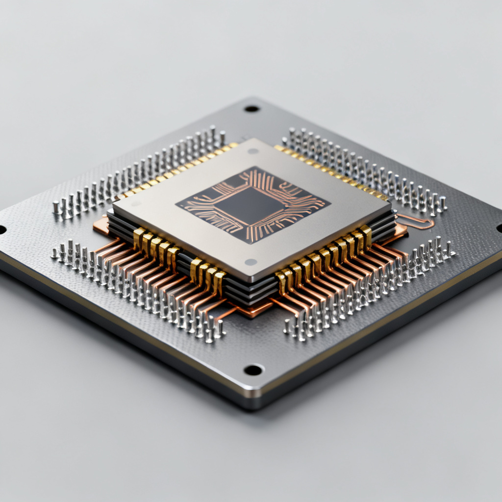
Silicon interposers use high-resistivity silicon wafers with TSVs (Through-Silicon Vias) for vertical connections. They enable the highest density of interconnects and perfect CTE matching with the die, essential for heterogeneous integration (e.g., HBM memory with GPU).
Materials Deep Dive – Choosing the Right Substrate Material
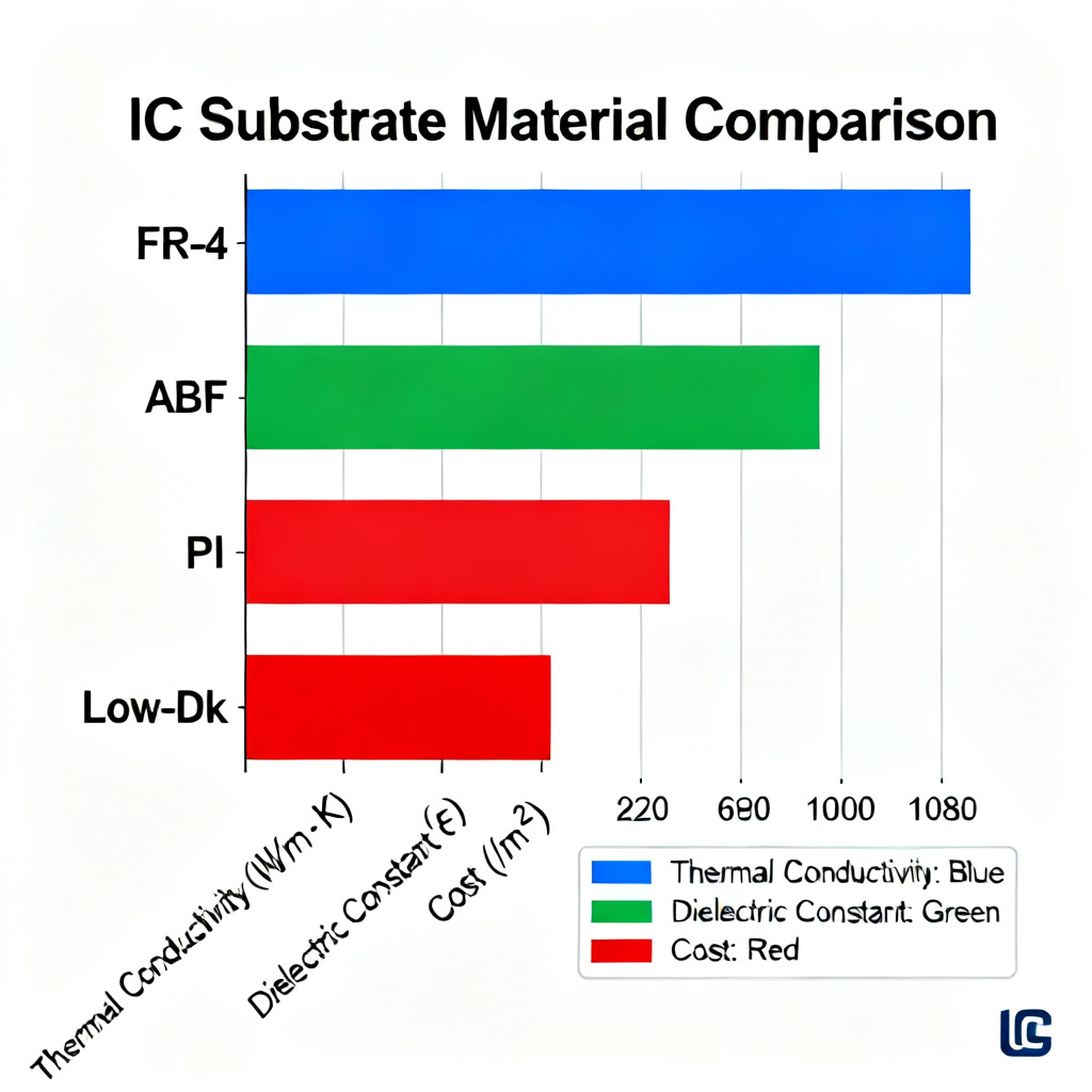
Selecting the correct material is vital for signal integrity, thermal management, and reliability. The table below compares key properties of common IC substrate materials.
| Property | BT Resin | ABF | Alumina (Al₂O₃) | Aluminum Nitride (AlN) | Silicon Interposer |
|---|---|---|---|---|---|
| Dielectric Constant (Dk) | ~4.5–5.0 | ~3.3–3.6 | ~9.8 | ~8.5 | ~11.7 |
| Dissipation Factor (Df) | ~0.015–0.020 | ~0.01–0.02 | ~0.0004 | ~0.0002 | ~0.001 |
| Thermal Conductivity | 0.3–0.5 W/mK | 0.3–0.5 W/mK | 20–30 W/mK | 140–180 W/mK | ~150 W/mK |
| CTE (ppm/°C) | 13–15 | 15–20 | 6–8 | 4.5–5.5 | 2.6 |
| Fine Line Capability | ≥30µm | 8–12µm | ≥100µm | ≥100µm | <1µm |
| Cost | Low | Medium | Medium-High | High | Very High |
| Primary Use | Memory, Logic | CPU, GPU, AI | Power, LED | High-Power | 2.5D/3D HPC |
Key material selection criteria include signal integrity (low Dk/Df materials like ABF), thermal management (AlN or silicon interposers for high-power dies), CTE matching, and reliability (ceramic substrates excel in harsh environments).
Design Rules & Considerations for Advanced Packaging
4.1. Layer Stack-up Design
Core-based substrates (BT) are standard, while coreless substrates allow finer L/S but are thinner. Maintain symmetrical stack-up to prevent warpage. Dedicated power/ground planes are essential for low impedance and noise reduction.
4.2. Trace & Spacing Rules
Minimum L/S for ABF is typically 12/12µm (advanced nodes: 8/8µm), for BT 30/30µm, and for ceramic >100/100µm. Design traces for target impedance (e.g., 50Ω single-ended, 100Ω differential) using microstrip or stripline geometries. Use microvias (laser-drilled, ~50-100µm pad diameter) and avoid stacked microvias without filling.
4.3. Solder Ball & Pad Design
Standard BGA pitch is 0.8mm–1.0mm. Fine-pitch (≤0.5mm) requires advanced assembly. Non-solder mask defined (NSMD) pads are preferred for better solder joint reliability.
4.4. Thermal Management Design
Use arrays of small thermal vias (filled with copper or thermally conductive epoxy) under the die to conduct heat. Some substrates integrate a copper slug or graphite sheet within the core. Use thick copper (2–3oz) on outer layers for heat spreading.
4.5. Signal Integrity & Power Integrity
Ensure continuous ground reference planes to minimize loop inductance. Place decoupling capacitors close to the die on the bottom side of the substrate. Route differential pairs symmetrically with controlled spacing and length matching.
Manufacturing Process – From Design to Finished Substrate
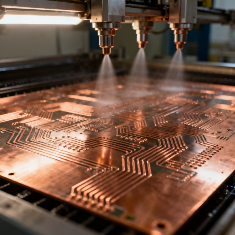
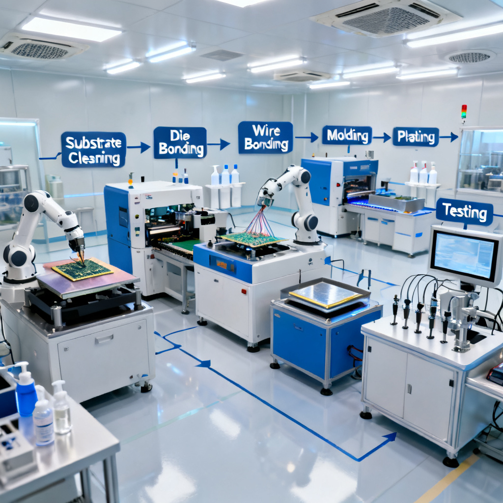
Understanding the manufacturing steps is crucial for design for manufacturability (DFM). The process includes core preparation, lamination of build-up layers, laser drilling, desmear and electroless copper plating, electrolytic copper plating, pattern etching, solder mask application, surface finish (ENIG, ENEPIG, or OSP), electrical testing, and singulation with AOI/X-ray inspection.
Quality & Reliability Testing
For B2B procurement, quality assurance is non-negotiable. Tests include visual & AOI, X-ray inspection, thermal cycling (-55°C to +125°C), moisture sensitivity level (MSL) testing, high-temperature operating life (HTOL), and impedance TDR.
Future Trends in IC Substrates
Trends include sub-10µm L/S for next-gen AI chips, glass core substrates for lower CTE and better flatness, embedded die substrates for ultra-miniaturization, and hybrid bonding for sub-10µm pitch interconnects.
Frequently Asked Questions (FAQ)
What is an IC substrate used for?
An IC substrate is used to interconnect a semiconductor die to the next level of packaging, providing signal routing, power delivery, thermal dissipation, and mechanical support in advanced packaging applications.
What are the main types of IC substrates?
The main types of IC substrates are organic (BT and ABF), ceramic (Alumina, AlN, BeO), and silicon interposers. Each type is suited for different performance, thermal, and cost requirements.
How do I choose between BT and ABF substrates?
Choose BT substrates for cost-sensitive applications like memory modules where fine line capability is not critical. Choose ABF substrates for high-performance computing (CPU, GPU, AI) requiring ultra-fine line/space and low signal loss.
What is the role of CTE in IC substrate design?
CTE (coefficient of thermal expansion) matching between the die and substrate is critical to prevent solder joint fatigue and mechanical stress. Silicon interposers offer perfect CTE matching, while organic substrates require underfill materials.
What are the latest trends in IC substrate technology?
Latest trends include sub-10µm line/space ABF technology, glass core substrates, embedded die substrates, and hybrid bonding for ultra-fine pitch interconnects in advanced packaging.