PCB Industry Trends 2025 2030 AI EV Advanced Packaging
PCB Industry Trends 2025–2030: AI, EV, Advanced Packaging
Anticipating macroeconomic shifts in electronics manufacturing requires a granular look at next-generation hardware architectures. Welcome to the comprehensive PCB Industry Trends 2025 2030 AI EV Advanced Packaging executive report, designed to align your technical sourcing with global technology roadmaps.
Over the next five years, standard rigid fabrication is no longer a sustainable baseline. The market is undergoing a structural split, driven by the computational density of artificial intelligence, the high-power demands of electrification, and the shifting boundaries of semiconductor integration.
To help B2B procurement teams and hardware engineers mitigate supply chain risks, this pillar analysis delivers an end-to-end breakdown of these three disruptive technical pillars.
AI Revolution: Driving Unprecedented Demand for High-Performance PCBs
Artificial Intelligence is the single most powerful catalyst for PCB industry trends 2025–2030. The explosion of generative AI, large language models (LLMs), and edge AI creates insatiable demand for high-speed, high-density, and thermally efficient interconnect solutions.
Data Center Boom and HDI/Any-Layer PCBs
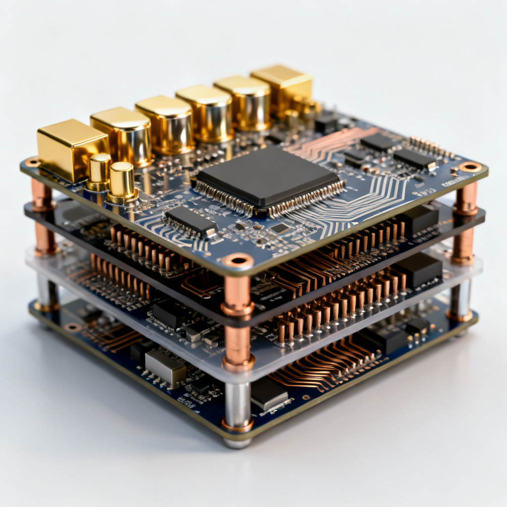
The backbone of AI is the data center, and the heart of the AI server is the PCB. AI servers, particularly those housing NVIDIA’s H100/B100 GPUs or AMD’s MI300X, require significantly more complex PCBs than traditional servers.
- Key Requirement: High-Density Interconnect (HDI) PCBs, especially Any-Layer HDI. These boards use sequential lamination and stacked microvias to route the massive number of signals between the GPU, CPU, and high-bandwidth memory (HBM).
- Layer Count Explosion: AI server main boards are moving from 16-20 layers to 24-30+ layers, with some designs exceeding 40 layers. This requires extremely precise impedance control (e.g., 85Ω ± 5%) and low signal loss.
- Material Evolution: Standard FR-4 is insufficient. We see a mass adoption of low-loss and ultra-low-loss materials like MEGTRON6, GETEK, and PTFE-based laminates to handle data rates of 112 Gbps PAM4 and beyond. These materials are critical for maintaining signal integrity over longer traces on large backplanes.
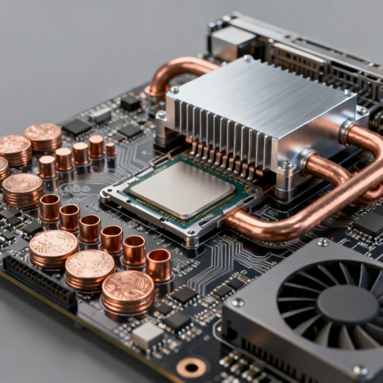
- Thermal Management: AI chips can draw 700W+ per GPU. PCBs must incorporate advanced thermal solutions like embedded copper coins, thick copper layers (3oz to 6oz), and thermal vias to dissipate heat effectively, preventing performance throttling and failure.
Edge AI: The Rise of Compact, Ruggedized PCBs
While cloud AI is massive, Edge AI is explosive. This involves running AI algorithms locally on devices like smartphones, IoT sensors, industrial robots, and autonomous vehicles.
- Miniaturization: Edge AI devices demand extremely compact form factors. This drives the need for ultra-HDI PCBs with lines and spaces down to 30μm/30μm (and moving towards 20μm/20μm) and microvias of 75μm diameter.
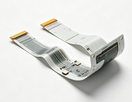
- Rigid-Flex Integration: To fit complex electronics into tight, moving enclosures (e.g., robotic arms, drones), rigid-flex PCBs are becoming the standard. They eliminate connectors, save space, and improve reliability under vibration.
- Low Power, High Performance: PCBs for edge AI must support low-power processors while maintaining high-speed data transfer for real-time decision-making. This requires careful material selection to balance cost, performance, and power consumption.
Network Infrastructure Backbone
AI workloads are not just in servers; they are in the network. The switches, routers, and optical transceivers that connect data centers require the most advanced PCBs on the market.
- High-Speed Backplanes: These massive boards (often 30″ x 40″) require extremely tight impedance control and low insertion loss to support 800G and 1.6T Ethernet standards.
- Advanced Materials for Optical Modules: PCBs for 400G and 800G optical modules use high-frequency materials like Rogers 4350B or Panasonic Megtron 7N. These boards often feature hybrid constructions, combining standard FR-4 with high-frequency laminates to manage cost while ensuring performance in the signal path.
Actionable Insight for B2B Buyers (AI)
When sourcing PCBs for AI applications, prioritize suppliers with proven capability in: Any-Layer HDI manufacturing; ultra-low-loss material lamination (e.g., MEGTRON, GETEK); advanced thermal management (copper coin, thick copper); high-layer-count (24+) production; and rigorous impedance and signal integrity testing.
Electric Vehicle (EV) Revolution: Power, Reliability, and Thermal Challenges
The automotive industry’s shift to electric vehicles is a massive driver for PCB industry trends 2025–2030, but the requirements are fundamentally different from AI. Here, the focus is on high power, high voltage, extreme reliability, and thermal dissipation over high-speed logic.
Dominance of Heavy Copper and IMS PCBs
EVs are power electronics. The traction inverter, DC-DC converter, and on-board charger (OBC) handle hundreds of volts and hundreds of amps.
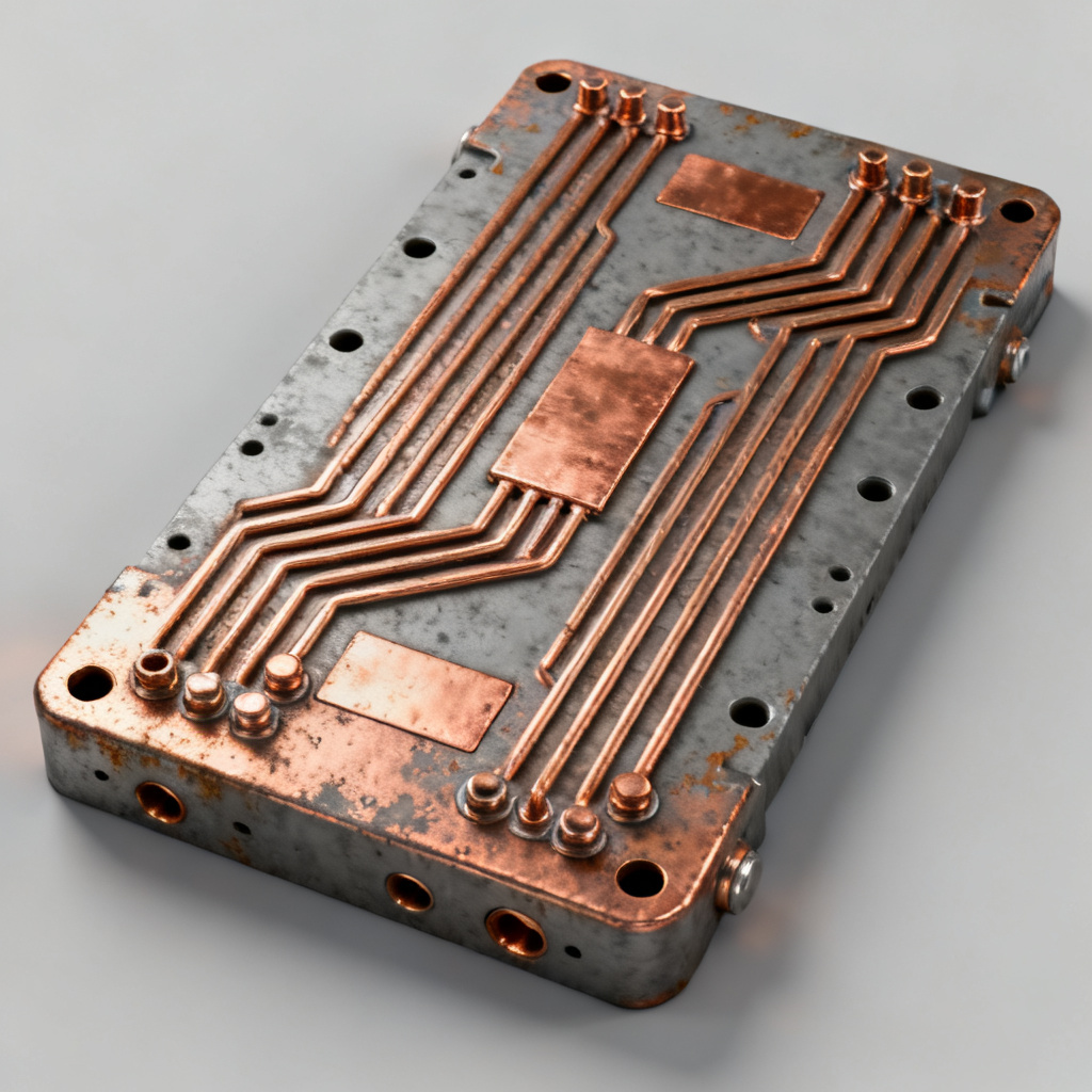
- Heavy Copper PCBs: Standard 1oz copper is insufficient. EV power stages require 4oz, 6oz, or even 10oz+ copper layers to carry high currents without excessive heat generation. These boards require specialized etching and lamination processes to avoid undercut and delamination.
- Insulated Metal Substrate (IMS) PCBs: For LED headlights and high-power modules, IMS PCBs (typically aluminum or copper base with a thin dielectric layer) are essential. They offer superior thermal conductivity, directly conducting heat from components to a heatsink.
- Thick Copper Thermal Management: Many EV PCBs now embed thick copper blocks (copper inlay) directly into the board to act as thermal bridges from hot components to the chassis or cooling plate.
Reliability in Harsh Environments
An EV is a high-stress environment with constant vibration, wide temperature swings (-40°C to +150°C), and exposure to moisture and chemicals.
- High-Tg Materials: PCBs must use FR-4 with a high glass transition temperature (Tg > 170°C) or high-performance polyimide to withstand the thermal cycling of power electronics.
- CAF Resistance: Conductive Anodic Filament (CAF) growth is a major failure mechanism in high-voltage boards. Suppliers must use CAF-resistant resin systems and control drilling quality to prevent ion migration.
- Automotive Grade Standards: PCBs must meet AEC-Q100 (component) and IPC-6012DA (automotive) qualifications. This requires 100% electrical testing, microsection analysis, and rigorous cleanliness testing (e.g., ionic contamination).
Role of HDI in Infotainment and ADAS
While the powertrain uses heavy copper, the rest of the EV is a mobile data center.
- Advanced Driver-Assistance Systems (ADAS): LIDAR, RADAR, and camera modules rely on HDI PCBs with high-frequency materials (e.g., Rogers RO3003) for radar antennas and high-layer-count rigid-flex boards for camera modules.
- Centralized E/E Architecture: New EV platforms are moving to a centralized computing model (e.g., Tesla’s HW4.0). This requires large, high-layer-count (16-22 layers) motherboards with embedded components to consolidate dozens of ECUs into one powerful computer.
- Flex and Rigid-Flex for Space: The complex, space-constrained interior of an EV (e.g., dashboard, door modules, battery management system) heavily uses flexible circuits and rigid-flex boards to route signals around moving parts and tight corners.
Actionable Insight for B2B Buyers (EV)
For EV applications, vet potential PCB suppliers for: heavy copper capability (4oz to 20oz); IMS and thick copper inlay processes; automotive certifications (IATF 16949, IPC-6012DA); high-reliability testing (thermal cycling, CAF testing, vibration); and material expertise for both power and RF applications.
Advanced Packaging: The Convergence of PCB and Semiconductor Technologies
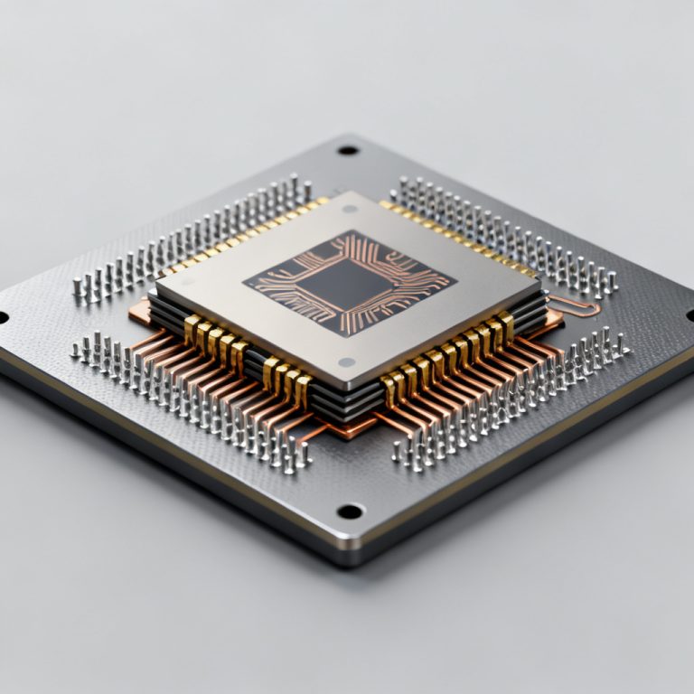
The lines between the PCB and the semiconductor package are blurring. Advanced packaging techniques are creating new interconnect layers that look and function like miniature, high-performance PCBs. This trend is crucial for PCB industry trends 2025–2030, especially for AI, high-performance computing (HPC), and 5G.
Rise of Substrate-like PCBs (SLP) and mSAP
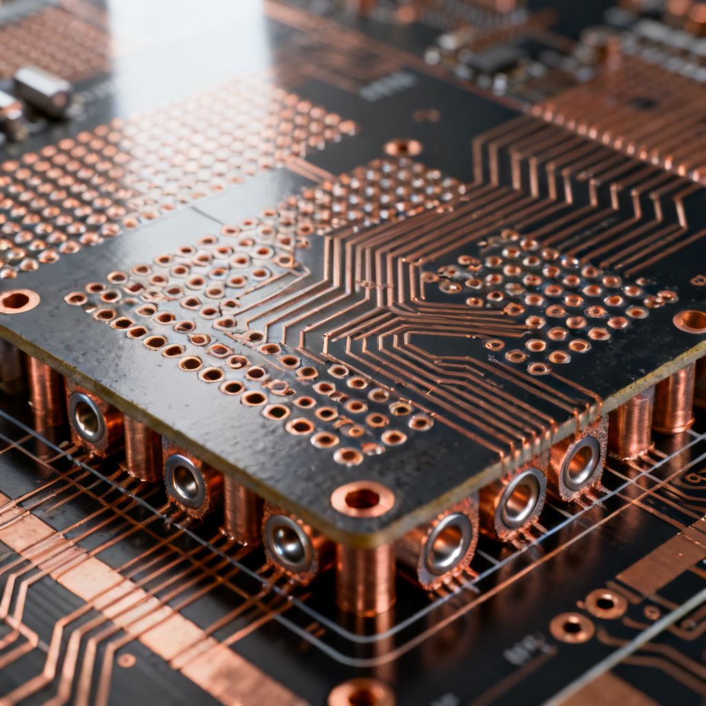
Mobile phones and high-end consumer devices have driven the need for Substrate-like PCBs (SLP). This technology uses a modified semi-additive process (mSAP) to create extremely fine lines and spaces (down to 30μm/30μm or less) on a standard PCB substrate.
- The Bridge to IC Substrates: SLP bridges the gap between traditional PCBs and high-end IC substrates (used for CPU/GPU packaging). It allows for higher routing density in a smaller area, enabling thinner, more powerful phones and laptops.
- mSAP Technology: Instead of etching away copper, mSAP deposits copper only where needed. This allows for finer features, better impedance control, and higher circuit density without the cost of IC substrate technology.
- Impact on PCB Manufacturers: This trend forces traditional PCB manufacturers to invest in semiconductor-like manufacturing capabilities, including advanced plating lines, laser drilling for microvias, and ultra-clean environments.
Embedded Component Technology (ECT)
The ultimate form of miniaturization is embedding passive and active components directly inside the PCB substrate.
- Embedded Passives: Resistors and capacitors are buried in the PCB layers. This frees up surface area for active components, reduces parasitic inductance, and improves electrical performance, especially for high-speed signals.
- Embedded Active Components: While more challenging, embedding thin ICs (e.g., power management ICs) into the PCB is gaining traction. This provides the shortest possible interconnect path, dramatically improving thermal and electrical performance.
- Application: ECT is critical for miniaturized IoT devices, medical implants, and high-reliability aerospace systems. It is also being explored for power modules in EVs to reduce size and improve thermal management.
Future: 3D IC Integration and Glass Core Substrates
Looking towards 2030, the PCB industry is preparing for the next frontier.
- 3D Packaging Implications: While 3D chip stacking happens at the IC level (using TSVs), the PCB below it must evolve. This leads to the need for very large, extremely flat, and ultra-low-loss PCBs to support multi-chip modules (MCMs) and chiplets.
- Glass Core Substrates (GCS): Intel, Samsung, and others are developing glass core substrates for IC packaging. Glass offers superior dimensional stability, lower CTE (coefficient of thermal expansion) matching with silicon, and better signal integrity at high frequencies. While initially for IC packages, this technology will inevitably trickle down to advanced PCBs for high-end networking and AI servers.
- Optical Interconnects on PCBs: To overcome the bandwidth limitations of copper, we are seeing early adoption of optical waveguides embedded in the PCB. This allows for terabit-level data transfer with almost no signal loss, a key requirement for future AI and 6G networks.
Actionable Insight for B2B Buyers (Advanced Packaging)
For advanced packaging applications, look for PCB partners investing in: mSAP and SLP production lines; embedded component technology (both passive and active); close collaboration with OSATs (Outsourced Semiconductor Assembly and Test) and chip designers; and R&D in next-generation substrates (glass core, optical PCBs).
PCB Specification Comparison: AI vs. EV vs. Advanced Packaging
| Specification | PCB for AI Applications | PCB for EV Applications | PCB for Advanced Packaging |
|---|---|---|---|
| Layer Count | 24-40+ layers | 4-16 layers | 10-30+ layers (SLP) |
| Copper Weight | 1-6oz | 4-20oz | 0.5-2oz |
| Material Type | Low-loss (MEGTRON, GETEK) | High-Tg FR-4, Polyimide | mSAP-compatible, Glass Core |
| Key Feature | Impedance control, thermal vias | Heavy copper, CAF resistance | Fine line/space, embedded components |
| Primary Standard | IPC-6012, IPC-4103 | IPC-6012DA, AEC-Q100 | IPC-6012, IPC-6018 |
FAQ: PCB Industry Trends 2025–2030
What are the key PCB industry trends 2025–2030?
How does AI impact PCB industry trends 2025–2030?
What PCB types are critical for EV industry trends 2025–2030?
What is advanced packaging in PCB industry trends 2025–2030?
How should B2B buyers prepare for PCB industry trends 2025–2030?
Conclusion: Strategic Sourcing for the 2025–2030 PCB Landscape
The PCB industry from 2025 to 2030 will be defined by specialization. A single “general-purpose” PCB manufacturer will struggle to serve the diverse needs of AI, EV, and advanced packaging markets.
- For AI and HPC: Partner with a manufacturer focused on high-layer-count, low-loss materials, and HDI technology. Demand rigorous signal integrity testing and thermal simulation.
- For EV and Automotive: Choose a supplier with deep expertise in heavy copper, IMS, and automotive-grade reliability testing. Certifications are non-negotiable.
- For Advanced Packaging and Miniaturization: Seek a forward-thinking partner investing in mSAP, embedded components, and next-generation substrates.
Your Next Step: Are you ready to build the future? Contact our engineering team to discuss your specific PCB requirements for AI, EV, or advanced packaging projects. We offer free DFM (Design for Manufacturability) reviews and rapid prototyping for complex, high-reliability boards. Let us help you navigate the trends and turn your product vision into reality.