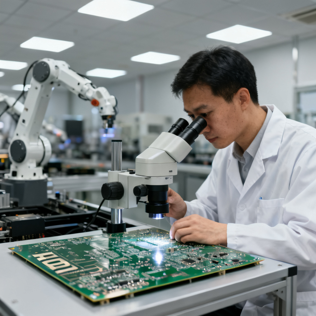
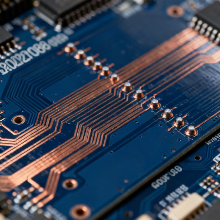
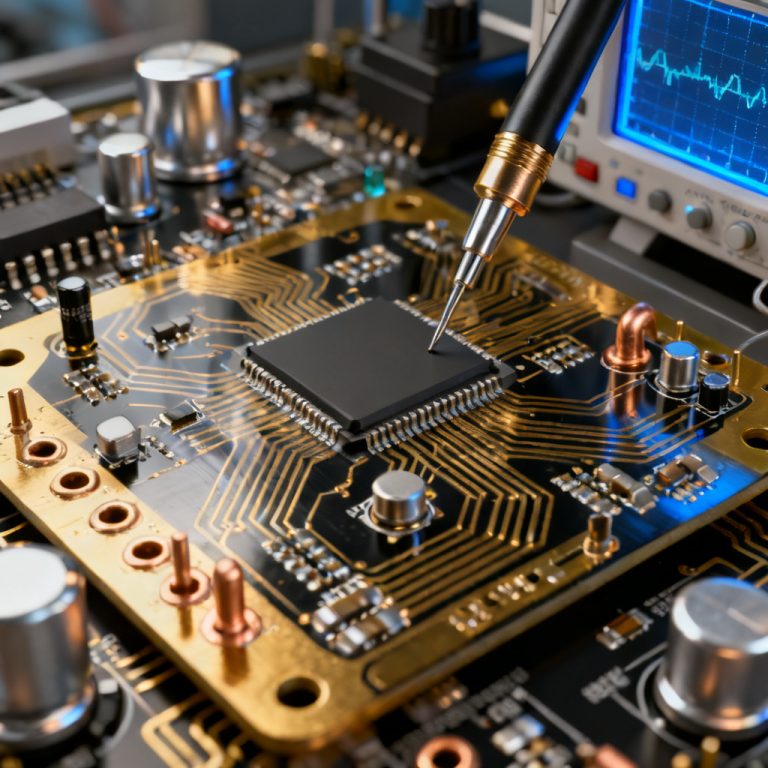
This comprehensive HDI PCB Guide Microvias Stackup and Manufacturing manual covers everything you need to know about High-Density Interconnect technology—from microvia formation and stackup design to advanced manufacturing processes. Whether you are an engineer, a procurement specialist, or a student, this resource will provide the technical depth required to make informed decisions for your next project.
What is an HDI PCB?
An HDI PCB is a printed circuit board characterized by higher wiring density per unit area compared to conventional PCBs. This is achieved through the use of finer lines and spaces (typically ≤ 100 µm), smaller vias (microvias), and higher connection pad density. HDI technology is essential for modern devices like smartphones, tablets, medical implants, and aerospace systems where space is at a premium.
Key differentiators of HDI PCB include:
- Microvias: Laser-drilled vias with diameters typically ≤ 150 µm (0.15 mm) and often as small as 50 µm.
- Buried and Blind Vias: Vias that connect only specific layers without penetrating the entire board.
- Sequential Lamination: Multiple lamination cycles to build up layers with embedded microvias.
- High Layer Count: Often up to 20+ layers in a compact form factor.
Microvias: The Heart of HDI Technology
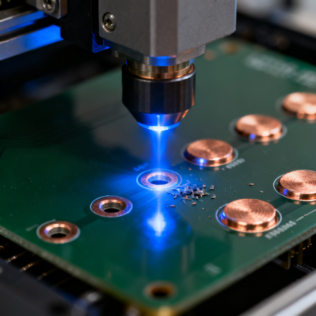
Microvias are the foundational element of HDI PCB technology. Unlike traditional mechanical drilled vias, microvias are created using laser drilling (typically CO₂ or UV lasers) and are defined by their small diameter and low aspect ratio.
Types of Microvias
- Blind Microvias: Connect an outer layer to one or more inner layers but do not go through the entire board. They are typically used for routing signals from BGA pads to inner layers.
- Buried Microvias: Located entirely within the inner layers of the PCB, connecting two or more internal layers without reaching the outer surfaces. They are formed during sequential lamination.
- Through Microvias: Rare in HDI, but some designs use microvias that go through the entire board if the thickness is extremely low (e.g., ≤ 0.4 mm).
Microvia Geometry and Aspect Ratio
The aspect ratio of a microvia is the ratio of its depth to its diameter. For reliable plating, the aspect ratio should be ≤ 1:1 for standard HDI PCB, although advanced processes can achieve up to 1.5:1. A high aspect ratio leads to uneven copper deposition, voids, and reliability issues.
| Microvia Type | Diameter | Depth | Aspect Ratio |
|---|---|---|---|
| Standard Microvia | 100 µm | 100 µm | 1:1 |
| High Aspect Ratio Microvia | 75 µm | 112 µm | 1.5:1 |
Microvia Stacking and Staggering
Microvias can be arranged in two primary configurations:
- Staggered Microvias: Microvias are offset from one layer to the next. This is the most common and reliable configuration because it distributes stress and avoids copper pillar formation.
- Stacked Microvias: Microvias are placed directly on top of each other across multiple layers. This provides the highest density but requires careful design to manage thermal stress and ensure reliable copper filling. Stacked microvias are often filled with copper (via filling) to improve mechanical strength and thermal conductivity.
Important: Stacked microvias should be limited to 2–3 layers deep to avoid reliability risks. For deeper stacks, consider using staggered patterns or copper-filled vias with controlled depth.
HDI PCB Stackup Design
The stackup of an HDI PCB is more complex than a standard multilayer board. It typically involves multiple lamination cycles, where inner layers are built up sequentially with microvia layers.
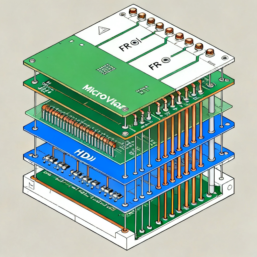
Common HDI Stackup Types (IPC-2226 Classification)
- Type I (1+N+1): One sequential lamination cycle. Core layers with one microvia layer on each side. Microvias are blind or buried. This is the simplest and most cost-effective HDI structure.
- Type II (1+N+1 with buried vias): Similar to Type I but includes at least one buried via layer in the core. This adds routing flexibility.
- Type III (2+N+2): Two sequential lamination cycles. Two microvia layers on each side of the core. This provides higher density and is common in complex mobile devices.
- Type IV (3+N+3): Three sequential lamination cycles. Used in ultra-high-density designs like advanced smartphones and servers.
- Type V (Any layer HDI): Uses conductive paste or advanced laser processes to allow microvias to connect any layer directly, eliminating the need for sequential lamination. This is the most advanced and expensive type.
Stackup Design Guidelines
- Core Thickness: Use thin core materials (≥ 0.1 mm) to reduce overall board thickness and improve microvia aspect ratio.
- Prepreg Selection: Choose high-flow or low-flow prepregs depending on whether you need to fill gaps or maintain flatness. Low-flow prepreg is preferred for microvia layers to prevent resin bleed.
- Symmetry: Always maintain symmetrical stackup to prevent warpage. For example, if you use a 2+N+2 stackup on the top, mirror it on the bottom.
- Impedance Control: HDI stackups often require tight impedance tolerances (±5%). Use controlled dielectric materials (e.g., Rogers, Isola, or high-performance FR-4) and adjust trace width and spacing accordingly.
- Layer Count Planning: For designs with 10+ layers, consider using multiple HDI build-up layers (e.g., 2+N+2) rather than a single thick core to reduce via depth.
Manufacturing Process of HDI PCBs
HDI PCB manufacturing is more complex than standard PCB fabrication due to the use of laser drilling, sequential lamination, and advanced plating. Below is the step-by-step process.
Step 1: Inner Layer Imaging and Etching
Standard inner layer processing begins with copper-clad laminate. The circuit pattern is transferred using photoresist and UV exposure, then etched to remove unwanted copper. For HDI PCB, the line width and spacing are often ≤ 75 µm, requiring high-resolution imaging (laser direct imaging or LDI) and precise etching control.
Step 2: Laser Drilling of Microvias
After inner layer etching, the next step is to drill microvias. This is done using a CO₂ laser (for larger microvias, >100 µm) or a UV laser (for smaller microvias, <75 µm). The laser ablates the dielectric material, stopping at the copper pad below.
- CO₂ Laser: Faster, good for standard microvias (100–150 µm). Requires a copper pad on the target layer.
- UV Laser: More precise, can drill smaller microvias (50–75 µm) and can also drill through copper foil (for via-in-pad applications).
Important: The target pad diameter should be at least 50 µm larger than the microvia diameter to ensure reliable capture.
Step 3: Desmear and Cleaning
After laser drilling, the hole walls contain resin residue (smear). A desmear process using plasma or chemical treatment removes this residue to ensure good adhesion for subsequent plating.
Step 4: Electroless Copper Plating
A thin layer of copper (0.5–1.0 µm) is deposited on the hole walls using electroless plating. This creates a conductive seed layer for subsequent electroplating.
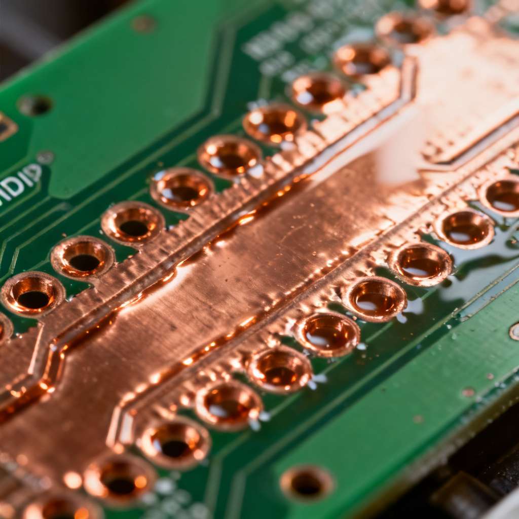
Step 5: Electrolytic Copper Plating (Via Filling)
For stacked microvias or via-in-pad designs, vias are often filled with copper using special plating chemistry. This process, called via filling, ensures that the via is completely filled with copper, providing a flat surface for subsequent layers and improving thermal management. For blind microvias that are not stacked, standard conformal plating (copper only on the walls) is sufficient.
Step 6: Sequential Lamination
This is the most critical step for HDI PCB. The board is built up layer by layer. For example, in a 2+N+2 stackup:
- First, the core (N layers) is fabricated.
- Then, a prepreg and copper foil are laminated onto the core.
- Microvias are drilled and plated on this new layer.
- This process is repeated for the second build-up layer.
Each lamination cycle requires precise temperature and pressure control to avoid resin voids and delamination.
Step 7: Outer Layer Imaging and Etching
After all build-up layers are complete, the outer layers are imaged and etched. This includes the final circuit pattern, pads, and solder mask.
Step 8: Solder Mask and Surface Finish
Standard solder mask is applied, but for HDI PCB with fine-pitch components (e.g., 0.4 mm BGA), a liquid photoimageable (LPI) solder mask is used. Surface finishes like ENIG (Electroless Nickel Immersion Gold) or ENEPIG (Electroless Nickel Electroless Palladium Immersion Gold) are preferred for HDI due to their flatness and wire bondability.
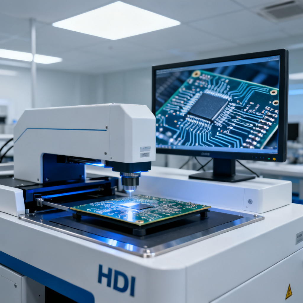
Step 9: Electrical Testing and Inspection
HDI PCB boards require rigorous testing:
- Automated Optical Inspection (AOI): Checks for shorts, opens, and misregistration.
- X-ray Inspection: Verifies microvia alignment and detects voids in filled vias.
- Impedance Testing: Ensures controlled impedance meets specifications.
- Microsectioning: Destructive testing to verify plating thickness, via fill quality, and layer alignment.
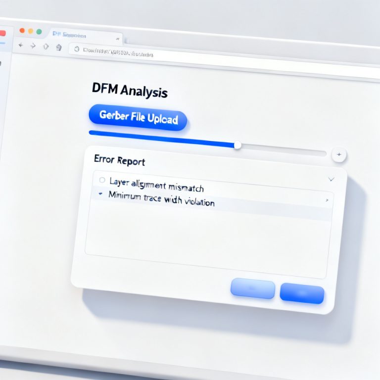
Design for Manufacturing (DFM) for HDI PCBs
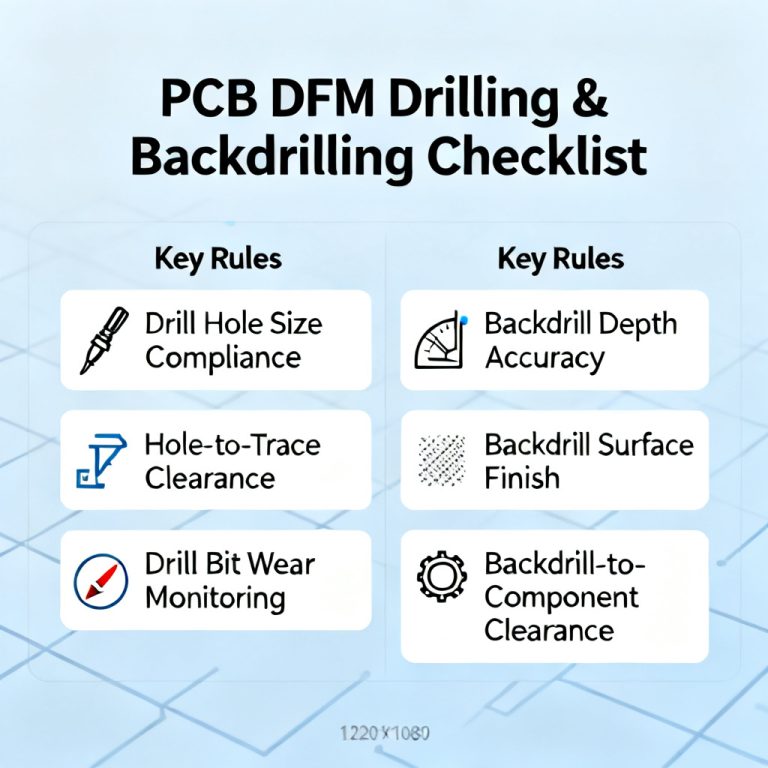
To ensure high yield and reliability, follow these DFM rules for your HDI PCB design:
- Microvia Diameter: Keep microvia diameter ≥ 100 µm for standard processes. For advanced designs, consult your manufacturer for minimum capabilities (often 75 µm).
- Microvia Pitch: Minimum pitch between microvias should be ≥ 200 µm (center-to-center) to avoid drilling into adjacent vias.
- Via-in-Pad: If placing microvias directly under BGA pads, ensure the via is filled and planarized. Unfilled vias can cause solder voids and reliability issues.
- Annular Ring: For blind microvias, the annular ring (copper pad surrounding the via) should be at least 25 µm on the target layer.
- Layer Registration: Sequential lamination requires tight registration (±25 µm). Use fiducial marks on each layer to align during lamination.
- Dielectric Thickness: Thinner dielectrics (≤ 50 µm) are preferred for microvia layers to reduce aspect ratio and improve drilling quality.
Common HDI PCB Applications
- Consumer Electronics: Smartphones, tablets, wearables (e.g., Apple iPhone, Samsung Galaxy).
- Medical Devices: Hearing aids, pacemakers, diagnostic imaging equipment.
- Automotive: Advanced driver-assistance systems (ADAS), infotainment, engine control units.
- Aerospace and Defense: Satellite communication, radar systems, avionics.
- Telecommunications: 5G base stations, network switches, high-speed routers.
Cost Considerations
HDI PCB are more expensive than standard multilayer boards due to:
- Additional lamination cycles: Each build-up layer adds cost.
- Laser drilling: Slower than mechanical drilling.
- Via filling: Specialized plating chemistry and equipment.
- Tight tolerances: Higher scrap rate and more inspection.
Cost-saving tips:
- Use Type I (1+N+1) stackup when possible.
- Avoid unnecessary microvia stacking.
- Optimize panel utilization (e.g., use standard panel sizes like 18″ x 24″).
- Choose standard materials (e.g., FR-4 high-Tg) unless high-frequency performance is required.
Comparison: HDI PCB vs Standard PCB
| Feature | HDI PCB | Standard PCB |
|---|---|---|
| Via Type | Microvias (blind/buried/stacked) | Through-hole vias |
| Line Width/Space | ≤ 100 µm | ≥ 150 µm |
| Layer Count | Up to 20+ layers | Typically 2–10 layers |
| Lamination Cycles | Multiple sequential cycles | Single lamination |
| Cost | Higher | Lower |
| Application | Miniaturized, high-speed devices | General electronics |
Frequently Asked Questions about HDI PCB
What is the main advantage of using an HDI PCB?
The main advantage of an HDI PCB is its ability to accommodate higher component density and finer pitch devices, enabling miniaturization and improved signal integrity in compact electronic products.
How are microvias created in HDI PCB manufacturing?
Microvias in HDI PCB manufacturing are created using laser drilling (CO₂ or UV lasers), which precisely ablates the dielectric material to form small, reliable vias for layer interconnection.
What is the difference between staggered and stacked microvias?
Staggered microvias are offset between layers for better reliability, while stacked microvias are placed directly on top of each other for highest density. Stacked microvias require copper filling and are limited to 2–3 layers deep in HDI PCB designs.
What stackup type is most cost-effective for HDI PCBs?
Type I (1+N+1) stackup is the most cost-effective HDI PCB structure, involving one sequential lamination cycle with microvias on each side of the core.
Why is via filling important in HDI PCBs?
Via filling is crucial in HDI PCB because it provides a flat surface for subsequent layers and BGA pads, improves thermal management, and enhances mechanical reliability for stacked microvias.
Conclusion
HDI PCB technology is essential for modern high-density electronics. By understanding microvia types, stackup design, and manufacturing processes, you can design reliable, cost-effective boards that meet the demands of today’s miniaturized devices. Always collaborate closely with your HDI PCB manufacturer during the design phase to ensure your design is manufacturable and cost-efficient.
For a free DFM review or to request a quote for your HDI PCB project, contact our engineering team today. We specialize in HDI fabrication with capabilities down to 50 µm microvias, 2+N+2 stackups, and advanced via filling.