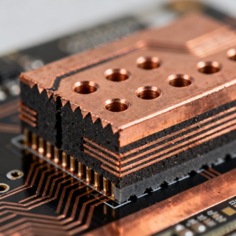
Thick Copper PCB Guide 3oz up to 20oz Design Current Capacity
This comprehensive Thick Copper PCB Guide 3oz up to 20oz Design Current Capacity manual covers everything from copper weight ranges to specialized DFM rules, current-carrying charts, and manufacturing challenges. Whether you are designing for power supplies, automotive systems, or renewable energy, this heavy copper technical resource helps you achieve reliable, high-performance results.
What is a Thick Copper PCB?
Definition and Copper Weight Range
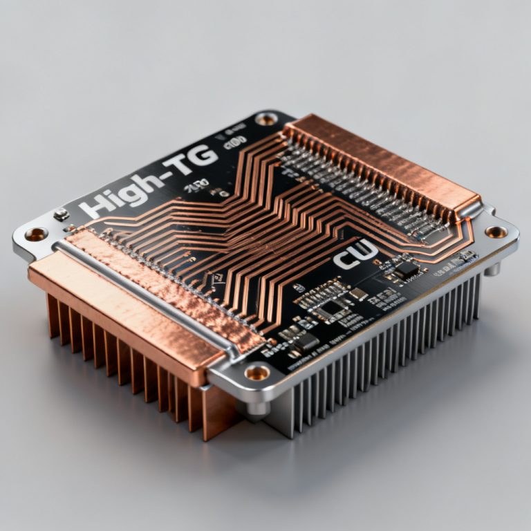
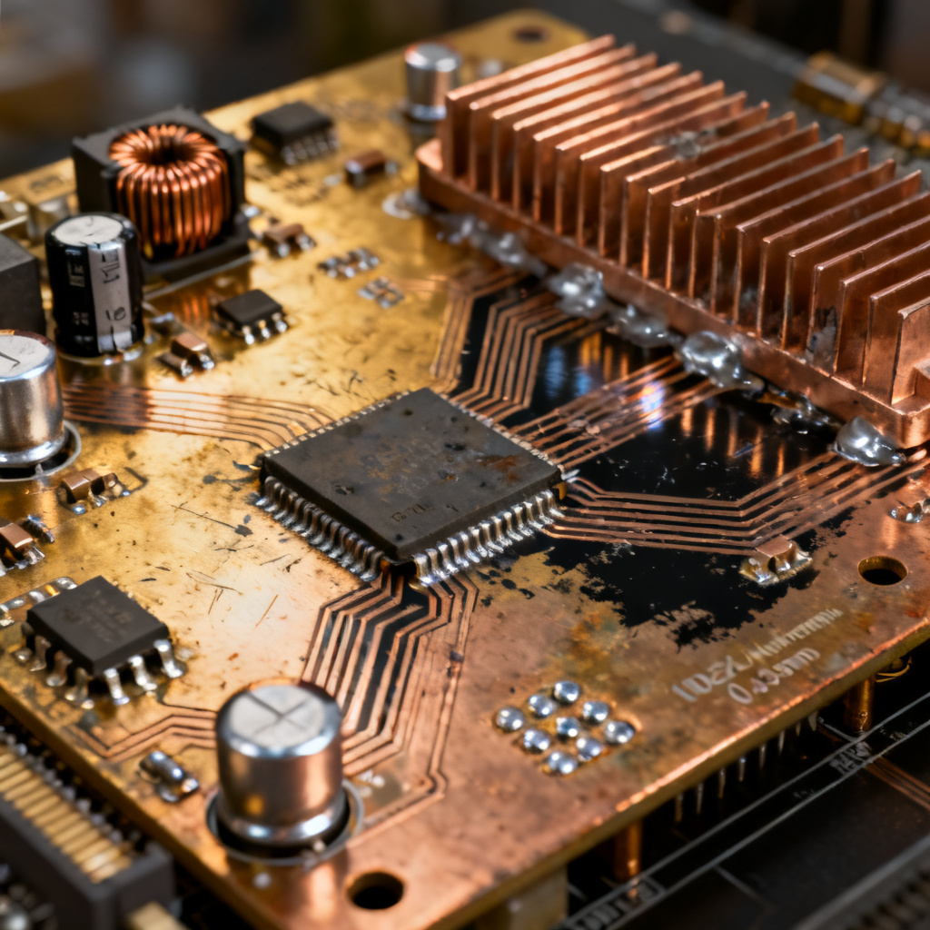
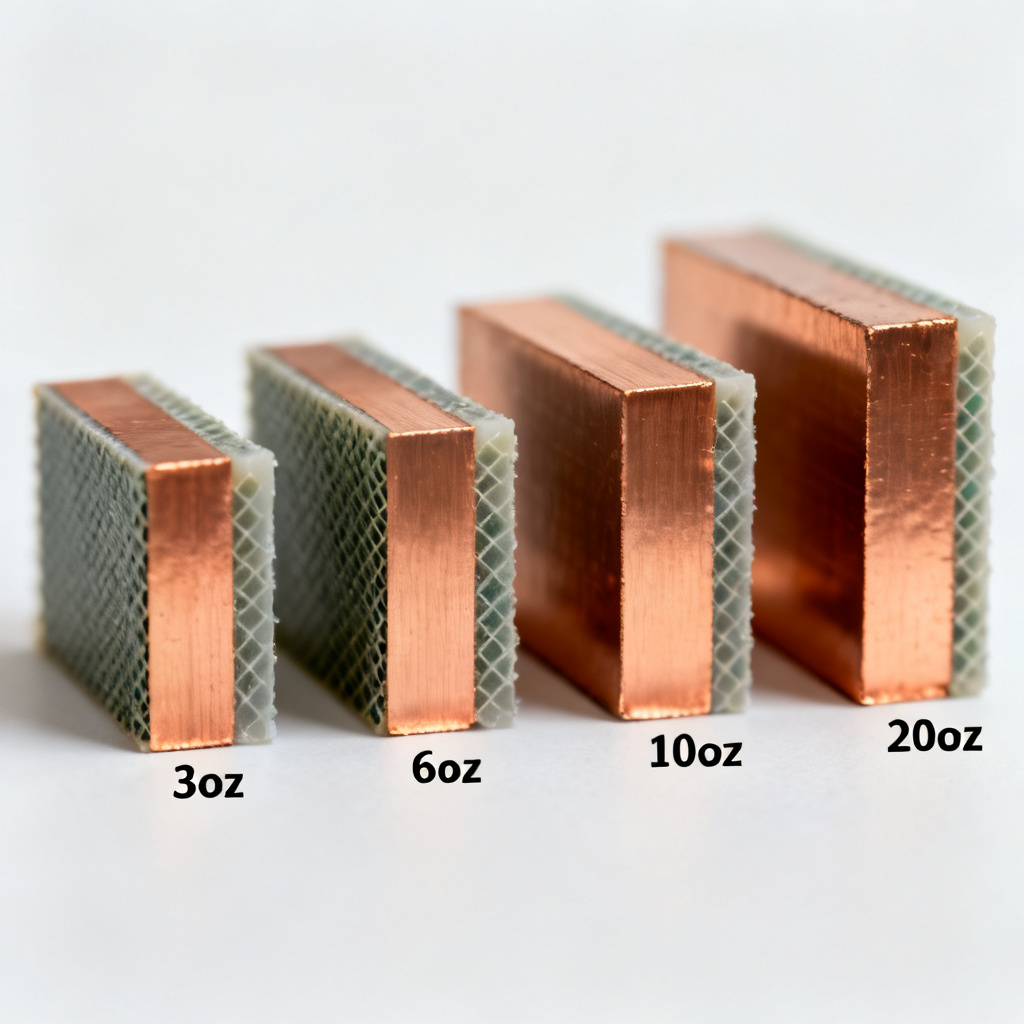
A thick copper PCB is defined by its copper foil thickness exceeding standard 1oz or 2oz. Typically, thick copper starts at 3oz (approximately 105µm or 4.2 mils) and extends up to 20oz (700µm or 28 mils). Some manufacturers can push beyond 20oz for specialized applications, but 3oz to 20oz covers the vast majority of industrial needs.
Why Choose Thick Copper?
- High Current Capacity: Thicker copper traces reduce resistance, allowing higher current flow without overheating. For example, a 3oz trace can carry significantly more current than a 1oz trace of the same width.
- Superior Thermal Management: Copper is an excellent heat conductor. Thick copper layers dissipate heat more effectively, preventing hot spots and extending component lifespan.
- Mechanical Strength: Thicker copper provides greater structural integrity, especially in boards subjected to vibration or thermal cycling.
- Lower Voltage Drop: For power distribution circuits, thick copper minimizes voltage drop over long traces.
Common Applications
- Power Supplies: AC/DC converters, inverters, and UPS systems rely on thick copper for high current paths.
- Automotive Electronics: Electric vehicle (EV) battery management systems, motor controllers, and LED lighting modules.
- Industrial Equipment: Motor drives, welding machines, and power distribution panels.
- Renewable Energy: Solar inverters and wind turbine controllers.
- Telecommunications: Base station power amplifiers and high-frequency RF circuits requiring low resistance.
Design Considerations for Thick Copper PCBs
Designing for thick copper PCBs is fundamentally different from standard PCBs. The increased copper thickness impacts trace geometry, spacing, and manufacturing processes. Here are the key design parameters you must address.
Trace Width and Current Capacity
The relationship between trace width, copper thickness, and current capacity is governed by IPC-2221 standards (and its predecessor IPC-2222). For thick copper, the standard formulas still apply but require adjustments.
- IPC-2221 Formula: Current (I) = k * (Temperature Rise)^0.44 * (Trace Width)^0.725 * (Copper Thickness)^0.725, where k is a constant (0.024 for inner layers, 0.048 for outer layers).
- Practical Example: For a 10°C temperature rise on an outer layer:
- 3oz copper, 100 mil trace width: ~6A
- 6oz copper, 100 mil trace width: ~10A
- 10oz copper, 200 mil trace width: ~20A
- 20oz copper, 500 mil trace width: ~50A
- Note: These are approximations. Always use a PCB current calculator or consult your manufacturer for precise values, as factors like ambient temperature and airflow matter.
Minimum Trace Width and Spacing
Thick copper requires wider minimum trace widths and spacing due to etching limitations.
- 3oz to 6oz: Minimum trace width/spacing is typically 8-10 mils (0.2-0.25mm). For complex designs, 12 mils is safer.
- 10oz to 20oz: Minimum trace width/spacing jumps to 20-40 mils (0.5-1.0mm). Narrower traces risk under-etching or over-etching during manufacturing.
- Spacing for High Voltage: For safety, maintain at least 0.5mm per 100V of potential difference. Thick copper can exacerbate creepage issues, so increase clearance accordingly.
Via Design and Thermal Management
Vias in thick copper PCBs must be robust to handle current and thermal stress.
- Via Diameter: For 3-6oz copper, use a minimum finished hole diameter of 0.3mm (12 mils). For 10-20oz, increase to 0.5mm (20 mils) or larger.
- Via Wall Thickness: Standard plated through-hole (PTH) copper thickness is 1oz (35µm). For high-current vias, consider sequential lamination or filling with conductive epoxy to thicken via walls.
- Thermal Reliefs: Use thermal relief pads for components connected to large copper planes. For thick copper, a spoke width of at least 10 mils (0.25mm) is recommended to ensure solderability.
Layer Stackup and Material Selection
Thick copper layers affect the overall stackup and material choices.
- Core vs. Prepreg: For inner layers, use thick copper foil laminated onto a core. For outer layers, additional copper plating is applied after drilling.
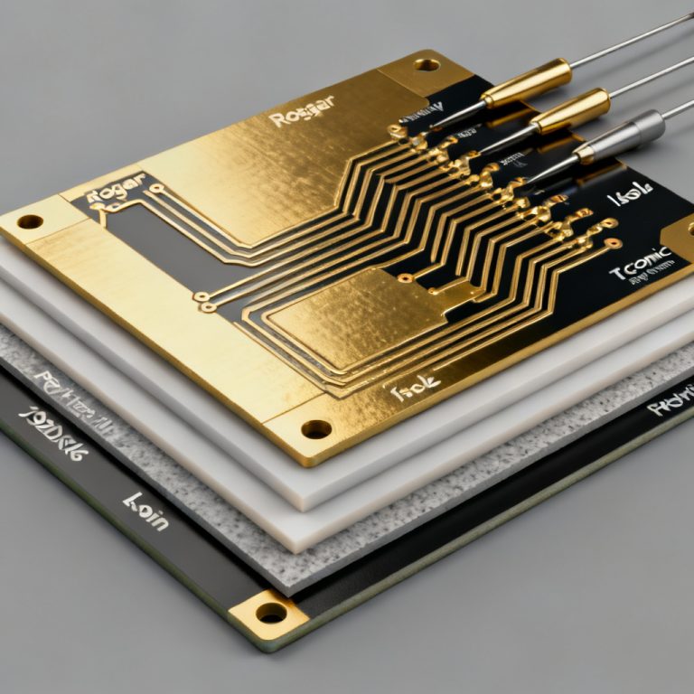
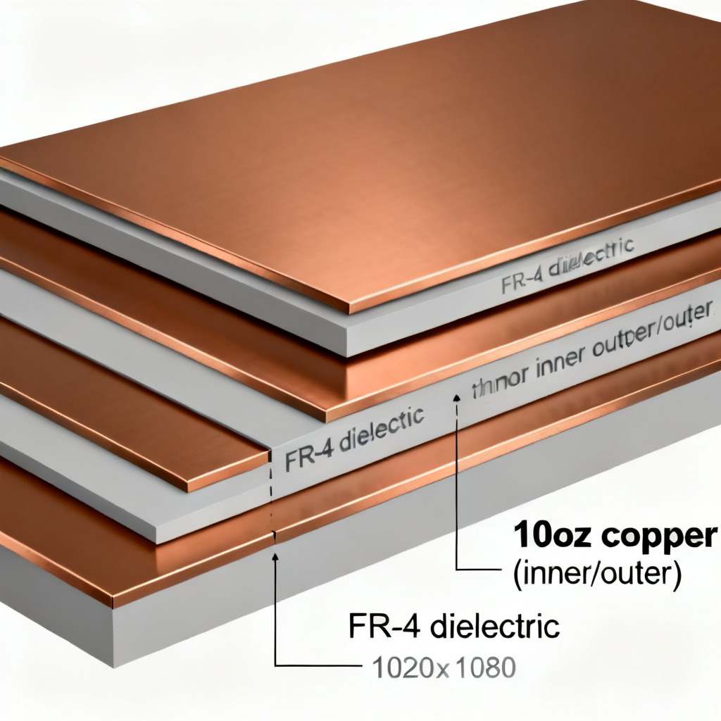
- Dielectric Materials: Standard FR-4 is suitable for up to 6oz, but for 10oz and above, high-Tg (glass transition temperature) materials like FR-4 High Tg (170°C+) or polyimide are recommended to prevent delamination during thermal cycling.
- Copper Balancing: To prevent warpage, ensure symmetrical copper distribution across layers. If one layer has 10oz, the opposite layer should have similar copper weight.
Manufacturing Challenges and Solutions
Thick copper PCBs pose unique manufacturing challenges that require specialized processes. Understanding these helps you design for manufacturability (DFM).
Etching Process
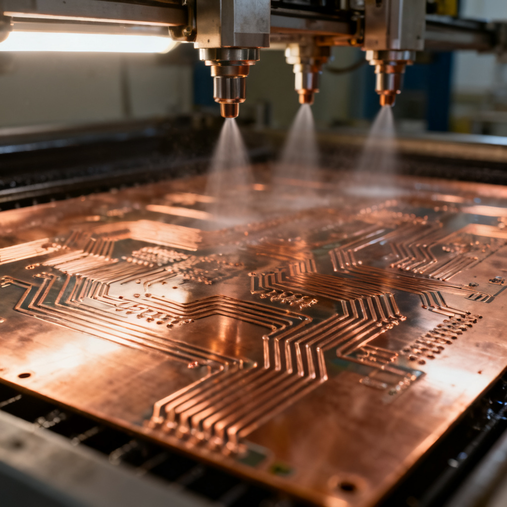
Standard etching processes struggle with thick copper because the etchant must remove more material.
- Issue: Over-etching can narrow traces, while under-etching leaves copper residue. Both cause impedance variations and potential shorts.
- Solution: Use differential etching or step-etching techniques. Some manufacturers apply multiple etching cycles with precise control. For 10oz and above, laser direct imaging (LDI) is often used for finer resolution.
Drilling
Thick copper layers make drilling harder due to the ductility of copper.
- Issue: Copper burrs can form around holes, causing short circuits or poor solderability.
- Solution: Use carbide drill bits with optimized geometries. Increase drilling speed and reduce feed rate. After drilling, deburring processes (e.g., chemical or mechanical) are critical.
Lamination and Pressing
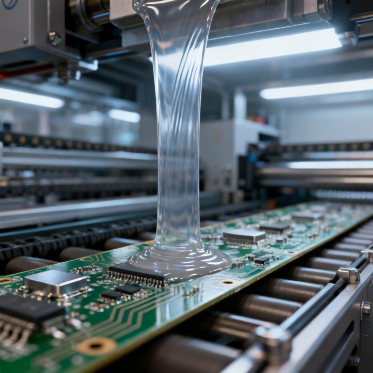
Thick copper requires higher lamination pressure and temperature to ensure proper bonding with prepreg.
- Issue: Air pockets or voids can form between copper and dielectric, leading to delamination.
- Solution: Use vacuum lamination to remove air. For 10oz+ copper, pre-lamination baking of the copper foil helps remove moisture.
Plating
For outer layers, additional copper plating is needed to achieve target thickness.
- Process: After drilling, electroless copper is applied, followed by electrolytic copper plating. For thick copper, multiple plating cycles may be required.
- Uniformity: Thick copper plating can be uneven on edges or near holes. Use pulse plating or periodic reverse current (PRC) plating for better distribution.
Current Capacity and Thermal Performance
Accurate current capacity estimation is critical for thick copper PCBs. This chapter provides detailed data and practical guidelines.
Current Capacity Table (Outer Layer, 10°C Rise)
| Copper Weight (oz) | Trace Width (mils) | Current (A) |
|---|---|---|
| 3oz | 50 | 3.5 |
| 3oz | 100 | 6.0 |
| 3oz | 200 | 10.5 |
| 6oz | 50 | 5.5 |
| 6oz | 100 | 10.0 |
| 6oz | 200 | 17.5 |
| 10oz | 100 | 15.0 |
| 10oz | 200 | 26.0 |
| 10oz | 500 | 55.0 |
| 20oz | 200 | 38.0 |
| 20oz | 500 | 80.0 |
| 20oz | 1000 | 140.0 |
Note: Inner layer current capacity is roughly 50-70% of outer layer values due to poorer heat dissipation. Use a 10°C rise as a conservative target; for higher rises (e.g., 20°C), multiply current by ~1.4.
Thermal Management Strategies
- Copper Pour Areas: Use large copper pours (e.g., power planes) to spread heat. For thick copper, a 1-inch square pour can dissipate 5-10W more than a standard 1oz pour.
- Thermal Vias: Place arrays of small vias (e.g., 0.3mm diameter, 1mm pitch) under hot components to conduct heat to inner layers or a heatsink.
- Heatsinks: For extreme currents (above 50A), attach external heatsinks to the PCB using thermal interface materials (TIMs).
Cost and Lead Time Implications
Thick copper PCBs are more expensive and time-consuming to produce than standard boards. Here’s what to expect.
Cost Drivers
- Copper Weight: Costs increase exponentially with copper thickness. A 10oz PCB can be 2-3x more expensive than a 3oz one.
- Layer Count: More layers amplify costs due to additional lamination and plating steps.
- Minimum Quantities: Many manufacturers require minimum order quantities (MOQs) of 5-10 boards for thick copper, especially above 10oz.
- Special Processes: Additional steps like step-etching or vacuum lamination add 15-30% to the base cost.
Lead Times
- 3oz to 6oz: Standard lead times of 2-3 weeks.
- 10oz to 20oz: Extended lead times of 4-6 weeks due to slower etching and plating.
- Rush Orders: Expedited services (e.g., 1-2 weeks) are possible but at a 50-100% premium.
Choosing the Right Copper Weight for Your Application
Selecting the optimal copper thickness balances performance, cost, and manufacturability.
Guidelines by Application
- 3oz to 4oz: Ideal for moderate current (up to 10A) in power supplies, LED drivers, and automotive modules. Offers good thermal performance without excessive cost.
- 6oz to 8oz: Suitable for high-current applications (10-30A) like motor controllers and industrial inverters. Requires careful DFM but is widely available.
- 10oz to 16oz: Used in very high-current circuits (30-80A) such as EV battery packs and welding equipment. Manufacturing complexity increases significantly.
- 20oz: Reserved for extreme currents (80A+) in specialized equipment like railway traction systems or high-power RF amplifiers. Expect long lead times and high costs.
When to Avoid Thick Copper
- High-Density Interconnect (HDI) Designs: Thick copper limits trace width and spacing, making fine-pitch components (e.g., BGA) difficult.
- High-Frequency Circuits: Thick copper can increase skin effect losses at GHz frequencies. Use standard 1oz or 2oz for RF.
- Cost-Sensitive Projects: If current is under 5A, standard 2oz copper is more economical.
Testing and Quality Assurance
Ensuring reliability of thick copper PCBs requires rigorous testing.
Key Tests
- Continuity and Isolation: Use flying probe or fixture testing to verify trace integrity. For thick copper, test voltages should be higher (e.g., 500V) to detect micro-cracks.
- Thermal Cycling: Subject boards to -40°C to +125°C cycles (100+ cycles) to check for delamination or via cracking.
- Current Capacity Testing: Apply rated current and monitor temperature rise using thermocouples. Ensure it stays within design limits (e.g., 10°C above ambient).
- Cross-Section Analysis: Cut and polish a sample to measure actual copper thickness, via wall thickness, and laminate quality.
Common Defects to Watch For
- Under-etching: Traces are wider than designed, reducing spacing and increasing capacitance.
- Over-etching: Traces are narrower, increasing resistance and current density.
- Delamination: Copper separates from dielectric due to poor lamination.
- Burr Formation: Copper burrs around drilled holes can cause shorts.

Future Trends in Thick Copper PCB Technology
The demand for thick copper PCBs is growing with the rise of electric vehicles, renewable energy, and high-power computing.
Emerging Developments
- Embedded Copper Blocks: Instead of thick copper layers, some designs embed solid copper blocks (e.g., 1mm thick) for ultra-high current paths. This reduces overall board thickness.
- Hybrid Stackups: Combining thick copper (e.g., 10oz) with standard layers (1oz) in a single board to optimize cost and performance.
- Advanced Plating Techniques: Electroless Ni/Pd/Au (ENEPIG) or immersion silver for thick copper surfaces to improve solderability and corrosion resistance.
- Automated DFM Tools: Software like Altium Designer or Cadence now includes thick copper-specific design rules, making it easier to avoid manufacturing pitfalls.