Gerber Generation and Validation Output Settings
In B2B PCB manufacturing, mastering Gerber generation and validation output settings is the contract between your design intent and fabrication reality. Incorrect output settings or missing validation steps can lead to costly delays, scrapped prototypes, or production failures. This comprehensive pillar page consolidates authoritative industry knowledge to ensure first-pass success for reliable, high-yield PCB production.
Understanding Gerber Generation and Validation Output Settings: The Foundation
Before diving into specific Gerber generation and validation output settings, it is essential to understand the Gerber format itself. The industry standard has evolved from legacy RS-274-D to modern RS-274X (Extended Gerber or X-Gerber). The RS-274X format embeds all aperture definitions directly into the file, eliminating the need for a separate aperture list. This self-contained nature drastically reduces errors during file transfer and interpretation by PCB manufacturers.
Key characteristics of RS-274X for Gerber generation
Key characteristics of RS-274X include embedded apertures (no external aperture files required), polarity support for positive and negative layers (e.g., for copper planes), coordinate precision typically using 2:4 or 2:5 format (e.g., 2 integer digits, 4 decimal digits) ensuring micron-level accuracy, and logical layer naming (e.g., TOP_COPPER.GTL, BOTTOM_SOLDERMASK.GBS). For B2B production, most professional PCB manufacturers, including those serving high-reliability industries (military, aerospace, medical), require RS-274X format. Using legacy formats like RS-274-D or proprietary formats often leads to file rejection or additional engineering time, impacting project timeline and cost. Always set your output to RS-274X.
Critical Output Settings for Gerber Generation and Validation
The output settings you choose during Gerber generation and validation directly influence manufacturability. Below are the parameters that must be correctly configured in your PCB design software (such as Altium Designer, KiCad, Eagle, or OrCAD).
File Format and Precision
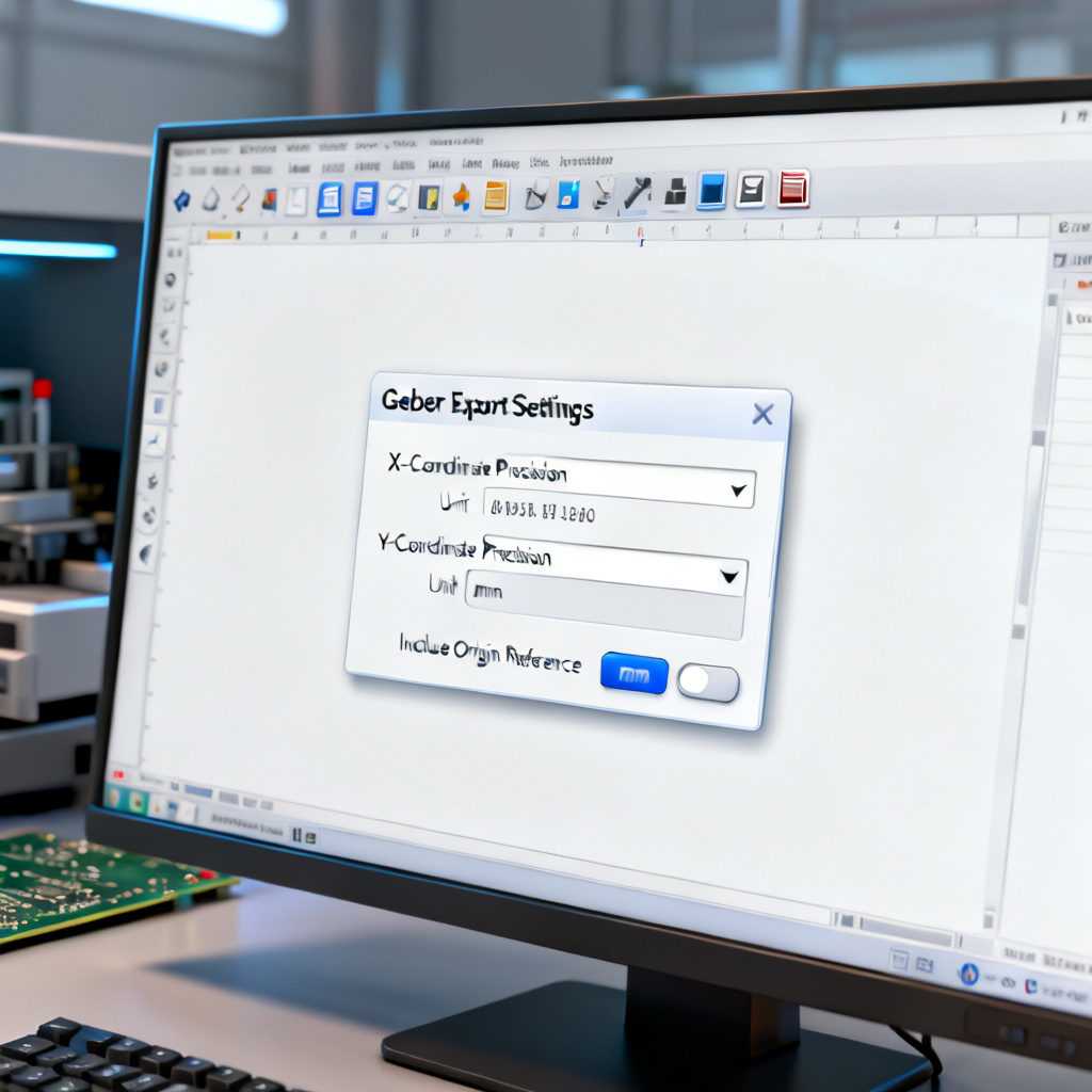
For file format and precision, select RS-274X (Extended Gerber). If your software offers Gerber X2 (a superset of RS-274X), use it for enhanced metadata (e.g., layer stackup, component information). However, ensure your manufacturer supports X2. Use coordinate precision 2:5 (2 integer digits, 5 decimal digits) or 2:4 at minimum. 2:5 provides 0.01 mil (0.25 micron) resolution, critical for fine-pitch components (e.g., BGA, QFN). Avoid 2:3 as it can cause rounding errors on small features. Set units to millimeters or inches consistently across all files. Most manufacturers prefer millimeters for metric designs. Never mix units in a single order.
Layer Mapping and Naming
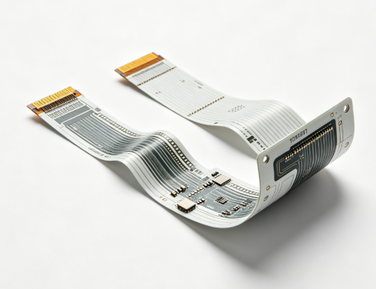
Each physical layer of your PCB requires a separate Gerber file. A standard 2-layer board needs at least 7 files: top copper (GTL), bottom copper (GBL), top solder mask (GTS), bottom solder mask (GBS), top silkscreen (GTO), bottom silkscreen (GBO), and board outline (GKO or job file). For multi-layer boards, add internal copper layers (e.g., G1, G2), internal planes, and drill files. Use consistent, descriptive naming that matches industry conventions (e.g., .GTL for top copper, .GBL for bottom copper). Avoid generic names like layer1.ger. Many manufacturers provide a Gerber file naming template; adopt it to avoid confusion.
Aperture Settings
Ensure embedded apertures are generated inside the Gerber file. Do not create a separate aperture file (.APT or .REP). Use standard aperture sizes (e.g., 0.010″, 0.020″) for traces and pads. Avoid non-standard sizes that may not be available in the manufacturer’s tool library. For pads and vias, use flashed apertures (not drawn or stroked). Flashed pads are more accurate and easier for the manufacturer to process.
Polarity and Layer Type
For copper layers (signal, power, ground), use positive polarity (dark). For solder mask, use negative polarity (clear) unless your software defaults to positive; check your manufacturer’s preference. For internal power/ground planes, you can use negative layers (copper pour with thermal relief) or positive layers with copper fills. Negative layers reduce file size but require careful thermal relief design. Most modern manufacturers prefer positive layers.
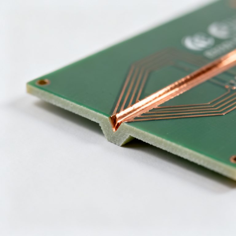
Board Outline and Cutouts
Generate a dedicated board outline file (e.g., BOARD_OUTLINE.GKO). This should be a closed contour (no gaps) with a line width of at least 0.010″ (0.254 mm). If your board has internal cutouts (slots, mounting holes), include them in the same outline file. Use a 0-width line or a dedicated “cutout” layer, depending on your software. Ensure all copper, silkscreen, and mask features are at least 0.010″ (0.254 mm) from the board edge to avoid routing issues.
Drill Files (Excellon Format)
Drill files are not Gerber but are equally critical. Generate them in Excellon 2 format (sometimes called “Excellon with file header”). Units must match your Gerber units (mm or inches). Use 2:4 or 2:5 precision. Include a tool list (diameter, tool number) in the file header. Clearly separate plated (PTH) and non-plated (NPTH) holes. Some manufacturers require separate drill files for each. For elongated slots, use a separate “routed” file or a specific slot drill file. Most manufacturers prefer slots to be drawn on the outline layer.
Netlist and IPC-356 Files (Optional but Recommended)
Generate an IPC-356 netlist file that maps all connections. This allows manufacturers to perform electrical testing (flying probe or fixture) and verify continuity. Some manufacturers accept ODB++ or IPC-2581 database formats as alternatives to Gerber. They contain all layer data, netlists, and stackup information in a single file. If your software supports it, consider exporting ODB++ for complex boards.
Gerber Validation: The Critical Step Before Sending to Production
Generating Gerber files is only half the battle. Gerber generation and validation ensures your output settings are correct and your design is manufacturable. Below are the validation steps every B2B PCB buyer or engineer should follow.

Visual Inspection Using a Gerber Viewer
Use a free or professional Gerber viewer (e.g., Gerbv, ViewMate, Altium 365 Viewer, CircuitCAM, or GC-Prevue) to open each file. Check layer alignment by overlaying all copper layers, mask, and silkscreen. Ensure they align perfectly; misalignment can cause shorts or opens. Verify the board outline is closed and matches your design intent. Look for stray lines or gaps. Inspect solder mask to ensure mask openings align with pads. Solder mask slivers (narrow mask lines) can cause manufacturing defects. Check silkscreen should not overlap pads or vias (unless intentional). Overlapping silkscreen can cause soldering issues. Open the drill file and ensure hole sizes are correct and match your design; check for missing or extra holes.
Design Rule Check (DRC) on Gerber Data
Many Gerber viewers offer DRC capabilities. Perform these checks: minimum trace width and spacing verifying your design meets the manufacturer’s capabilities (e.g., 4/4 mil trace/space for standard, 3/3 mil for advanced); annular ring ensuring pad size minus drill size is at least the manufacturer’s minimum annular ring (e.g., 5 mil for standard); solder mask clearance where mask opening should be 2-4 mil larger than the pad on each side; and copper to edge clearance where copper should be at least 10-15 mil from the board edge.
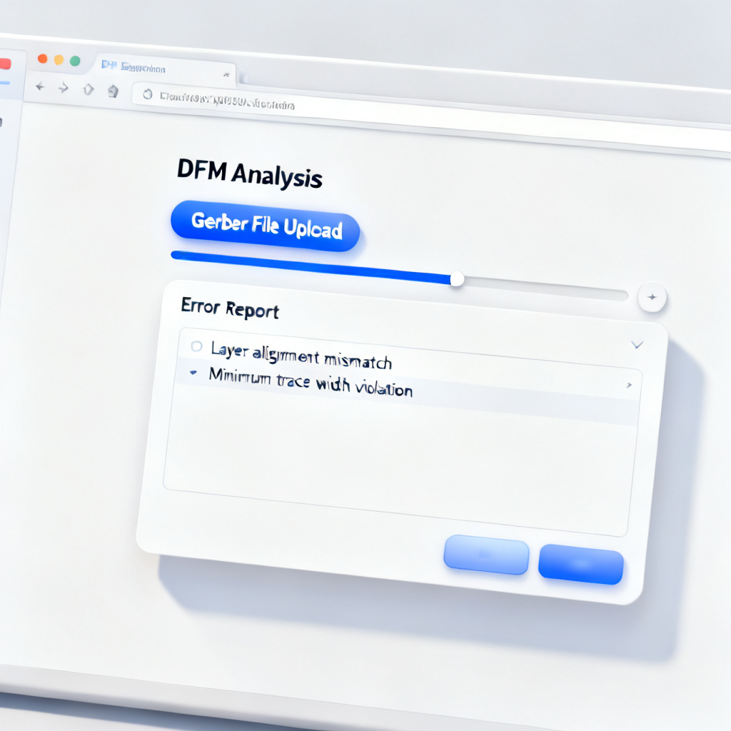
DFM (Design for Manufacturing) Analysis
Most professional PCB manufacturers offer free DFM checks. Use their online tools or software (e.g., Eurocircuits DFM, PCBWay DFM, JLCPCB DFM). These tools automatically detect missing or incomplete Gerber files, incorrect file format or precision, silkscreen on pads, acid traps (acute angles in copper traces), starved thermals (incomplete thermal relief connections), copper slivers (narrow copper islands), and hole-to-copper clearance issues. Running DFM on your generated files before submitting the order catches issues at this stage, saving days of back-and-forth communication.
Stackup and Impedance Validation
Ensure your Gerber files match the stackup specified in your order (e.g., 4-layer, 1.6mm thickness, FR4). Some manufacturers require a separate stackup document. If your design requires controlled impedance (e.g., 50 ohms), include impedance profiles in your documentation. The manufacturer will adjust trace widths and dielectric thickness to meet your target. Do not assume the Gerber files alone convey impedance requirements.
Netlist Verification
Use a tool that can extract netlists from Gerber (e.g., GC-Prevue or Fab3000) and compare them to your IPC-356 netlist. This catches open circuits or shorts that visual inspection might miss. If your volume is low to medium, request flying probe testing. This is the most reliable way to verify electrical connectivity.
Common Mistakes in Gerber Generation and Validation Output Settings
Even experienced designers make these mistakes. Awareness is the first step to prevention.
| Mistake | Consequence | Solution |
|---|---|---|
| Using RS-274-D (no embedded apertures) | File rejection; manufacturer cannot read apertures | Always use RS-274X |
| Incorrect coordinate format (e.g., 2:3) | Rounding errors on small features; misalignment | Use 2:4 or 2:5 |
| Missing board outline file | Manufacturer guesses outline; risk of scrap | Generate a dedicated outline file |
| Mixed units (mm and inches) | Scaling errors; board may be 25.4x larger/smaller | Set units consistently in design and export |
| Silkscreen overlapping pads | Poor solderability; component placement issues | Run DRC; move silkscreen off pads |
| No drill file | Holes missing; manufacturer may reject order | Always generate Excellon drill file |
| Incorrect solder mask polarity | Mask applied everywhere except pads (or vice versa) | Confirm with manufacturer’s specification |
| Missing IPC-356 netlist | No electrical test; risk of open/short circuits | Generate netlist for all production orders |

Best Practices for B2B PCB Procurement in Gerber Generation and Validation
As a B2B buyer or engineer, your role extends beyond design. These practices ensure smooth communication with your manufacturing partner.
Create a Comprehensive Readme File
Include a text file (e.g., README.txt) with your Gerber submission that contains: project name and revision, layer stackup (number of layers, total thickness, copper weight), material specification (e.g., FR4, high-Tg, Rogers), solder mask color and type (e.g., green, matte), surface finish (e.g., HASL, ENIG, OSP), impedance requirements (if any), and contact information.
Use a Standardized File Naming Convention
Adopt a naming convention that is widely recognized: TOP_COPPER.GTL, BOTTOM_COPPER.GBL, TOP_SOLDERMASK.GTS, BOTTOM_SOLDERMASK.GBS, TOP_SILKSCREEN.GTO, BOTTOM_SILKSCREEN.GBO, BOARD_OUTLINE.GKO, DRILL_HOLES.TXT (or .DRL), IPC_NETLIST.IPC.
Validate with the Manufacturer’s DFM Tool
Before submitting a formal order, upload your Gerber ZIP file to the manufacturer’s online DFM checker. This is the fastest way to catch errors specific to their capabilities. Most reputable B2B manufacturers offer this for free.
Communicate Special Requirements Early
If your design has blind or buried vias, via-in-pad, edge plating, heavy copper (>2 oz), impedance control, flex or rigid-flex construction, or UL/IPC class requirements, communicate these before generating Gerber files. The manufacturer may need to adjust their stackup or process. Gerber files alone do not convey these requirements.
Advanced Topics in Gerber Generation and Validation
For high-reliability or complex designs, consider these additional validation steps.
Gerber X2 and ODB++ Integration
Gerber X2 embeds layer stackup, netlist, and component metadata. It reduces miscommunication but is not yet universally supported. ODB++ is a single-file database format that contains all design data. It is preferred by many fabricators for complex boards. If your manufacturer supports it, consider ODB++ over Gerber.
IPC-2581 (Offspring)
This is a newer, industry-standard format that combines Gerber, drill, and netlist data. It is gaining traction in high-volume B2B production.
3D Gerber Viewing
Use tools like Altium 365 or CircuitMaker to view your Gerber files in 3D. This helps visualize layer stackup, component clearance, and board outline.
FAQ on Gerber Generation and Validation Output Settings
What is the most important output setting for Gerber generation and validation?
The most important output setting for Gerber generation and validation is using RS-274X format with 2:5 precision. This ensures embedded apertures and high coordinate accuracy, preventing file rejection and manufacturing errors.
How do I validate Gerber files for PCB manufacturing?
To validate Gerber generation and validation output settings, use a Gerber viewer for visual inspection, run DRC checks on trace width and annular ring, perform DFM analysis with manufacturer tools, and verify netlists against IPC-356 files.
Why is board outline file critical in Gerber generation?
The board outline file is critical in Gerber generation and validation because it defines the exact shape and cutouts of the PCB. Without a closed contour outline, the manufacturer may guess the board shape, leading to scrap or incorrect routing.
What are common mistakes in Gerber output settings?
Common mistakes in Gerber generation and validation output settings include using RS-274-D format, incorrect coordinate precision (e.g., 2:3), missing board outline files, mixed units, silkscreen overlapping pads, and missing drill files or IPC-356 netlists.
How does DFM analysis improve Gerber validation?
DFM analysis improves Gerber generation and validation by automatically detecting issues like acid traps, starved thermals, copper slivers, and incorrect solder mask polarity, ensuring the design meets manufacturer capabilities before production.
Comparison of Gerber Formats for PCB Manufacturing
| Gerber Format | Key Feature | Best For |
|---|---|---|
| RS-274X (Extended Gerber) | Embedded apertures, polarity support | Standard B2B PCB production |
| Gerber X2 | Metadata (stackup, netlist) embedded | Complex multi-layer designs |
| ODB++ | Single-file database with all design data | High-reliability and advanced manufacturing |
| IPC-2581 | Industry-standard combined format | High-volume B2B production |
Glossary of Key Terms in Gerber Generation and Validation
Aperture: A shape definition in Gerber files used to draw pads, traces, and other features. RS-274X: The modern Gerber format with embedded apertures. Excellon 2: A drill file format with header containing tool lists. IPC-356: A netlist format for electrical testing. DFM: Design for Manufacturing analysis to detect fabrication issues. Annular ring: The copper ring around a drilled hole, critical for reliable connections.