High Speed Design Signal Integrity DDR SerDes
High Speed Design Signal Integrity DDR SerDes is the essential knowledge base for PCB engineers working on modern high-frequency electronics. Mastering these three critical components – Signal Integrity, DDR memory interfaces, and SerDes channels – determines the difference between a working prototype and a field failure. As data rates accelerate into the multi-gigabit range, traditional PCB
1. Signal Integrity – The Foundation of High-Speed Design
What is Signal Integrity in High-Speed Design?
Signal Integrity (SI) in high-speed design is the discipline of ensuring that an electrical signal travels from driver to receiver without unacceptable distortion. In high-speed digital design, the signal is no longer a simple voltage step; it is a wave propagating through a transmission line.
The Four Pillars of Signal Integrity Problems
High-Speed Design – Signal Integrity, DDR, SerDes addresses four main SI problems. First, impedance discontinuities: any change in the characteristic impedance (Z₀) of a trace causes reflections. Common culprits include vias, layer transitions, connectors, and stubs. Second, crosstalk: unwanted coupling between adjacent traces. Aggressors inject noise into victims via mutual capacitance (electric field) and mutual inductance (magnetic field). Third, ground bounce / Simultaneous Switching Noise (SSN): when many outputs switch simultaneously, the transient current through package inductance causes a voltage drop across the ground plane. Fourth, attenuation and skin effect: at high frequencies, resistance increases due to skin effect, and dielectric losses (tan δ) dominate, degrading signal amplitude and edge rate.
Key Design Rules for Signal Integrity in High-Speed Design
- Controlled Impedance: For single-ended signals, target 50 Ω ±10%. For differential pairs, target 100 Ω differential (50 Ω per line). Use a field solver (e.g., Polar Si9000) to calculate trace width and spacing based on your stack-up.
- Return Path Integrity: Every signal must have a continuous, low-inductance return path directly underneath it. Never route a high-speed trace across a split plane.
- Minimize Stubs: A stub acts as a quarter-wave resonator. For DDR4 at 2400 MT/s, a stub longer than 100 mils can cause significant reflections. Use back-drilling for through-hole vias.
- Microstrip vs. Stripline: Microstrip (outer layers) offers faster propagation but higher crosstalk. Stripline (inner layers) provides better shielding and lower radiation but slower speeds. Use stripline for critical clocks and DDR data lines.
Advanced SI Considerations for High-Speed Design
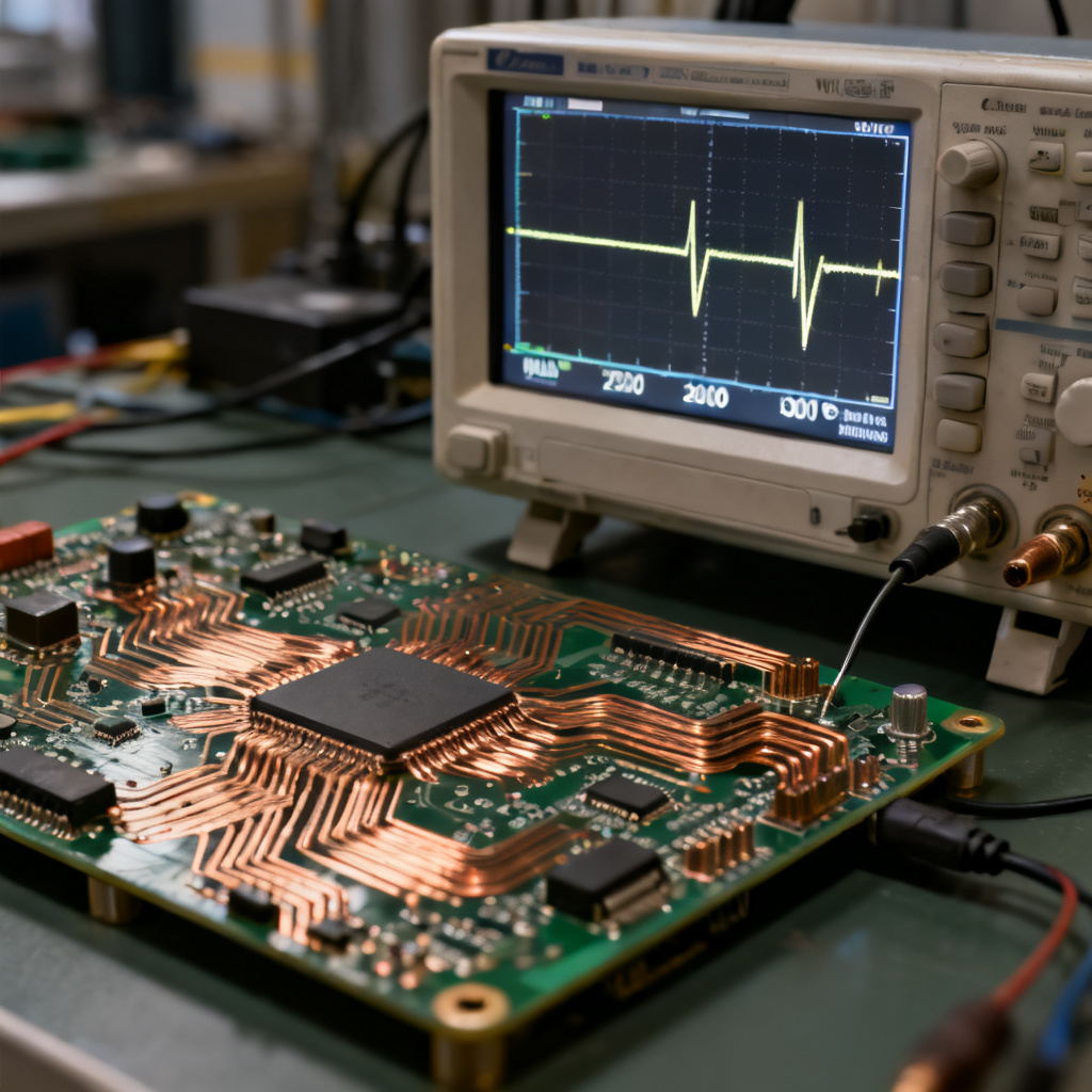
S-parameters: Use S-parameters (specifically S11 for return loss and S21 for insertion loss) to characterize your channel. A good rule: S11 < -15 dB up to the Nyquist frequency. Eye Diagram: The eye diagram is the ultimate SI metric. A wide-open eye (high vertical opening, low jitter) indicates a healthy channel. Closure indicates loss, crosstalk, or reflections.
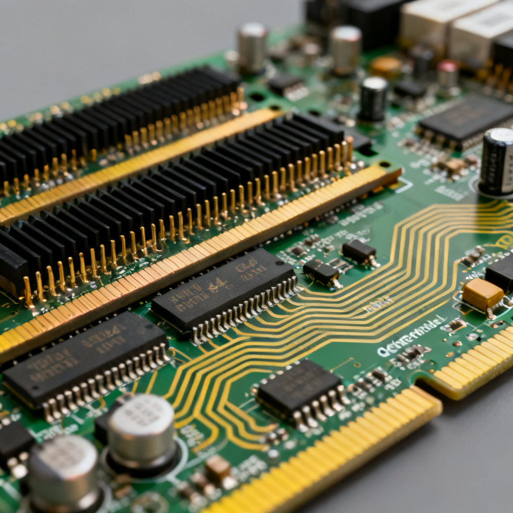
2. DDR Memory Interface Design – From DDR3 to DDR5
DDR Topologies and Routing in High-Speed Design
DDR (Double Data Rate) memory is the most common high-speed parallel bus in digital systems. Unlike serial links, DDR relies on strict timing relationships between data (DQ), data strobe (DQS), and clock (CK). T-Topology (DDR3, some DDR4): Used for 2-4 memory ranks. The address/command signals branch from a central point. Requires precise branch length matching. Fly-By Topology (DDR4, DDR5): The address/command signals daisy-chain from the controller to the last DRAM. This reduces reflections but introduces skew. All DDR5 designs must use fly-by. Data Group Routing: Each byte lane (DQ[0:7] + DQS + DM) must be routed as a group with tight length matching (typically ±10 mils for DDR4, ±5 mils for DDR5). Keep DQ traces on the same layer as their DQS.
Critical DDR Design Rules for High-Speed Design
- Length Matching is Not Just for Data: Address/command and clock signals must be length-matched to the longest data group. For DDR4, target ±50 mils between CK and DQS.
- VTT Termination: The address/command bus requires a termination voltage (VTT) at the end of the fly-by chain. Use a dedicated VTT regulator (e.g., TPS51200) and place it within 500 mils of the last DRAM.
- Power Delivery Network (PDN): DDR is sensitive to power supply noise. Use a 1.2V (DDR4) or 1.1V (DDR5) plane with low inductance. Place decoupling capacitors (100 nF + 10 µF) as close as possible to each DRAM VDD pin.
- Via Count: Minimize vias in DQ groups. Each via adds ~0.5 pF of capacitance and ~1 nH of inductance. For DDR5, limit to 2 vias per signal.
DDR Signal Integrity Specifics
Write Leveling (DDR4/DDR5): Compensates for CK-DQS skew in fly-by topology. Ensure your controller supports this. Read Training: The DRAM outputs data aligned to DQS. The controller must adjust its internal delay to capture the data correctly. This is handled by the memory controller, but your PCB layout must guarantee that the DQS and DQ traces are matched. DDR5 Special Requirements: DDR5 introduces Decision Feedback Equalization (DFE) on the data bus and uses a 14-bit CRC for error correction. Your PCB must maintain a channel loss of less than 7 dB at the data rate.
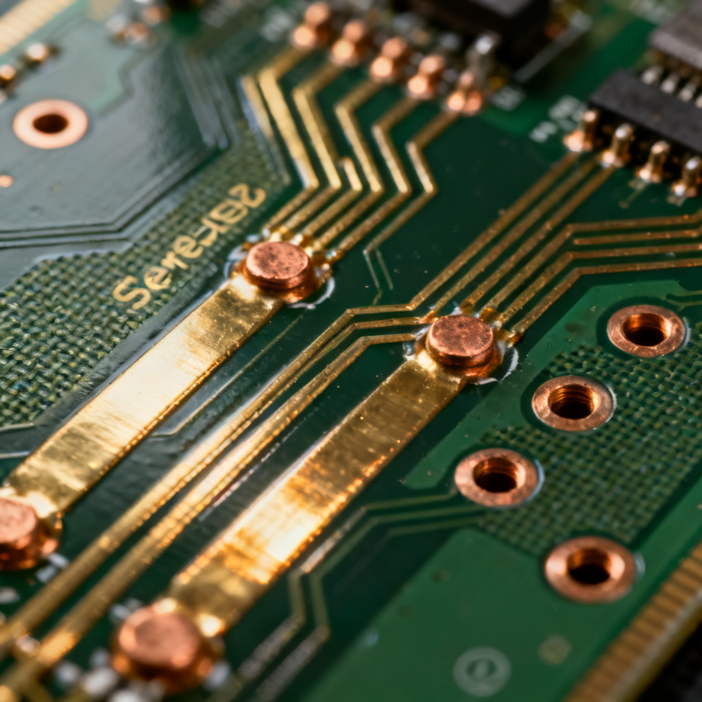
3. SerDes – High-Speed Serial Links (PCIe, USB, Ethernet)
The SerDes Channel in High-Speed Design
SerDes (Serializer/Deserializer) interfaces are the backbone of modern high-speed communication. Unlike DDR, SerDes is a serial, point-to-point link with embedded clocking. Examples: PCIe Gen 4/5, USB 3.2, 10 GbE, and HDMI 2.1. A typical SerDes channel consists of: TX Driver (a current-mode logic (CML) driver), PCB Trace (a differential pair with controlled impedance – 100 Ω differential), AC Coupling Capacitors (typically 100 nF placed near the TX or RX to block DC offset between chips), and RX Equalizer (a continuous-time linear equalizer (CTLE) and/or DFE to compensate for channel loss).
SerDes Layout Rules for High-Speed Design
- Differential Pair Routing: The two traces of a pair must be symmetrical (same length, same number of vias, same layer transitions). Intra-pair skew must be less than 5 mils for 10+ Gbps signals.
- Inter-Pair Spacing: Maintain 5x the dielectric height (H) between pairs to minimize crosstalk. For a standard 4-mil dielectric, space pairs at least 20 mils apart.
- Avoid 90° Corners: Use 45° chamfers or curved routing. A 90° corner creates an impedance bump and increases EMI.
- Reference Plane: Always route over a solid ground plane. Never allow the differential pair to cross a void or split. If a layer change is unavoidable, place a ground via within 50 mils of each signal via.
Key SerDes Parameters
Insertion Loss (IL): The total loss from TX to RX at the Nyquist frequency (half the data rate). For PCIe Gen 4 (16 GT/s), the maximum channel loss is 23 dB at 8 GHz. Return Loss (RL): Must be better than -10 dB across the operating band to avoid reflections. Jitter: Total jitter (TJ) is the sum of random jitter (RJ) and deterministic jitter (DJ). Deterministic jitter is caused by ISI (inter-symbol interference) and crosstalk. Common Mode Rejection: Ensure your differential pair is tightly coupled (edge-to-edge spacing = 1x trace width) to reject common-mode noise.
SerDes Equalization Techniques
Pre-emphasis / De-emphasis (TX): Boosts the high-frequency content of the signal to pre-compensate for channel loss. CTLE (RX): A high-pass filter that attenuates low frequencies and amplifies high frequencies. DFE (RX): A digital feedback filter that cancels post-cursor ISI. Essential for PCIe Gen 4 and above.
Common SerDes Pitfalls
Stubs from AC Coupling Caps: Place capacitors on the same layer as the trace. If you must use pads, ensure the pad size is no larger than the trace width to minimize capacitance. Connector Selection: Use high-speed connectors (e.g., Samtec, Molex) rated for your data rate. Connector insertion loss and crosstalk are often the bottleneck. Voltage Regulator Noise: SerDes PLLs (Phase-Locked Loops) are extremely sensitive to power supply ripple. Use LDOs with >60 dB PSRR at the SerDes frequency.
4. Stack-Up Design for High-Speed Signals
Your PCB stack-up is the single most important factor for High-Speed Design – Signal Integrity, DDR, SerDes performance.
Recommended 8-Layer Stack-Up for Mixed High-Speed Designs
| Layer | Signal Type | Notes for High-Speed Design |
|---|---|---|
| 1 | Top | Microstrip for SerDes, DDR, or components |
| 2 | Ground | Continuous plane, no splits |
| 3 | Inner Signal 1 | Stripline for DDR or slower buses |
| 4 | Power | Dedicated plane for VDD (e.g., 1.2V, 3.3V) |
| 5 | Ground | Continuous plane |
| 6 | Inner Signal 2 | Stripline for SerDes (preferred) |
| 7 | Ground | Continuous plane |
| 8 | Bottom | Microstrip for low-speed or additional SerDes |
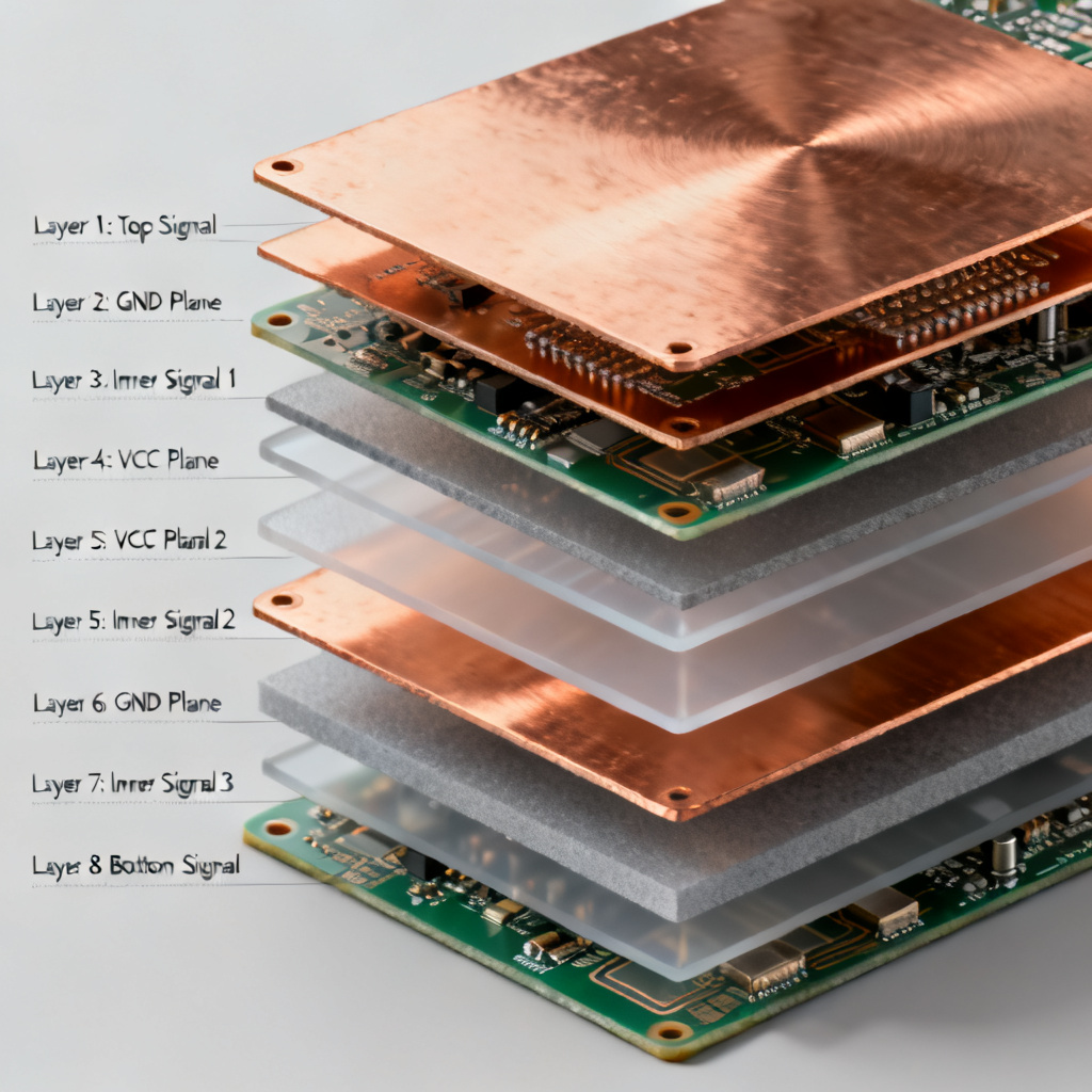
Key Stack-Up Rules
Dielectric Material: For 10+ Gbps SerDes, use low-loss materials (e.g., Megtron 6, Isola 370HR). FR-4 is acceptable up to ~3 Gbps. Core vs. Prepreg: Use core materials for impedance control. Prepreg thickness can vary during lamination. Symmetry: The stack-up must be symmetrical about the center to prevent warpage.
5. Simulation and Verification
Pre-Layout Simulation
IBIS Models: Use IBIS (I/O Buffer Information Specification) models for drivers and receivers. Simulate critical nets (clocks, DDR DQS, SerDes lanes) with a tool like HyperLynx or ADS. Timing Analysis: Verify setup and hold margins for DDR. Use a spreadsheet or dedicated tool to calculate flight time and skew.
Post-Layout Verification
3D EM Simulation: For critical SerDes channels, extract S-parameters using a 3D field solver (e.g., HFSS, CST). Compare to the channel budget. Time Domain Reflectometry (TDR): Measure impedance of fabricated boards. A deviation of >10% from target is a failure. Eye Diagram Testing: Use a real-time oscilloscope to capture eye diagrams at the receiver. For DDR4, a vertical eye opening of >200 mV is typical.
Conclusion: Bringing It All Together in High-Speed Design
High-speed design is not a checklist; it is a system-level discipline. High-Speed Design – Signal Integrity, DDR, SerDes provides the fundamental principles. DDR design adds the complexity of parallel buses, timing, and power delivery. SerDes design introduces equalization, channel budgets, and connector effects. At [Your Company Name], we manufacture PCBs that meet the most demanding high-speed requirements. Our engineering team reviews your stack-up, impedance, and routing before fabrication. We offer: controlled impedance testing (TDR) on every panel, back-drilling for through-hole vias, low-loss laminate options, and DFM feedback for high-speed rules. Ready to build your next high-speed design? Upload your Gerber files or contact our engineering team for a free design review.
Frequently Asked Questions about High-Speed Design – Signal Integrity, DDR, SerDes
What is the most critical aspect of High-Speed Design – Signal Integrity, DDR, SerDes?
How does DDR design differ from SerDes design in high-speed PCB layout?
What materials are recommended for High-Speed Design – Signal Integrity, DDR, SerDes?
Why Choose Us for Your High-Speed Design PCB Manufacturing?
We specialize in High-Speed Design – Signal Integrity, DDR, SerDes PCB fabrication. Unlike generic manufacturers, we offer controlled impedance testing (TDR) on every panel, back-drilling for via stubs, and low-loss laminate options. Our engineering team provides DFM feedback specific to high-speed rules, ensuring your design achieves first-pass success. We maintain strict quality control for impedance tolerance (±5%) and insertion loss verification, giving you confidence in your high-speed digital design.
Glossary of Key Terms in High-Speed Design – Signal Integrity, DDR, SerDes
- Signal Integrity (SI): The quality of an electrical signal in a high-speed design, ensuring minimal distortion.
- DDR: Double Data Rate memory interface, a parallel bus requiring precise timing and length matching.
- SerDes: Serializer/Deserializer, a high-speed serial link with embedded clocking.
- Impedance Discontinuity: A change in characteristic impedance causing reflections in high-speed design.
- Eye Diagram: A graphical representation of signal quality, showing voltage margin and jitter.
- Insertion Loss (S21): The loss of signal power as it travels through a channel.
- Return Loss (S11): The amount of signal reflected back due to impedance mismatch.
- Fly-By Topology: A daisy-chain routing method for DDR address/command signals.
- CTLE: Continuous-Time Linear Equalizer, used in SerDes receivers to compensate for channel loss.
- DFE: Decision Feedback Equalization, a digital filter for post-cursor ISI cancellation.