Design for Test Test Point Placement ICT Access
In B2B PCB manufacturing, Design for Test Test Point Placement ICT Access is the cornerstone of reliable production. This guide consolidates top industry knowledge to help you master DFT for high-yield, cost-efficient boards.
DFT Fundamentals for Test Point Placement and ICT Access
Design for Test – Test Point Placement, ICT Access is a systematic engineering approach that integrates testability into PCB layout. Its primary goal is to ensure every solder joint and component is correctly placed and soldered, minimizing false failures and maximizing fault coverage.

What is Design for Test (DFT)?
DFT is a set of design rules that make a PCB easier to test after assembly. In the context of PCB manufacturing, Design for Test – Test Point Placement, ICT Access directly impacts production yield, test cycle time, and overall product quality.
The Role of Test Points in ICT
Test points are dedicated pads or vias on a PCB that allow test probes to make electrical contact with the board’s internal nets. Without well-placed test points, ICT cannot access critical nodes, leading to incomplete testing and potential field failures. Key functions include enabling electrical continuity checks, allowing measurement of component values, facilitating in-system programming, and supporting boundary-scan testing.
ICT vs. Flying Probe Testing: Choosing the Right Approach
While ICT uses a bed-of-nails fixture for high-volume production, flying probe testers use moving probes for low-volume or prototype runs. For high-volume orders, prioritize ICT-compatible test point placement. For prototypes, design with flying probe in mind but ensure all critical nets have test points.
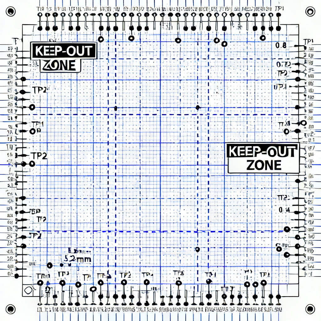
Test Point Placement: The Golden Rules for ICT Access
Based on industry best practices and IPC-9850 standards, the following rules ensure reliable Design for Test – Test Point Placement, ICT Access:
Placement Rules for ICT Access
Rule 1: Use Dedicated Test Pads, Not Component Leads. Never rely on component leads as test points. Instead, add dedicated test pads on the copper layer.
Rule 2: Minimum Test Point Size. For ICT, 0.035 inch diameter is the minimum; 0.040 inch is preferred. For flying probe, 0.020 inch is acceptable.
Rule 3: Test Point Spacing. Center-to-center spacing should be minimum 0.100 inch for ICT fixtures. For flying probe, 0.050 inch is possible.
Rule 4: Keep-Out Zones. Maintain a 0.100 inch keep-out zone around each test point. No components or vias should be within this radius.
Rule 5: Test Point Shape and Orientation. Use round or square pads with no sharp corners. For ICT, orient all test points in a consistent grid pattern.
Rule 6: Test Point Accessibility. Ensure test points are on the bottom side for single-sided ICT. Avoid placing test points under components.
Best Practices for High-Density Boards
In modern designs with fine-pitch components, use via-in-pad with care, leverage boundary-scan, add test points on inner layers via microvias, and cluster test points to reduce fixture travel time.
Common Mistakes to Avoid
Avoid placing test points on power or ground planes without isolation, using solder mask over test points, or ignoring component height that can block probes.
ICT Access: Designing for Fixture Compatibility
Understanding ICT fixture design is critical for Design for Test – Test Point Placement, ICT Access. An ICT fixture uses spring-loaded probe pins aligned with test points. For your PCB to be ICT-ready, all test points must be on the same side and align with a standard grid.

Test Point Coverage Requirements
Industry standards recommend 95% to 100% node coverage for ICT. Every net except power and ground should have at least one test point. For critical nets, add redundant test points.
Test Point Assignment for Specific Components
For resistors and capacitors, place test points on both ends. For ICs, use JTAG or boundary-scan. For connectors, add test points nearby if not directly accessible. Use a single test point for each power rail and ground plane.
Dealing with High-Speed and Analog Signals
For high-speed signals, avoid adding test points directly on the trace to prevent impedance discontinuities. For analog signals, place test points far from noisy digital traces.
Advanced DFT Strategies for Complex Boards
Combining ICT with other test methods like AOI, X-Ray, and functional test maximizes fault coverage. For multi-layer and HDI boards, use microvias for test points on inner layers and design test points on both sides if necessary.

DFM (Design for Manufacturability) Integration
Test point placement must not conflict with DFM rules. Keep test points away from solder mask openings for SMD pads and avoid placing them near edge connectors or mounting holes.
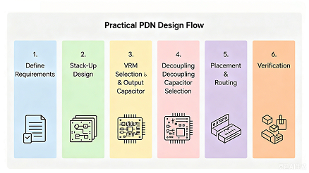
Practical Implementation: Step-by-Step Guide
Step 1: Define test strategy early during schematic design. Step 2: Allocate space for test points. Step 3: Place test points in layout using a 0.100 inch grid for ICT. Step 4: Generate test point report. Step 5: Verify with manufacturer.
Comparison: Our DFT Services vs. Standard Approaches
| Feature | Standard Approach | Our Design for Test – Test Point Placement, ICT Access |
|---|---|---|
| Test Point Coverage | 80-90% | 95-100% |
| Fixture Compatibility | Manual adjustment | Pre-verified grid alignment |
| High-Speed Signal Handling | Impedance risk | Stub-free test points |
| Cost Efficiency | Higher rework cost | Reduced fixture complexity |
Key Terminology in Design for Test – Test Point Placement, ICT Access
ICT (In-Circuit Test): A testing method using a bed-of-nails fixture to verify component placement and soldering. Flying Probe: A flexible testing method using moving probes. Boundary-Scan (JTAG): A technique for testing interconnects on complex digital circuits without physical test points. Node Coverage: The percentage of nets accessible via test points.
FAQ: Design for Test – Test Point Placement, ICT Access
Can I use vias as test points for ICT access?
Yes, but only if they are tented on the opposite side and have adequate pad size. Dedicated test pads are more reliable for Design for Test – Test Point Placement, ICT Access.
What is the minimum test point size for 0.100 inch pitch ICT?
0.035 inch (0.9 mm) is the minimum; 0.040 inch (1.0 mm) is recommended for reliable test point placement.
How many test points do I need for typical PCB ICT access?
Aim for 1 test point per net plus 1 for each power rail. A 100-net board might need 120 test points for proper Design for Test – Test Point Placement, ICT Access.
What if I cannot fit all test points on my PCB?
Use boundary-scan (JTAG) for digital nets or move test points to inner layers with microvias to maintain ICT access coverage.
How does test point placement affect manufacturing cost?
Proper placement reduces fixture complexity and probe wear, lowering overall test cost. Poor placement can double fixture costs in Design for Test – Test Point Placement, ICT Access.