Ultimate PCB Design Guide: From Schematic to Manufacturing
The Ultimate PCB Design Guide From Schematic to Manufacturing is your definitive resource for mastering printed circuit board development. This comprehensive PCB design guide covers every critical phase, from initial circuit concept to reliable, manufacturable product, ensuring engineers and procurement professionals achieve success in B2B PCB production and export.

This guide synthesizes industry best practices from leading engineering authorities, providing a complete roadmap for the transition from a logical schematic to a physical, manufacturable PCB.
Part 1: The Foundation – Schematic Capture and Circuit Design
The schematic is the logical heart of your PCB design. It defines the electrical connectivity between components but does not dictate their physical layout. A well-structured schematic is the first step toward a successful PCB design.
1.1 Symbol Creation and Library Management
Adhere to industry-standard symbols (e.g., IEEE/ANSI) for components like resistors, capacitors, ICs, and connectors. Every component should have a unique reference designator (e.g., R1, C2, U3) and accurate parameters (value, tolerance, voltage rating, footprint). For ICs, ensure power and ground pins are correctly connected in the symbol, even if not visible on the schematic sheet.
1.2 Hierarchical Design and Net Labeling
For complex circuits, break the schematic into hierarchical sheets to improve readability and allow reuse of functional blocks. Use explicit net labels (e.g., VCC_5V, I2C_SCL, RESET_N) for critical signals, and distinguish between global nets (power, ground, reset) and local nets confined to a single sheet.
1.3 Critical Design Considerations at the Schematic Stage
Every IC should have at least one 0.1µF ceramic decoupling capacitor placed as close as possible to its power pin. Document the power tree including input voltage, regulators, and voltage rails for each subsystem. Identify high-speed signals (clocks, data buses, RF) and note impedance requirements (e.g., 50Ω single-ended, 100Ω differential) as design constraints for layout.
Part 2: The PCB Stack-Up – Engineering Your Layer Structure
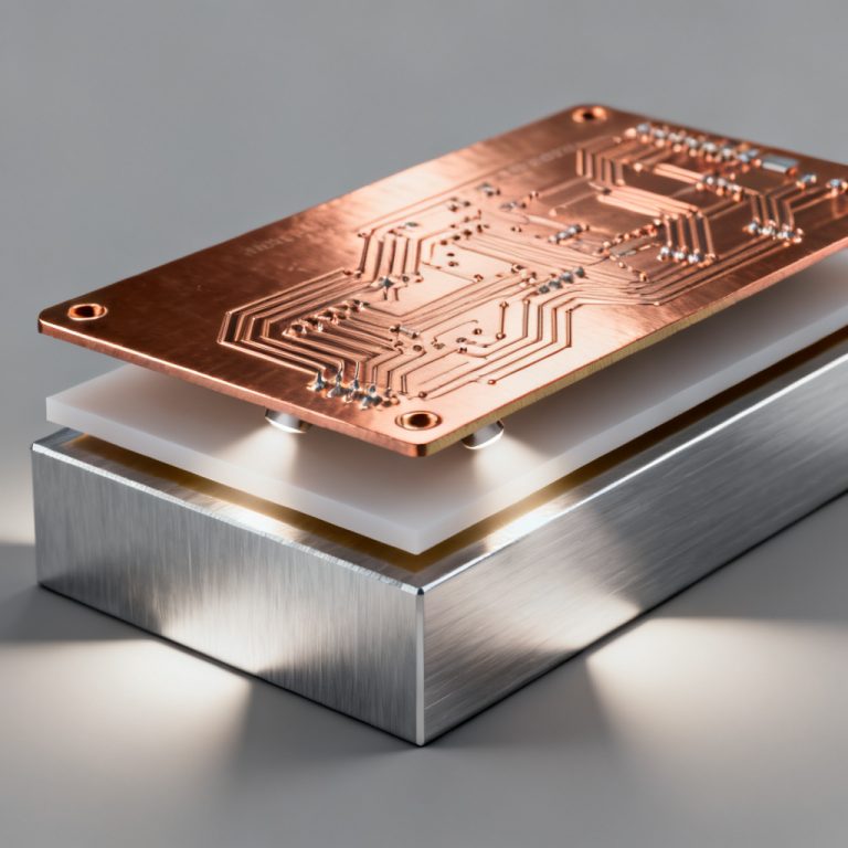
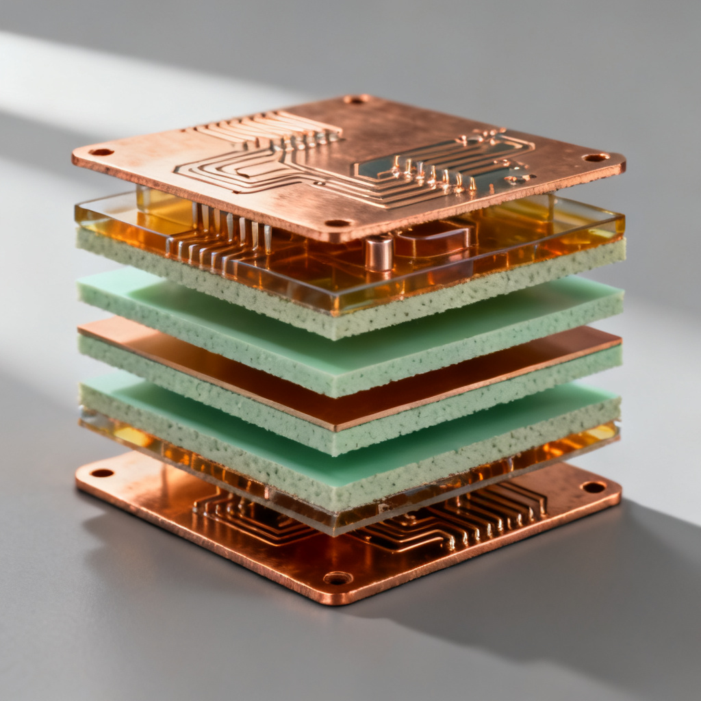
The stack-up defines the number of copper layers, their thickness, insulating materials, and order. This decision directly impacts signal integrity, power delivery, EMI performance, and manufacturing cost in your PCB design.
2.1 How Many Layers Do You Need?
| Layer Count | PCB Design Application | Key Benefits |
|---|---|---|
| 2-Layer | Low-speed, simple analog or basic microcontroller projects | Lowest cost, suitable for simple circuits |
| 4-Layer | Standard modern designs (microcontrollers, mixed-signal) | Excellent signal integrity and EMI reduction |
| 6+ Layer | High-speed digital (DDR, serdes), RF, complex mixed-signal | Dedicated power islands, multiple ground planes, controlled impedance |
2.2 Material Selection and Prepreg/Core Thickness
FR-4 is the most common and cost-effective material for general-purpose PCB designs below 1 GHz. High-Tg FR-4 (170°C+) is recommended for lead-free soldering and thermally demanding applications. For RF above 1 GHz or low-loss requirements, use Rogers, Teflon (PTFE), or Isola materials with stable dielectric constant (Dk) and low dissipation factor (Df).
2.3 Controlled Impedance Design
Most manufacturers can achieve ±10% impedance tolerance. Specify this requirement explicitly in fabrication notes for critical designs. Use microstrip for outer layers with a reference plane below, or stripline for inner layers between two reference planes for superior shielding. Use a field solver tool to calculate impedance and provide target impedance, trace width, and stack-up details to your manufacturer.
Part 3: Component Placement – The Art of Physical Organization
Placement is the most critical step in PCB design layout. It determines routing feasibility, thermal performance, and signal integrity. A poor placement cannot be fixed by clever routing.
3.1 Functional Block Placement
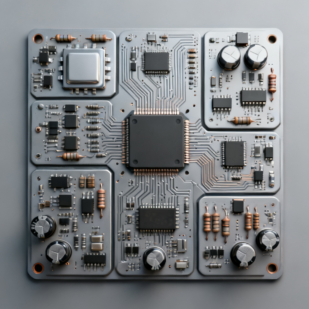
Group components belonging to the same functional block in close physical proximity to minimize trace lengths and reduce crosstalk. Physically partition the board into analog, digital, and power sections. Place I/O connectors, power jacks, and headers near the board edge.
3.2 Critical Component Positioning
Place crystal oscillators and high-speed clocks as close as possible to the target IC. Position decoupling capacitors within 2-3mm of the IC’s power pin. Place voltage regulators, inductors, and large capacitors near the point of load. Keep sensitive components like op-amps and ADCs away from noisy digital traces and switching power supplies.
3.3 Mechanical and Thermal Considerations
Check the 3D model to ensure no component protrudes into an enclosure. Identify high-power components and ensure sufficient copper area for heat sinking. Add thermal vias under QFN packages or exposed pads. For automated assembly, orient all similar components in the same direction.
Part 4: Routing – Connecting the Dots with Precision
Routing is the process of laying copper traces to connect all pins according to the netlist. This is where signal integrity, power integrity, and manufacturability are realized in your PCB design.
4.1 General Routing Best Practices
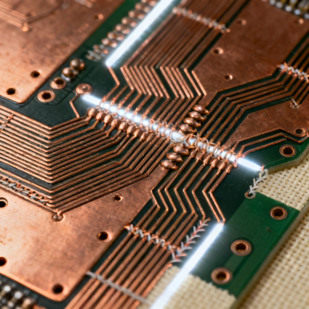
Route high-speed signals, differential pairs, and sensitive analog traces before anything else. Minimize via count to reduce inductance and capacitance. Use 45-degree chamfers or curved traces for all corners. Keep traces short and direct for optimal signal integrity.
4.2 Power and Ground Routing
Use dedicated power and ground planes on 4-layer or more boards. For analog and mixed-signal circuits, use a single point of connection for all ground returns (star-ground) to prevent ground loops. On power planes, create separate islands for different voltage rails and avoid routing high-speed signals across splits in the ground plane.
4.3 High-Speed Routing Techniques
For differential pairs like USB, HDMI, and Ethernet, route traces as tightly coupled pairs with constant spacing and equal length. Match trace lengths for parallel buses within specified tolerance. Avoid stubs on signal traces. For extremely sensitive analog signals, route grounded guard traces on both sides of the signal trace.
4.4 Via Usage and Types
Through-hole vias are suitable for low-to-moderate speed designs. Blind and buried vias are used in high-density designs (HDI) for space-critical applications. Use via stitching to improve EMI shielding and reduce ground impedance by placing multiple vias connecting ground planes around the board perimeter.
Part 5: Design for Manufacturing (DFM) – Ensuring Your Board Can Be Built
DFM is the process of designing your PCB design so that it can be manufactured reliably, cost-effectively, and without yield loss. Ignoring DFM leads to delays, rework, and increased costs.
5.1 Minimum Trace Width and Spacing
Most PCB fabricators can reliably produce 6/6 mil (0.15mm) trace/space. For high-volume or cost-sensitive designs, use 8/8 mil or larger. For high-current paths, calculate required trace width based on copper weight and allowable temperature rise using IPC-2221 calculators.
5.2 Annular Ring and Pad Design
The copper ring around a drilled hole must have a minimum width of 6-8 mils for through-hole components. Use tented vias for vias that should not be soldered. Add teardrops to pads and vias where traces enter at an angle to strengthen the connection.
5.3 Solder Mask and Silkscreen
The solder mask opening should be slightly larger than the copper pad (2-3 mils per side). Avoid creating narrow strips of solder mask between pads or traces (less than 4 mils). Keep silkscreen text outside of solder pads and vias, using a font size of at least 40 mils.
5.4 Panelization and Breakaway Tabs
For small boards, consider panelizing multiple copies in a single array to improve manufacturing efficiency. Use V-scoring for rectangular boards with straight edges, and tab routing for irregularly shaped boards. Include at least two non-plated tooling holes (3mm diameter) on the panel.
5.5 Fabrication and Assembly Documentation
Generate a complete Gerber file set including top and bottom copper, solder mask, silkscreen, drill file, and outline/board edge file. Include a readme file with board name, revision, date, stack-up details, and impedance requirements. Create a structured BOM with manufacturer part numbers, quantities, and reference designators.
Part 6: Verification and Testing – Catching Errors Before Production
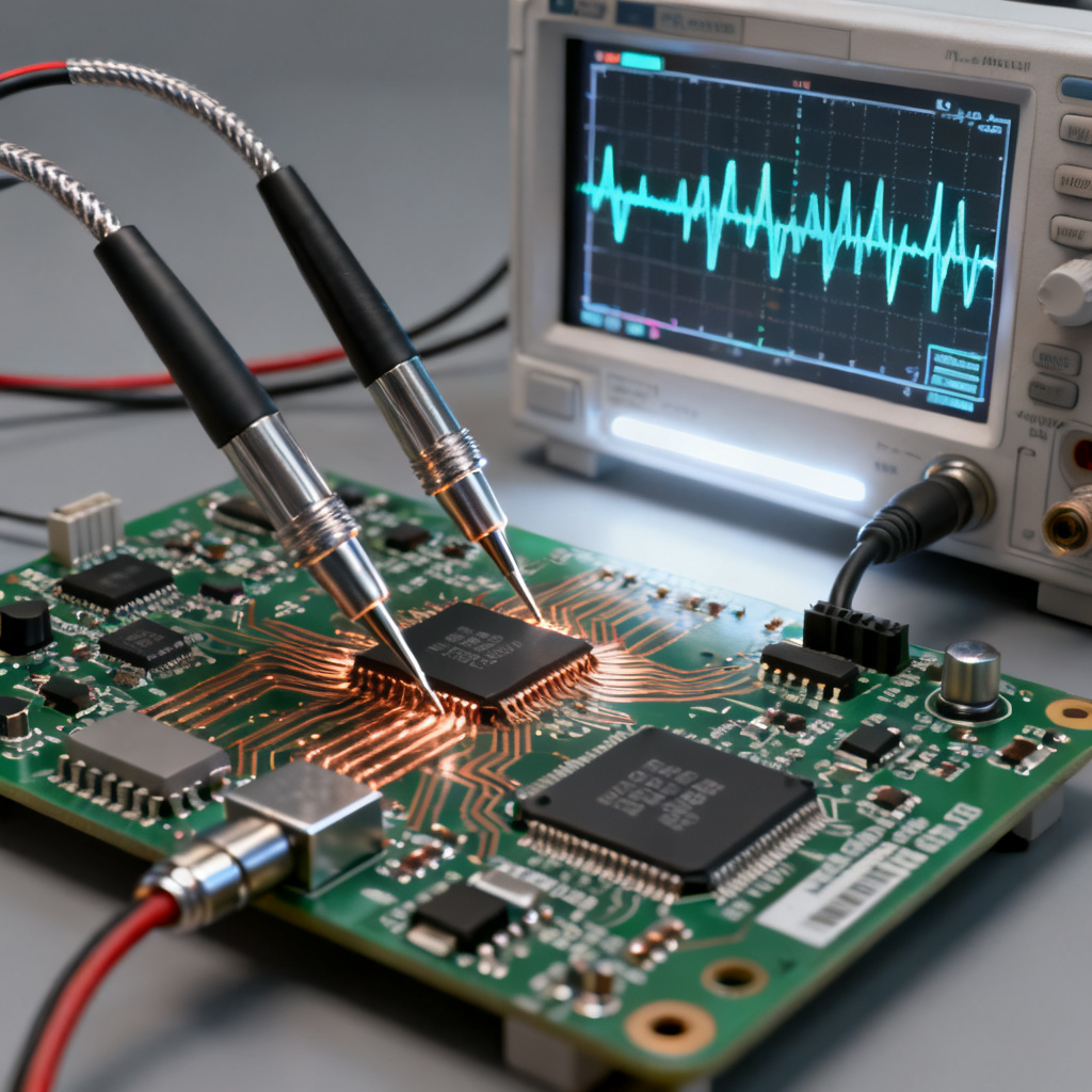
Before sending your PCB design to fabrication, rigorous verification is essential.
6.1 Design Rule Check (DRC)
Run DRC after every major routing step to check for clearance violations, unconnected nets, short circuits, and minimum width/spacing violations. Set specific rules for different net classes.
6.2 Electrical Rule Check (ERC)
Check for unconnected input pins, multiple drivers on a single net, and floating outputs to prevent logic-level conflicts and undefined states.
6.3 Signal Integrity (SI) and Power Integrity (PI) Simulation
For high-speed designs with clock frequencies above 50 MHz, run SI simulations to check for reflections, overshoot, and ringing. Simulate power delivery network impedance to ensure it is below target values.
6.4 Final Review Checklist
Verify that the netlist matches the schematic exactly. Check that footprint dimensions match component data sheets. Review the fabrication drawing for correct board outline and dimension tolerances. Ensure pads connected to large copper pours have thermal relief spokes.
Conclusion: From Design to Delivery
The journey from schematic to manufactured PCB is a disciplined process that rewards careful planning and attention to detail. By mastering the principles outlined in this PCB design guide, you can consistently produce boards that function correctly, are easy to assemble, and arrive on time and within budget. Key takeaways include starting with a clean schematic, planning your stack-up carefully, placing components thoughtfully, routing with discipline, designing for manufacturing from day one, and verifying everything before release.
Frequently Asked Questions (FAQ)
What is the most important step in PCB design?
The most important step in any PCB design is schematic capture, as it defines the logical connectivity and sets the foundation for all subsequent phases of the design process.
How many layers should my PCB design have?
The number of layers in your PCB design depends on complexity: 2-layer boards suit simple circuits, 4-layer boards are standard for most modern designs, and 6+ layers are required for high-speed digital or RF applications.
What is controlled impedance in PCB design?
Controlled impedance in PCB design refers to maintaining a consistent characteristic impedance for traces, typically 50Ω single-ended or 100Ω differential, to ensure signal integrity in high-speed circuits.
Why is DFM important in PCB design?
DFM (Design for Manufacturing) is critical in PCB design to ensure the board can be built reliably and cost-effectively, avoiding delays, rework, and increased production costs.