PCB Materials Science: Substrates, Copper, Prepreg & Finish Guide
Mastering PCB materials science substrates copper prepreg finish selection is the foundation of reliable electronics. The choice of these materials directly impacts electrical performance, thermal management, mechanical stability, and long-term reliability.
1. Substrates – The Core of PCB Materials Science
1.1 What Are PCB Substrates?
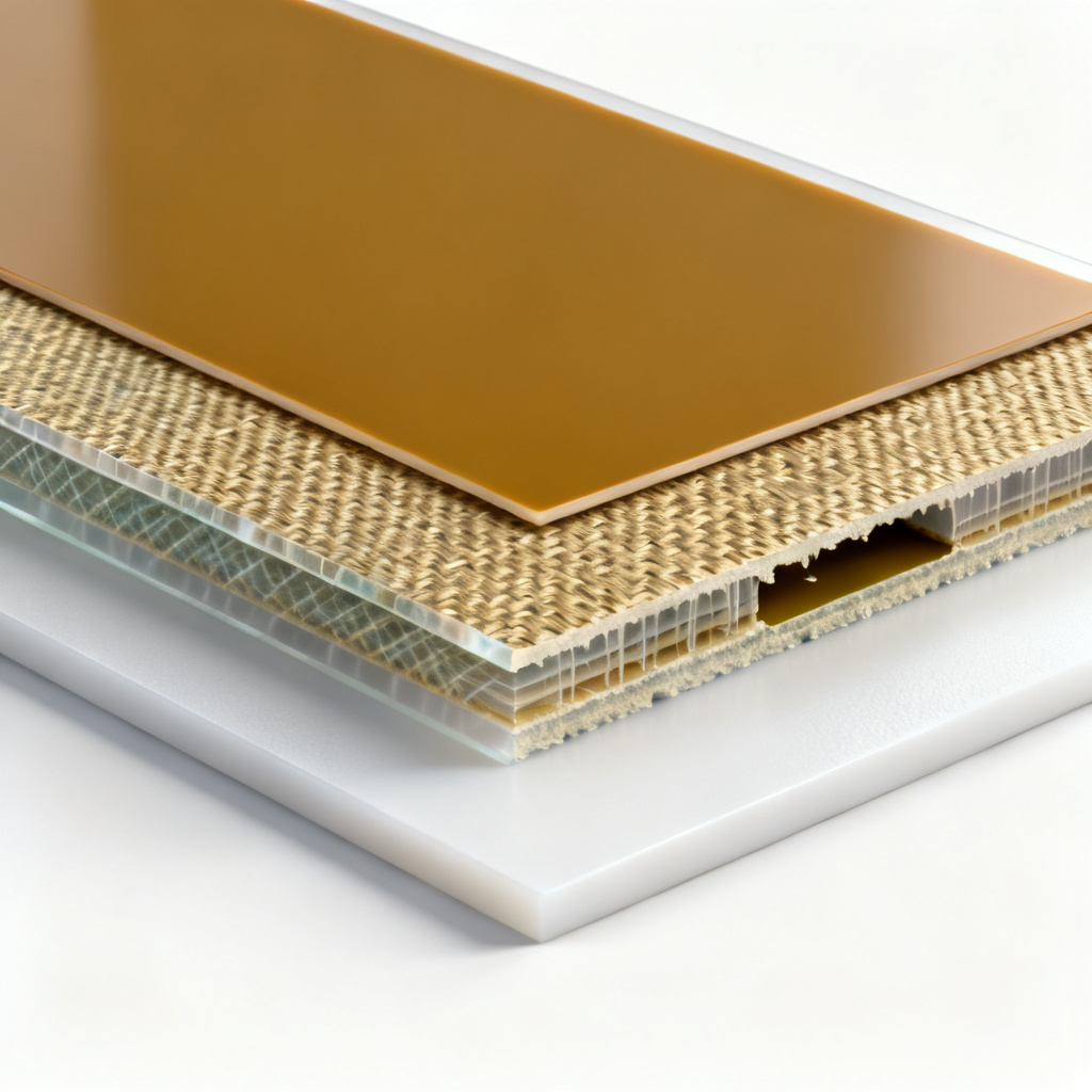
The substrate is the base insulating material that provides mechanical support and electrical isolation for copper traces. It is typically a composite of a reinforcing fabric (e.g., woven glass fiber) and a resin system (e.g., epoxy, polyimide, PTFE). The substrate determines the dielectric constant (Dk), dissipation factor (Df), thermal conductivity, and coefficient of thermal expansion (CTE) in PCB materials science.
1.2 Common Substrate Types
| Substrate Type | Key PCB Materials Science Properties | Typical Applications |
|---|---|---|
| FR-4 | Dk ~4.5, Df ~0.02, Tg 130–180°C | General digital/analog, consumer electronics |
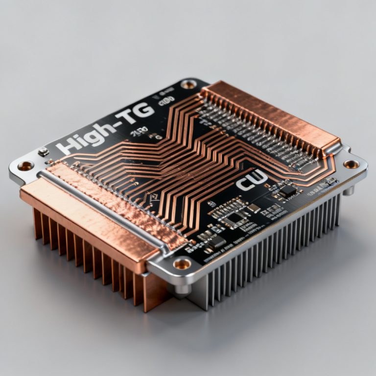
| High-Tg FR-4 | Tg 170–180°C, improved thermal reliability | Lead-free soldering, automotive |
| Polyimide | Tg >250°C, Dk ~3.5, Df ~0.01 | Aerospace, military, high-temp environments |
| PTFE (Teflon) | Dk ~2.1–2.5, Df ~0.0002–0.001 | RF/microwave, antennas, high-speed digital |
| Rogers | Dk 2.2–10.2, Df 0.0009–0.0025 | 5G infrastructure, automotive radar |
| CEM-1/CEM-3 | Lower cost, moderate electrical performance | Low-cost consumer, single-sided boards |
FR-4 remains the most common substrate in PCB materials science, but for high-frequency designs, PTFE or Rogers materials are preferred due to their lower Dk and Df values.
1.3 Key Substrate Parameters in PCB Materials Science
Evaluating substrates in PCB materials science requires understanding these parameters: Glass Transition Temperature (Tg) – the temperature at which resin transitions from rigid to rubbery; Decomposition Temperature (Td) – temperature at which 5% mass loss occurs; Dielectric Constant (Dk) – affects signal propagation speed; Dissipation Factor (Df) – indicates signal loss; Coefficient of Thermal Expansion (CTE) – matching CTE with copper prevents delamination; Moisture Absorption – degrades electrical properties and can cause CAF growth. Higher Tg (≥170°C) is essential for lead-free soldering, while lower Df (<0.01) is critical for high-speed signals in PCB materials science.
2. Copper – The Conductive Backbone in PCB Materials Science
2.1 Types of Copper Foils
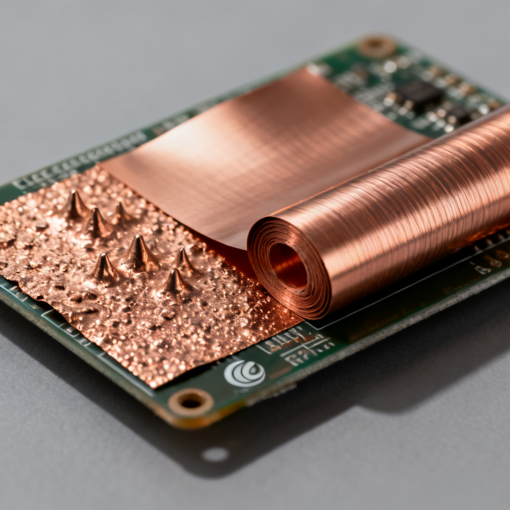
Copper is the primary conductive material in PCB materials science, available as electrodeposited (ED) or rolled-annealed (RA) foil. Electrodeposited (ED) copper is low cost with high strength but has higher surface roughness, increasing signal loss at high frequencies. Rolled-annealed (RA) copper offers excellent ductility and low surface roughness, making it ideal for flexible circuits and high-frequency RF boards in PCB materials science.
2.2 Copper Weight and Thickness
Copper thickness in PCB materials science is measured in ounces per square foot: 0.5 oz (17.5 µm) for fine-pitch traces, 1 oz (35 µm) for standard boards, 2 oz (70 µm) for high-current circuits, and 3 oz+ for heavy copper designs. Thicker copper requires wider trace widths to maintain controlled impedance, a key consideration in PCB materials science.
2.3 Copper Surface Treatments for Adhesion
To ensure strong bonding between copper and prepreg, surfaces are chemically roughened using brown oxide, black oxide, or alternative organic treatments like CZ-8100. These treatments enhance adhesion but must be carefully controlled to avoid brittleness, especially in fine-line designs within PCB materials science.
2.4 Copper in High-Frequency Designs
At frequencies above 1 GHz, the skin effect forces current near the conductor surface, making surface roughness critical. For high-frequency PCB materials science, RA copper or low-profile ED copper (e.g., RTF) is recommended to minimize signal loss. Low-roughness copper (<1.5 µm Rz) is essential for 5G and millimeter-wave applications.
3. Prepreg – The Bonding Layer in PCB Materials Science
3.1 What is Prepreg?
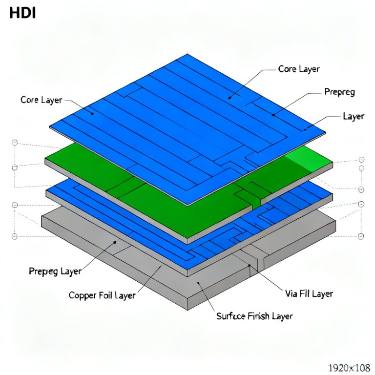
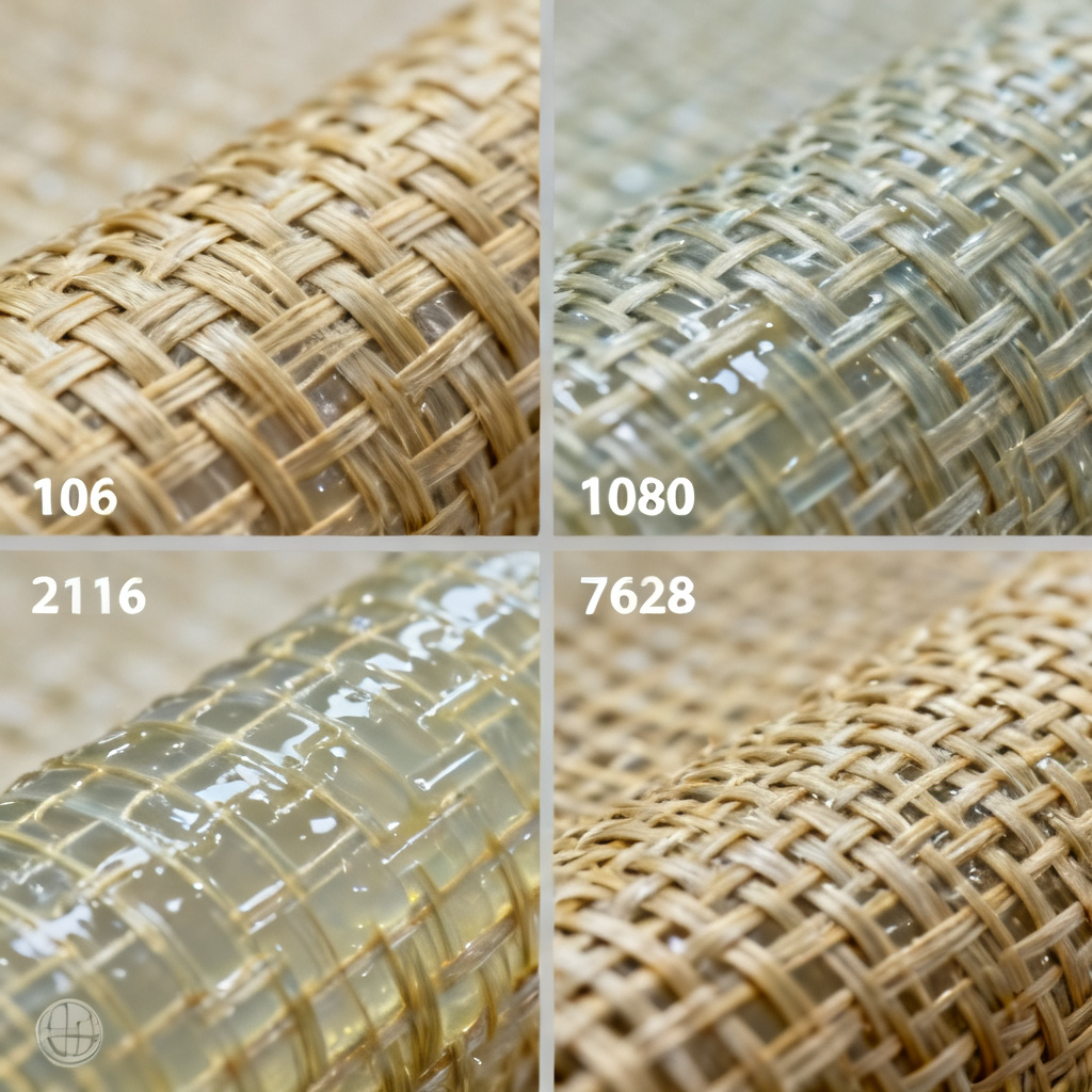
Prepreg (pre-impregnated) is a sheet of glass fabric pre-coated with partially cured resin (B-stage), used as the bonding layer between copper foils and cores in multilayer PCBs. During lamination, heat and pressure fully cure the resin, creating a monolithic structure critical to PCB materials science.
3.2 Prepreg Resin Systems
Common prepreg resin systems in PCB materials science include standard epoxy (FR-4 type, Dk ~4.2–4.5, Df ~0.02), high-Tg epoxy for lead-free soldering, low-loss prepreg (e.g., Rogers 4450F, Df <0.01) for high-speed digital, and PTFE prepreg (e.g., Rogers 2929) for RF/microwave multilayers.
3.3 Prepreg Glass Styles
| Glass Style | Thickness (after cure) | Resin Content | Typical Use in PCB Materials Science |
|---|---|---|---|
| 106 | ~2.0 mil (0.05 mm) | High (70%) | Thin dielectric layers, HDI |
| 1080 | ~2.7 mil (0.07 mm) | High (65%) | Controlled impedance, fine pitch |
| 2116 | ~4.5 mil (0.11 mm) | Medium (55%) | Standard multilayer |
| 7628 | ~7.0 mil (0.18 mm) | Low (45%) | Thick layers, high mechanical strength |
Thinner glass styles (106, 1080) have higher resin content, reducing Dk and improving impedance control, while thicker styles (7628) provide better rigidity in PCB materials science.
3.4 Prepreg Selection Criteria
Selecting prepreg in PCB materials science requires matching Dk to cores for consistent impedance, choosing high-Tg prepreg for thermal reliability, using low-flow prepreg for cavity designs, and selecting high-resin prepreg (e.g., 106) to fill gaps in HDI designs.
3.5 Prepreg in Multilayer Stackups
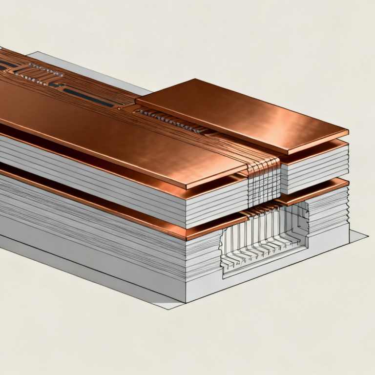
A typical 4-layer stackup using FR-4 in PCB materials science: Layer 1 copper foil, prepreg (e.g., 2116), core (1 oz copper on 0.5 mm FR-4), prepreg (e.g., 1080), core, prepreg (e.g., 2116), Layer 4 copper foil. For high-speed designs, cores offer tighter Dk/Df tolerances than prepreg.
4. Surface Finish – Protecting the Copper in PCB Materials Science
4.1 Why Surface Finish Matters
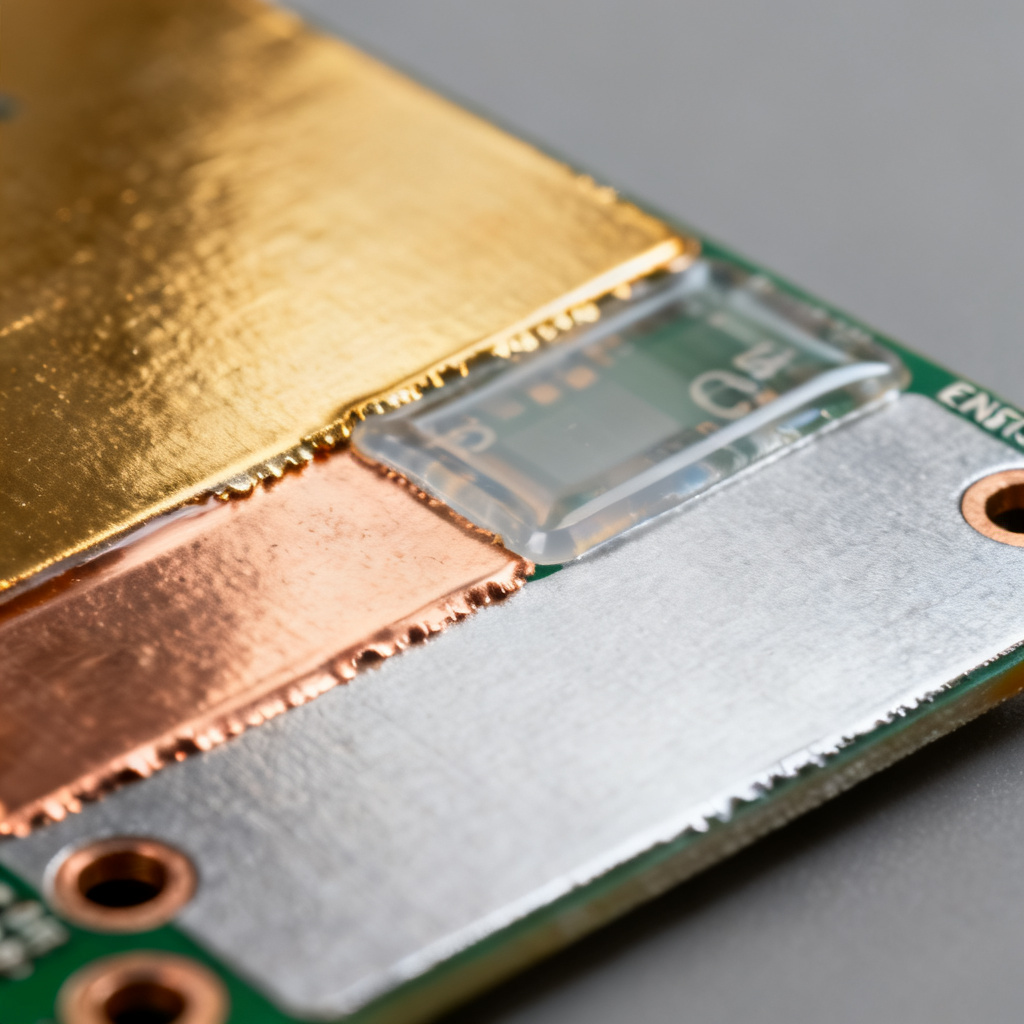
Copper oxidizes rapidly, forming a non-conductive layer. Surface finishes in PCB materials science provide corrosion resistance, solderability, and protect underlying copper from contamination.
4.2 Common Surface Finishes
| Surface Finish | Process | Key PCB Materials Science Features | Applications |
|---|---|---|---|
| HASL | Hot air solder leveling | Lowest cost, excellent solderability | General-purpose, cost-sensitive |
| Lead-Free HASL | SAC alloy | RoHS-compliant, good solderability | RoHS designs |
| ENIG | Electroless nickel + immersion gold | Excellent corrosion resistance, flat surface | HDI, BGA, fine-pitch |
| ENEPIG | Nickel + palladium + gold | Eliminates black pad, excellent wire bonding | Advanced packaging, high-reliability |
| OSP | Organic coating | Low cost, flat surface | Short-shelf-life, low-cost |
| Immersion Silver | Silver deposition | Excellent planar flatness, low loss | High-frequency RF |
| Immersion Tin | Tin deposition | Flat surface, good solderability | Press-fit connectors |
| Hard Gold | Electrolytic gold | Excellent wear resistance | Edge connectors, contacts |
ENIG is widely used in PCB materials science for fine-pitch BGA due to its flat surface, while immersion silver is preferred for high-frequency RF applications due to minimal signal loss.
4.3 Finish Selection Guide
For fine-pitch BGA (<0.5mm pitch), use ENIG or ENEPIG. For high-frequency RF (>1 GHz), use immersion silver or ENIG. For automotive, use ENEPIG or LF-HASL. For low-cost consumer, use OSP or HASL. For edge connectors, use hard gold. For press-fit connectors, use immersion tin. These selections optimize PCB materials science for specific applications.
4.4 Surface Finish and Signal Integrity
At high frequencies, surface finish impacts signal loss in PCB materials science. ENIG adds insertion loss (0.1–0.2 dB/inch at 10 GHz) due to nickel’s magnetic properties, while immersion silver offers the lowest loss among common finishes. OSP has minimal impact but requires careful handling to avoid oxidation.
5. Material Selection for Specific Applications in PCB Materials Science
High-speed digital (>1 Gbps): Use low-loss FR-4 (e.g., Isola 370HR) or Rogers 3000 series, low-profile ED or RA copper, low-loss prepreg (e.g., 4450F), and immersion silver or ENIG finish. RF/microwave (>1 GHz): Use Rogers 4000 series or PTFE laminates, RA copper, matching prepreg, and immersion silver finish. High-power (>100W): Use high-Tg FR-4 or metal-core with aluminum base, thick copper (2–4 oz), high-Tg prepreg with thermal conductivity 0.8–1.5 W/mK, and LF-HASL or ENIG finish. Flexible circuits (FPC): Use polyimide substrate, RA copper, adhesive-less bonding layers, and ENIG or immersion silver finish. These material choices are central to advanced PCB materials science.
6. Material Testing and Qualification in PCB Materials Science
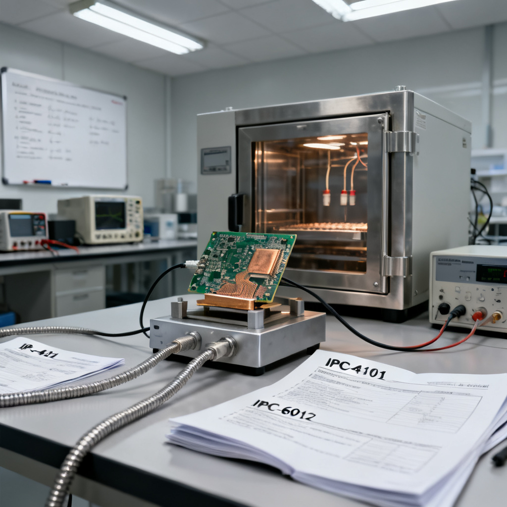
To ensure reliability, materials must be tested per IPC standards. IPC-4101 specifies base materials. IPC-6012 covers rigid PCB qualification. IPC-TM-650 defines test methods for thermal, electrical, and mechanical properties. CAF testing (IPC-TM-650 2.6.25) measures resistance to conductive anodic filament growth. Thermal cycling (IPC-9701) simulates soldering stress. Key tests include Tg/Td verification, peel strength (minimum 6 lb/in for 1 oz copper), and dielectric breakdown (>40 kV/mm for FR-4). These tests validate PCB materials science performance.
Frequently Asked Questions about PCB Materials Science
What is the most common substrate in PCB materials science?
FR-4 is the most common substrate in PCB materials science, offering a balance of cost, mechanical strength, and electrical performance for general-purpose applications.
How does copper type affect PCB materials science for high-frequency designs?
In PCB materials science, rolled-annealed (RA) copper or low-profile ED copper is recommended for high-frequency designs because lower surface roughness reduces skin effect losses, critical for signals above 1 GHz.
What surface finish is best for fine-pitch BGA in PCB materials science?
ENIG or ENEPIG are best for fine-pitch BGA in PCB materials science due to their flat surfaces and excellent corrosion resistance, preventing solder bridging.
Why is prepreg important in multilayer PCB materials science?
Prepreg acts as the bonding layer in multilayer PCB materials science, providing dielectric properties and mechanical integrity between cores and copper foils during lamination.
How do I choose between HASL and ENIG in PCB materials science?
Choose HASL for cost-sensitive, general-purpose boards in PCB materials science, and ENIG for high-reliability, fine-pitch, or high-frequency applications requiring a flat surface and corrosion resistance.
Conclusion: The PCB Materials Science Advantage
Mastering PCB materials science is a competitive advantage for B2B buyers. By selecting the right substrate, copper type, prepreg, and surface finish, you optimize for cost, performance, and reliability. Work with a manufacturer offering a wide range of material options, from standard FR-4 to advanced Rogers and PTFE, to ensure your design meets exact specifications. Contact our engineering team for a free material selection consultation, including full material certifications, stackup design support, and rapid prototyping for all substrate types.