PCB Crosstalk Causes Effects and Mitigation
This comprehensive technical guide focuses on PCB Crosstalk Causes Effects and Mitigation for hardware engineers. PCB Crosstalk is the unwanted electromagnetic coupling between adjacent signal traces in a printed circuit board, directly impacting signal integrity. This manual explores its causes, effects, and proven mitigation strategies for high-speed digital and analog designs.
What Is PCB Crosstalk? – Core Definition
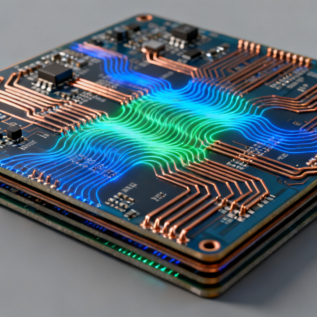
PCB Crosstalk refers to the transfer of energy from one signal trace (the aggressor) to an adjacent trace (the victim) via parasitic electromagnetic fields. It is an unintentional coupling mechanism that can corrupt intended signals, leading to false switching, data errors, and degraded noise margins.
Key Terminology
- Aggressor Line: The trace carrying the signal that induces unwanted voltage.
- Victim Line: The trace that receives the unwanted coupled energy.
- Near-End Crosstalk (NEXT): Noise measured at the victim line end closest to the aggressor driver.
- Far-End Crosstalk (FEXT): Noise measured at the victim line end farthest from the aggressor driver.
The Physics of PCB Crosstalk – How It Happens
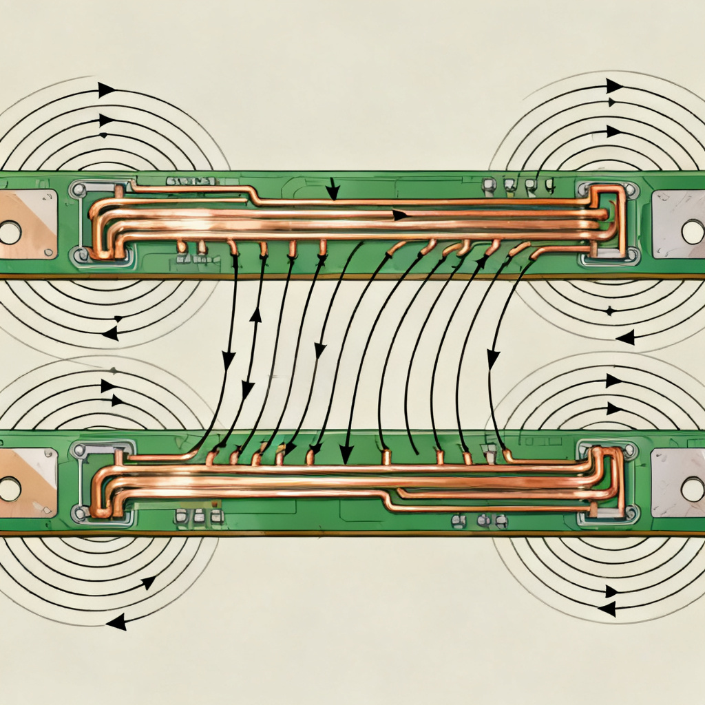
PCB Crosstalk arises from three distinct coupling mechanisms: capacitive, inductive, and common impedance coupling.
Capacitive (Electric) Coupling
A changing voltage on the aggressor trace creates a time-varying electric field that couples to the victim trace through parasitic capacitance. The magnitude is proportional to dV/dt and mutual capacitance (Cm).
Inductive (Magnetic) Coupling
A changing current on the aggressor trace generates a magnetic field that induces voltage in the victim trace through mutual inductance (Lm). This is dominant in low-impedance circuits and is a primary cause of FEXT.
Common Impedance Coupling
When two circuits share a common return path, current from one circuit creates a voltage drop across the shared impedance, appearing as noise for the other circuit. Use separate return paths and star grounding to mitigate.
Radiated Coupling
At GHz frequencies, traces can act as antennas. Proper shielding and enclosure design are required for RF and microwave applications.
Effects of PCB Crosstalk – Why You Should Care
PCB Crosstalk has real-world consequences that can destroy product performance.
Functional Effects
- False Switching (Glitches): A strong crosstalk pulse can momentarily exceed logic thresholds, causing false clock edges or data corruption.
- Timing Jitter: Crosstalk shifts signal zero-crossing points, reducing timing margins and causing setup/hold violations.
- Reduced Noise Margin: Continuous crosstalk noise shrinks the voltage window between valid logic states.
- Signal Distortion: Crosstalk adds ringing, overshoot, and undershoot to signals.
System-Level Effects
- EMI/EMC Failures: Crosstalk can cause excessive electromagnetic interference, failing regulatory compliance tests.
- Power Integrity Issues: Crosstalk on power distribution networks causes voltage ripple affecting sensitive analog blocks.
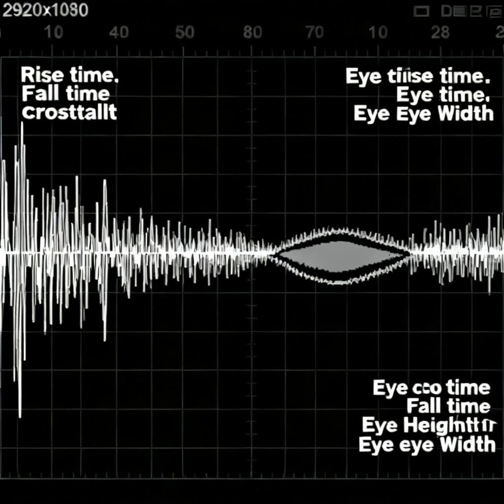
- Data Eye Closure: In high-speed serial links, crosstalk directly closes the data eye diagram, increasing bit error rate.
Analog & Mixed-Signal Effects
- Noise in Analog Circuits: Digital switching noise from crosstalk reduces SNR in precision analog circuits.
- Clock Feedthrough: A clock line near an analog trace can couple switching edges into the analog path.
Quantifying PCB Crosstalk – Key Parameters
To effectively mitigate PCB Crosstalk, you must measure and model it using these parameters:
| Parameter | Description |
|---|---|
| Coupling Coefficient (K) | Dimensionless number (0 to 1) describing energy transfer fraction from aggressor to victim. |
| Mutual Capacitance (Cm) | Parasitic capacitor between two traces, proportional to trace overlap area and inversely proportional to distance. |
| Mutual Inductance (Lm) | Parasitic inductor formed by the loop between two traces, influenced by return path geometry. |
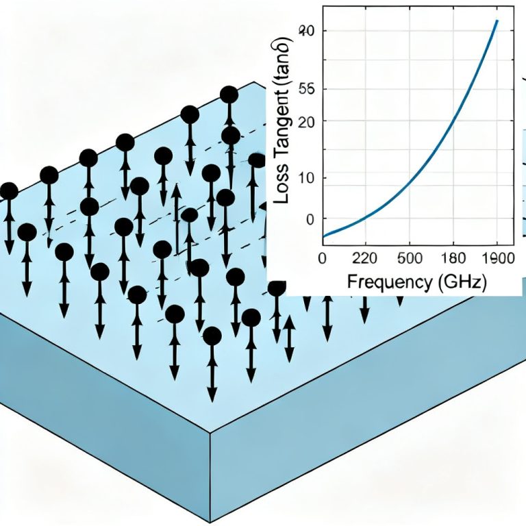
| Dielectric Constant (Dk) | Higher Dk materials increase capacitive coupling; lower Dk materials reduce it. |
| Rise Time (Tr) | The single most important factor—faster rise times contain higher-frequency components that couple more efficiently. |
| Trace Geometry | Width (W), spacing (S), length (L), and thickness (T) all affect coupling magnitude. |
PCB Crosstalk Mitigation Strategies
This section merges all unique mitigation techniques from top sources, organized by design stage.
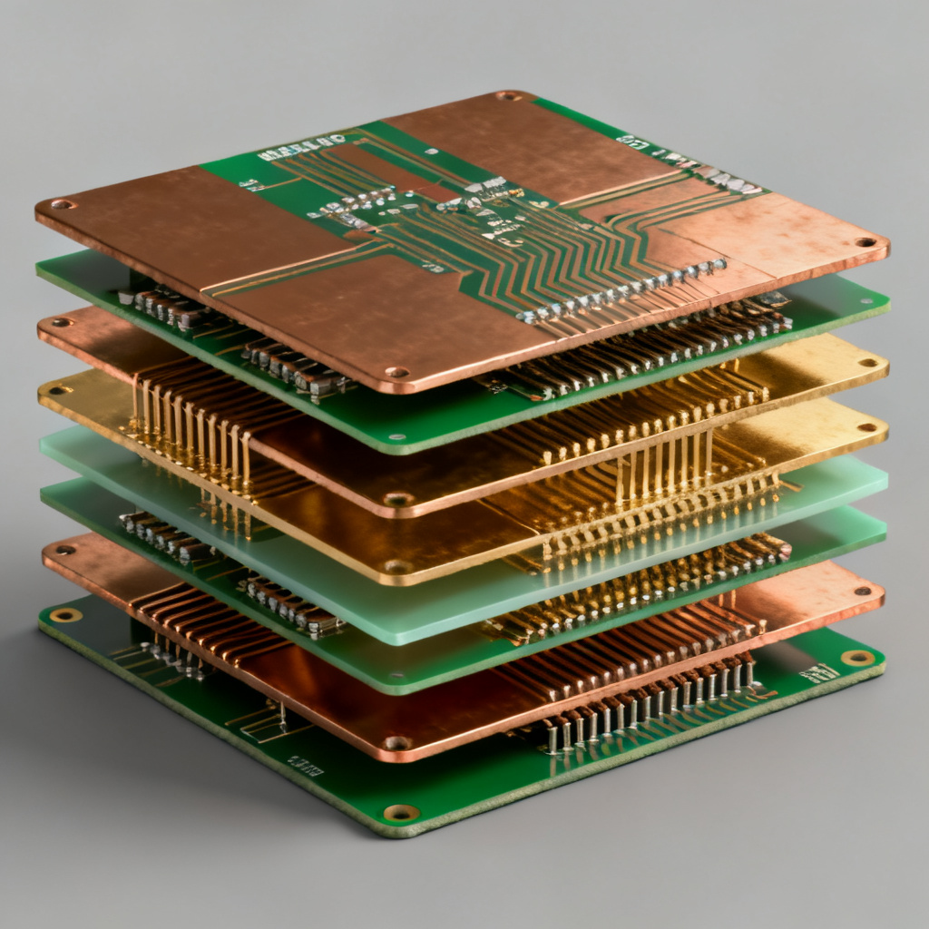
PCB Stackup & Layer Management
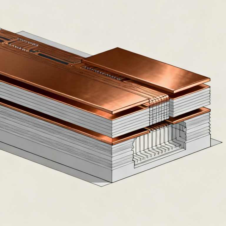
- Use a Solid Ground Plane: Provides low-impedance return path, minimizing loop area and inductive coupling.
- Microstrip vs. Stripline: Stripline offers far better isolation than microstrip—use for critical high-speed signals.
- Dedicated Power/Ground Layers: Creates natural shield between signal layers.
- Layer Ordering: Place high-speed signal layers adjacent to ground plane; avoid placing two high-speed layers next to each other.
Trace Routing Techniques
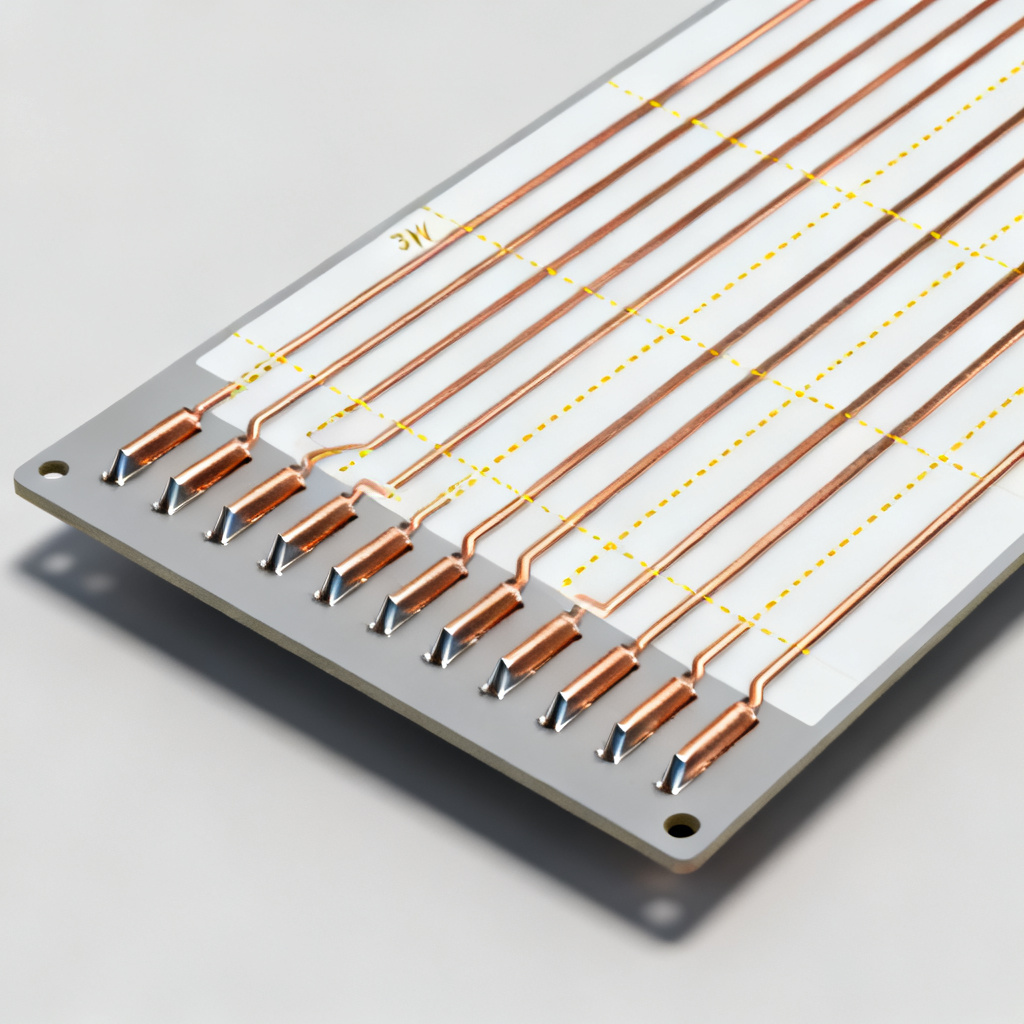
- Increase Trace Spacing (3W Rule): The most effective single technique—spacing at least 3x trace width; use 5W or 10W for aggressive crosstalk.
- Minimize Parallel Lengths: Route high-speed traces in short, direct paths.
- Use Guard Traces: Place grounded trace between signal traces; stitch to ground plane with vias every λ/10.
- Avoid 90-Degree Corners: Use 45-degree chamfers or curved traces to reduce capacitive coupling.
- Differential Pair Routing: Route with controlled impedance and tight coupling for common-mode rejection.
- Separate Analog and Digital: Physically separate sections; use ground-plane moat if necessary.
Impedance Control & Termination
- Controlled Impedance: Design traces to specific impedance (e.g., 50Ω single-ended, 100Ω differential) to minimize reflections.
- Series Termination: Place resistor near driver to dampen signal energy.
- Parallel Termination: Place resistor to ground or VCC at receiver to absorb signal energy.
- AC Termination: Use capacitor in series with resistor to ground for reducing power consumption while terminating high-frequency components.
Advanced Mitigation Techniques
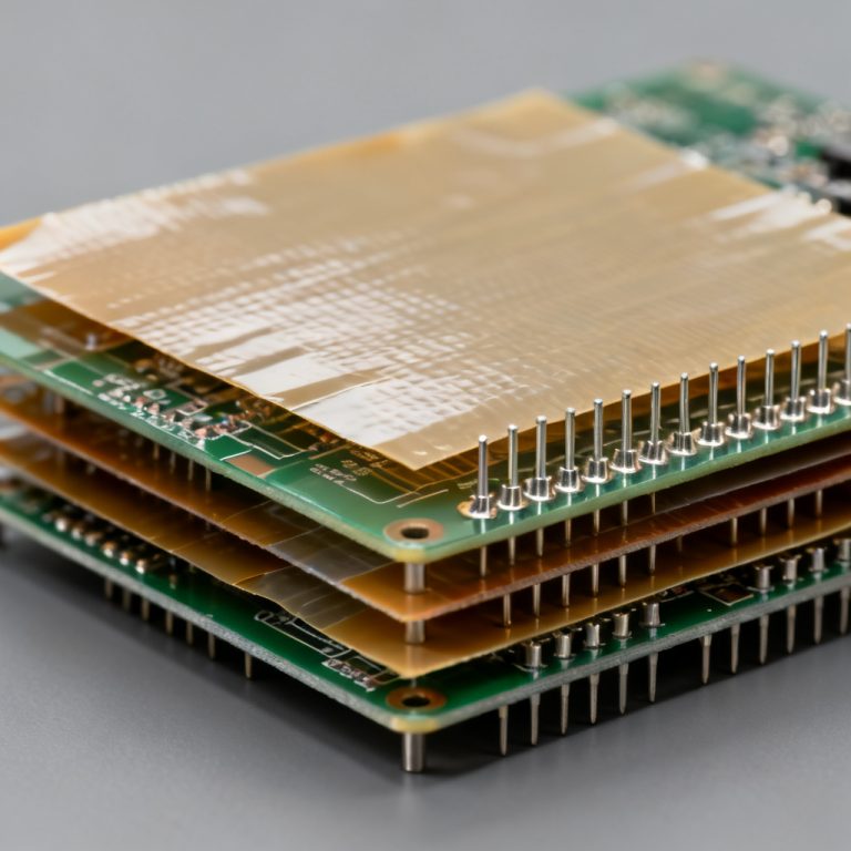
- Stitching Vias: Place vias around high-speed region perimeter to confine fields.
- Differential Pair Skew Compensation: Ensure identical path lengths for both legs.
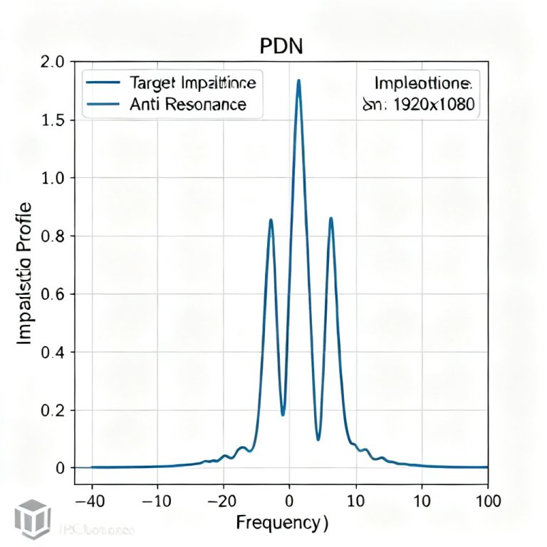
- Power Plane Decoupling: Use bulk and high-frequency decoupling capacitors for low-impedance PDN.
- Use of Lower Dk Materials: Switch from FR4 to low-Dk materials (Rogers, Isola) for extreme high-speed designs.
- Via Stub Removal: Use back-drilling or blind/buried vias to eliminate resonant stubs.
Simulation & Verification
- Pre-layout Simulation: Use tools like HyperLynx, ADS, or SiWave to model crosstalk before layout.
- Post-layout Simulation: Extract S-parameters and simulate with real-world drivers.
- Time-Domain Reflectometry (TDR): Measure impedance discontinuities and crosstalk on prototypes.
- Eye Diagram Analysis: Measure data eye at receiver to quantify jitter and eye closure.
Real-World PCB Crosstalk Case Studies
High-Speed Digital Bus
A 16-bit parallel bus at 800 MHz failed due to data corruption. Traces had only 4 mil spacing over 3 inches on an outer layer. FEXT exceeded 200 mV. Solution: Moved to inner stripline layer, increased spacing to 12 mils, added series termination. Crosstalk dropped below 20 mV.
Mixed-Signal ADC
A 24-bit ADC exhibited 10-bit noise floor. A digital clock line was routed directly under analog input traces. Solution: Re-routed clock to different layer, inserted ground plane between analog and digital sections, added guard trace. Noise floor dropped to 22-bit performance.
Automotive Camera Module
An automotive camera module failed EMI testing at 1.2 GHz. Crosstalk between LVDS data lines and power supply traces created common-mode noise radiating from cable. Solution: Added ferrite beads on power lines, re-routed LVDS pair with tighter coupling and dedicated ground plane, added stitching vias. EMI passed.
PCB Crosstalk Design Rules of Thumb
| Rule | Description |
|---|---|
| 3W Rule | Trace spacing ≥ 3x trace width for minimal crosstalk. |
| 10x Height Rule | Keep traces at least 10x dielectric height away from any via or component. |
| 20H Rule | Keep power plane edges at least 20x dielectric height away from signal traces. |
| Guard Trace Spacing | Guard trace width at least 2x signal trace width. |
| Via Stub Length | Keep via stubs shorter than 1/10th of signal’s rise time wavelength. |
Frequently Asked Questions About PCB Crosstalk
What is PCB Crosstalk and why does it matter?
PCB Crosstalk is unwanted electromagnetic coupling between adjacent traces that degrades signal integrity, causing false switching, jitter, and EMI issues in high-speed designs.
How can I reduce PCB Crosstalk in my design?
Increase trace spacing (3W rule), use solid ground planes, minimize parallel trace lengths, employ guard traces, and implement controlled impedance with proper termination.
What is the difference between NEXT and FEXT in PCB Crosstalk?
NEXT (Near-End Crosstalk) is noise measured at the victim line end closest to the aggressor driver, while FEXT (Far-End Crosstalk) is measured at the farthest end. FEXT is more problematic in high-speed designs.
Does PCB Crosstalk affect analog circuits differently?
Yes, analog circuits are more sensitive to crosstalk noise. Digital switching noise can significantly reduce SNR in precision analog circuits like ADCs and op-amps.
What simulation tools are best for analyzing PCB Crosstalk?
Industry-standard tools include HyperLynx, ADS, and SiWave for pre-layout and post-layout simulation, along with TDR measurements for prototype verification.
Conclusion: The Path to Zero-Crosstalk Designs
PCB Crosstalk is a complex but solvable problem. By understanding its physical origins, quantifying its effects, and applying systematic mitigation strategies—from stackup design to simulation—you can achieve robust, high-performance designs.
Key Takeaways for B2B Buyers:
- For PCB Manufacturers: A partner who understands crosstalk will design stackups, control impedance, and verify signal integrity. Look for certifications like IPC-6012 and experience with high-speed materials.
- For Design Engineers: Always simulate crosstalk before fabrication. The cost of a simulation tool is negligible compared to a board re-spin.
- For Procurement: Specify controlled impedance, a defined stackup, and a requirement for crosstalk simulation reports in your PCB fabrication order.
Final Pro-Tip: The single most effective and cheapest way to reduce PCB Crosstalk is increasing trace spacing. Before adding guard traces, changing materials, or complex terminations, simply move your traces farther apart. It works every time.