Drilling and Backdrilling for PCB Through Holes
In modern PCB manufacturing, drilling and backdrilling for PCB through holes is a critical process that directly impacts signal integrity and reliability. This guide covers everything from drill bit selection to backdrilling depth control, ensuring your high‑speed designs perform flawlessly.
1. Introduction: Why Drilling and Backdrilling Matter in Modern PCBs
In high‑density interconnect (HDI) and high‑speed digital designs, the humble through‑hole is far from simple. Drilling and backdrilling for PCB through‑holes is the foundation of all plated through‑holes (PTHs), vias, and component mounting holes. Backdrilling, a specialized post‑drilling process, removes unused portions of via stubs that cause signal reflections, impedance discontinuities, and electromagnetic interference (EMI) at GHz frequencies.
This pillar page covers everything from drill bit geometry and stack‑up considerations to backdrilling depth control, quality verification, and cost implications. Whether you are designing a 20‑layer server board or a 4‑layer IoT module, understanding these processes ensures first‑pass success and reliable performance.
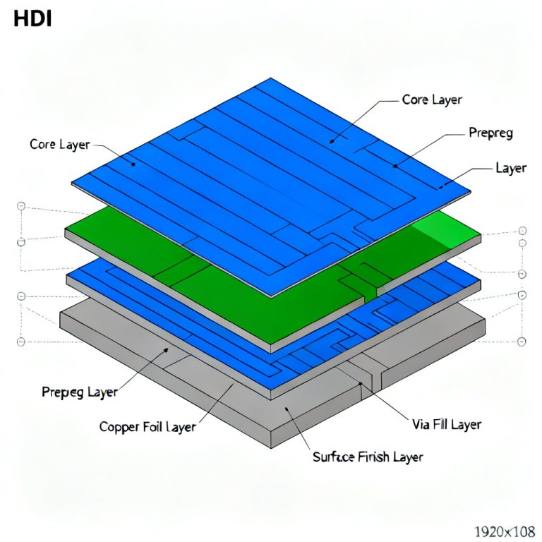
2. The Fundamentals of PCB Drilling for Through‑Holes
2.1 Types of Holes Created by Drilling
- Through‑Holes (PTHs): Plated holes connecting all layers, used for component leads and vias.
- Blind Vias: Connect an outer layer to one or more inner layers, but not through the entire board.
- Buried Vias: Connect inner layers only, invisible from the surface.
- Microvias: Small (<150 µm) blind vias typically laser‑drilled in HDI designs.
- Mounting Holes: Non‑plated holes for mechanical fastening.
2.2 Drill Bit Materials and Geometry
- Tungsten Carbide (WC): The industry standard for most PCBs due to its hardness and wear resistance. Grain size (0.5–1.0 µm) affects edge sharpness.
- Diamond‑Coated Bits: Used for high‑volume production or drilling ceramic‑filled laminates (e.g., Rogers, Teflon).
- Bit Geometry: Standard point angle is 130° for FR‑4; shallower angles (120°) for softer materials, steeper (140°) for rigid ceramics. Helix angle (30–45°) influences chip evacuation.
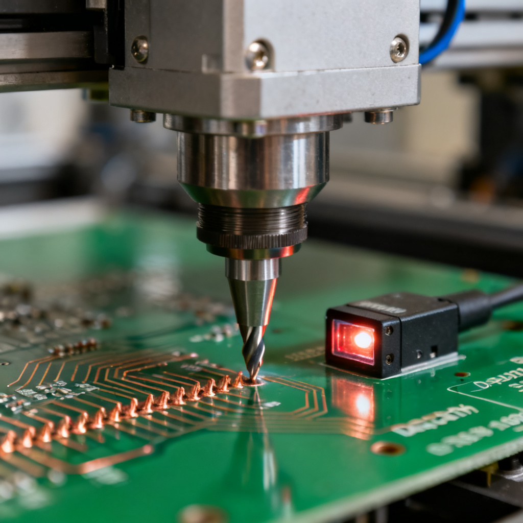
2.3 Drilling Parameters
- Spindle Speed: Typically 80,000–150,000 RPM for small bits (<0.3 mm), down to 20,000–40,000 RPM for larger bits (>1.0 mm).
- Feed Rate: 50–200 mm/min depending on material and hole size. Too fast risks bit breakage; too slow causes excessive heat and resin smear.
- Retraction Speed: Controlled to avoid pulling debris back into the hole.
- Entry and Exit Materials: Aluminum entry foil reduces burr formation; phenolic backup board prevents exit‑side breakout.
2.4 Stack‑Up Considerations for Drilling
- Drill‑to‑Copper Clearance: Minimum 0.2 mm for standard boards; 0.15 mm for high‑density designs to avoid drill wander.
- Aspect Ratio: Ratio of board thickness to hole diameter. For mechanical drilling, max aspect ratio is typically 10:1 (e.g., 1.6 mm board with 0.2 mm hole). Higher ratios require laser drilling or sequential lamination.
- Layer Registration: Inner layer pads must align with drilled holes within ±0.05 mm (2 mil) tolerance.
2.5 Common Drilling Defects and How to Avoid Them
- Nailheading: Flaring of copper at the hole edge due to dull bits or excessive heat. Solution: replace bits after 2,000–3,000 hits.
- Resin Smear: Melted resin coating inner copper layers, causing poor electrical connection. Solution: optimize drilling parameters and use desmear (plasma/chemical) after drilling.
- Burr Formation: Raised copper around hole edges. Solution: use entry/exit materials and sharp bits.
- Drill Breakage: Caused by high feed rate, worn bits, or contaminated material. Solution: implement tool‑life monitoring and automated bit change.
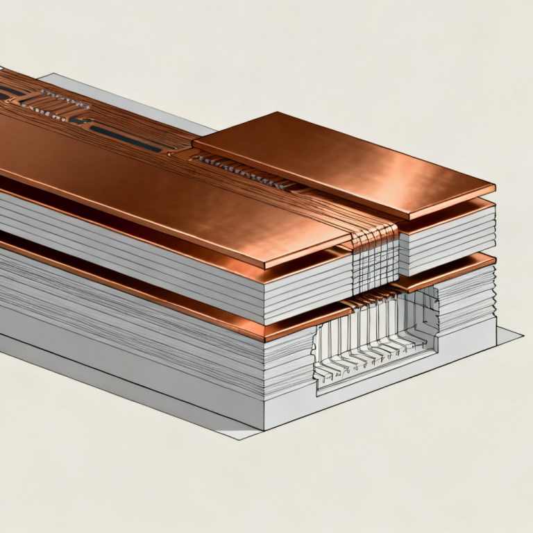
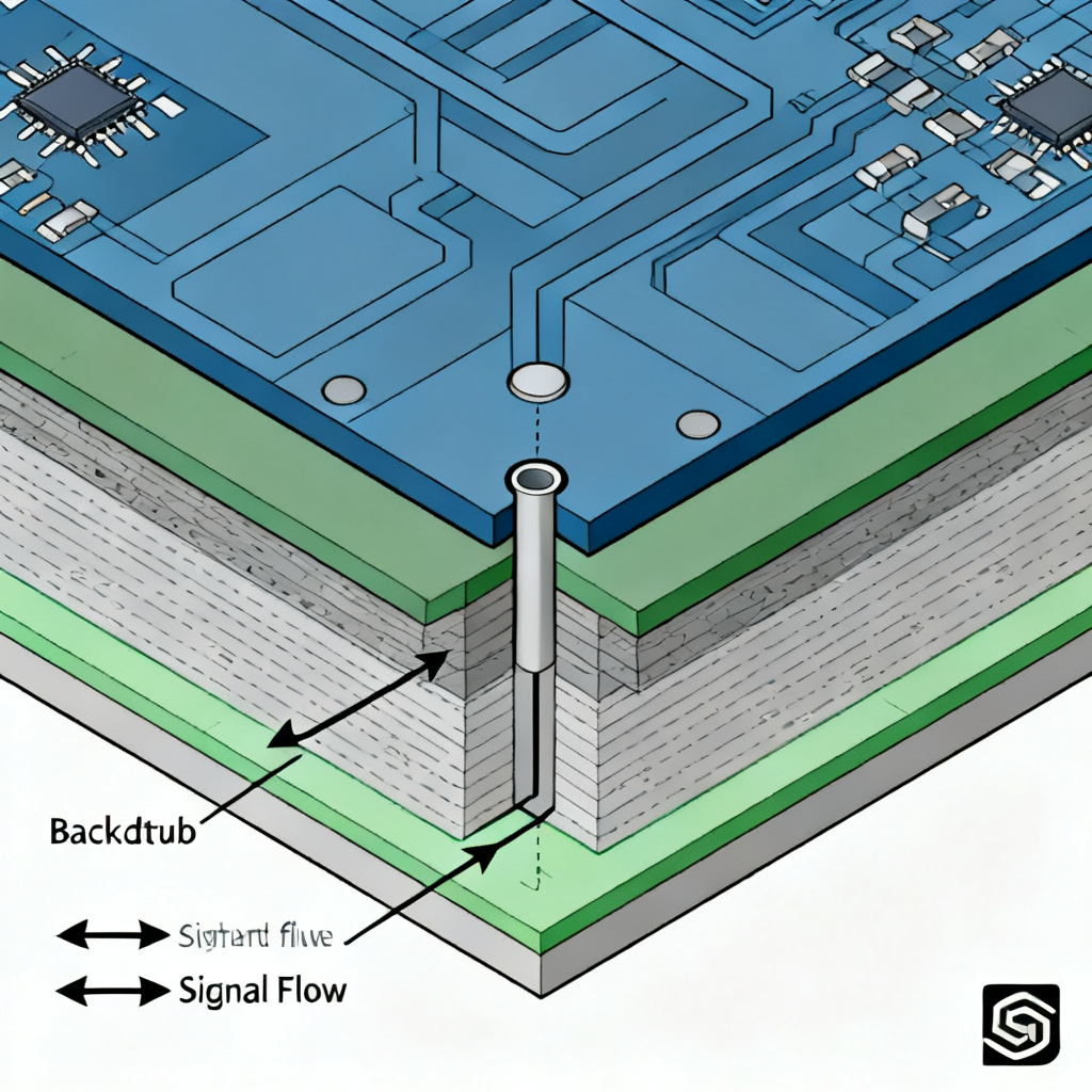
3. Backdrilling for PCB Through‑Holes: The Advanced Process for High‑Speed Signals
3.1 What Is Backdrilling and Why Is It Necessary?
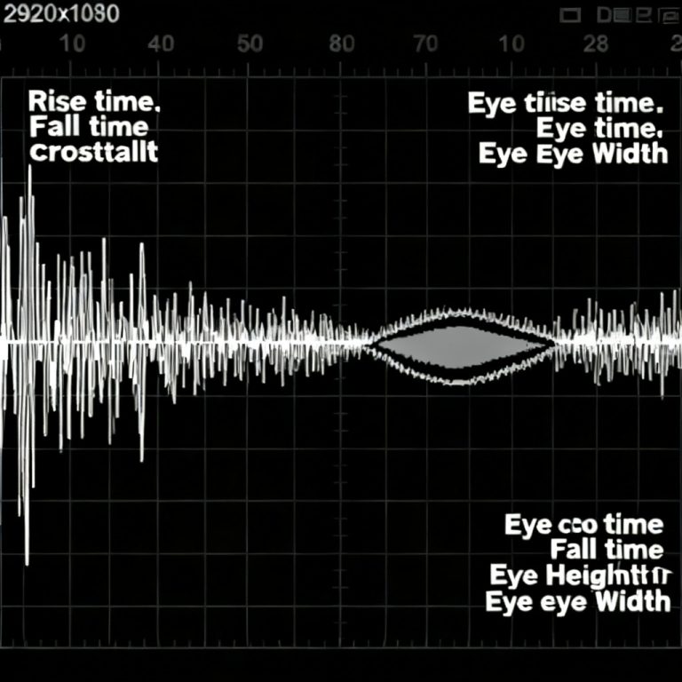
Backdrilling for PCB through‑holes (also called controlled‑depth drilling) removes the unused, non‑functional portion of a through‑hole via that extends beyond the signal layer transition. This “via stub” acts as a transmission line stub, causing:
- Signal reflections at high frequencies (above 1 GHz).
- Impedance discontinuities that degrade eye diagrams.
- Resonant frequencies that amplify noise (e.g., at 1/4 wavelength).
- Increased EMI due to stub radiation.
By backdrilling, you eliminate the stub, preserving signal integrity up to 40 GHz and beyond.
3.2 The Backdrilling Process Step by Step
- Initial Drilling: The entire through‑hole is drilled to full board thickness (standard PTH process).
- Plating: Electroless and electrolytic copper plate the hole wall.
- First Etch: Outer layer copper is etched to form pads and traces.
- Backdrilling: A larger‑diameter drill bit (typically 0.1–0.2 mm larger than the original hole) drills from the bottom side of the board to a precise depth, removing the copper plating and the unused via stub.
- Second Etch (Optional): Removes any burrs or copper debris left by backdrilling.
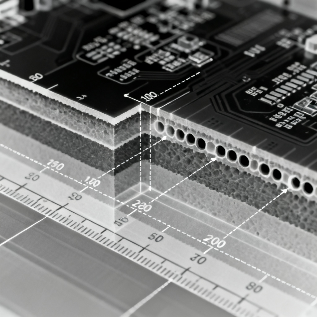
- Final Inspection: Depth and cleanliness verified via X‑ray or cross‑section.
3.3 Depth Control and Tolerances
- Target Depth: The backdrill depth must stop exactly at the last signal layer that uses the via. A common tolerance is ±0.05 mm (±2 mil).
- Stub Length Remaining: Ideally <0.1 mm (4 mil) for high‑speed designs. Longer stubs (0.2 mm) may still cause resonance at 10+ GHz.
- Methods of Control:
- Mechanical Depth Stops: Used on standard CNC drills; accuracy ±0.1 mm.
- Laser Depth Sensing: Real‑time measurement for ±0.025 mm accuracy.
- X‑Ray Feedback: Post‑drill measurement to adjust subsequent runs.
3.4 Materials and Drill Bit Selection for Backdrilling
- Bit Material: Same tungsten carbide as standard drills, but with a longer flute length to clear copper chips.
- Bit Diameter: Typically 0.2–0.3 mm larger than the original hole to ensure complete removal of the plated copper.
- Entry/Exit Materials: Thicker entry foil (0.3 mm) to prevent bit wander; phenolic backup board to support exit.
3.5 Design Rules for Backdrilling
- Minimum Annular Ring: The pad on the bottom layer must be at least 0.2 mm larger than the backdrill bit diameter to avoid damaging functional pads.
- Layer Separation: The distance between the last signal layer and the backdrill stop layer should be >0.15 mm to avoid shorting.
- Avoid Backdrilling Near Connectors: Mechanical stress from the backdrill bit can damage nearby press‑fit holes.
- Stack‑Up Symmetry: For boards with multiple backdrilled layers, ensure symmetrical layer pairs to balance copper removal and prevent warpage.
3.6 Backdrilling vs. Other Via Stub Mitigation Techniques
| Backdrilling for PCB Through‑Holes Technique | Stub Removal | Cost | Complexity | Max Frequency |
|---|---|---|---|---|
| Backdrilling | Partial (stub <0.1 mm) | Moderate | Moderate | Up to 40 GHz |
| Buried Vias | Complete | High | High | Unlimited |
| Microvias (HDI) | Complete | Very High | High | Up to 100 GHz |
| Via Filling (e.g., conductive paste) | Partial | Low | Low | Up to 10 GHz |
| Staggered Vias | Partial | Moderate | Moderate | Up to 20 GHz |
4. Quality Control and Testing for Drilling and Backdrilling
4.1 Visual and Dimensional Inspection
- Microscope Inspection: Check for burrs, copper flakes, and depth consistency on sample coupons.
- Cross‑Sectioning: Destructive test of a production panel to measure backdrill depth, stub length, and copper plating thickness.
- X‑Ray Inspection: Non‑destructive method to verify backdrill depth and alignment with inner layers.
4.2 Electrical Testing
- Time Domain Reflectometry (TDR): Measures impedance changes caused by remaining stubs. A clean TDR trace indicates successful backdrilling.
- Vector Network Analyzer (VNA): S‑parameter measurements (S11, S21) confirm reduced reflections and insertion loss.
- Continuity and Isolation Testing: Ensures backdrilling did not break functional connections.
4.3 Reliability Testing
- Thermal Cycling: -55°C to +125°C for 100 cycles to check for micro‑cracks at the backdrill interface.
- Plating Adhesion: Peel test on backdrilled inner walls to ensure copper remains bonded.
- Hole Wall Roughness: Measured via profilometry; target <10 µm Ra for high‑reliability designs.
5. Cost and Lead Time Implications of Backdrilling for PCB Through‑Holes
5.1 Cost Drivers for Backdrilling
- Number of Backdrilled Layers: Each additional layer requires a separate drill pass and increased setup time.
- Board Thickness: Thicker boards require slower feed rates and more expensive long‑flute bits.
- Tolerance Requirements: Tighter depth tolerances (±0.025 mm) require laser‑guided systems, increasing cost by 20–30%.
- Material Type: PTFE or ceramic‑filled laminates wear bits faster, raising tooling costs.
5.2 Typical Cost Premium
- Standard PCB (no backdrilling): Baseline.
- Backdrilled PCB (1–2 layers): +15–25% over standard cost.
- Backdrilled PCB (3+ layers): +30–50%.
- HDI with backdrilling: +50–100% due to complexity.
5.3 Lead Time Impact
- Standard drilling: 1–2 days.
- Backdrilling: Adds 1–3 days for depth setup, inspection, and rework if needed.
- Rush orders: Possible with 2–3 day turnaround but at 2x cost.
6. Design for Manufacturability (DFM) Checklist for Drilling and Backdrilling
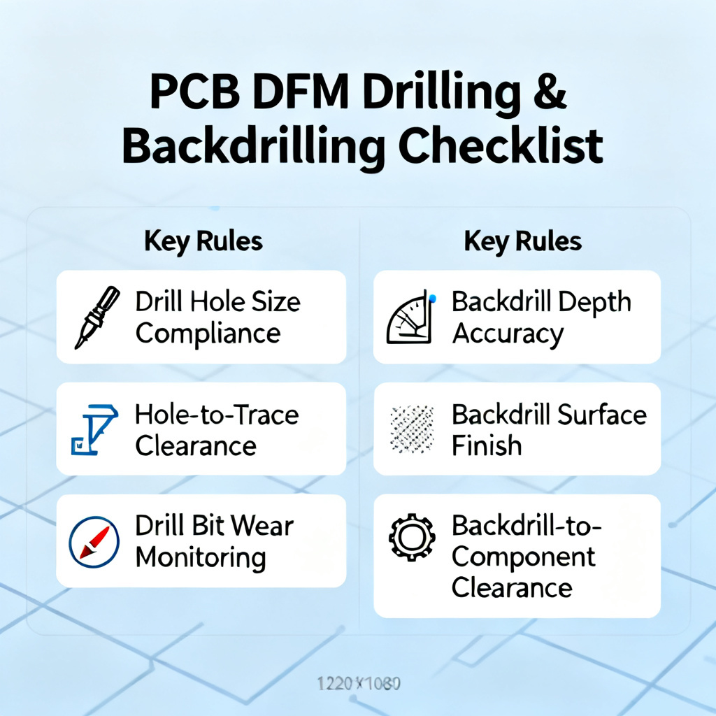
- [ ] Specify backdrill depth, bit diameter, and tolerance in your fabrication drawing.
- [ ] Ensure annular ring on the stop layer is ≥0.2 mm larger than backdrill bit.
- [ ] Avoid placing backdrilled vias within 1 mm of board edges or high‑stress areas.
- [ ] Use symmetrical backdrill patterns to prevent board warpage.
- [ ] Include test coupons on the panel for cross‑sectioning.
- [ ] Communicate signal layer transitions clearly to the fabricator.
- [ ] For frequencies >10 GHz, request stub length <0.05 mm.
7. Frequently Asked Questions (FAQ) About Drilling and Backdrilling for PCB Through‑Holes
Can backdrilling for PCB through‑holes be performed on any PCB material?
What is the minimum hole size that can be backdrilled for PCB through‑holes?
Does backdrilling affect the mechanical strength of the board?
How do I verify backdrill depth without destroying the board?
Can backdrilling for PCB through‑holes be combined with via filling?
8. Conclusion: Partner with an Expert for High‑Speed Success
Drilling and backdrilling for PCB through‑holes are not just manufacturing steps—they are critical enablers of signal integrity, reliability, and miniaturization in modern PCBs. By understanding the nuances of drill bit selection, depth control, and DFM rules, you can avoid costly redesigns and achieve first‑pass success for designs up to 40 GHz and beyond.
When you choose our factory for your next PCB project, you gain access to:
- Advanced CNC drills with laser depth sensing (±0.025 mm accuracy).
- Automated X‑ray inspection for 100% backdrill verification.
- Experienced engineering team to review your stack‑up and backdrill requirements.
- Fast turnaround (5–7 days for standard backdrilled boards).
Request a quote today and let us help you turn your high‑speed design into a reliable, manufacturable reality.
This pillar page is updated quarterly to reflect the latest IPC standards (IPC‑6012, IPC‑4761) and industry best practices. Last revision: October 2023.