Copper Plating Electroless and Electrolytic
Copper Plating – Electroless and Electrolytic for PCB Manufacturing
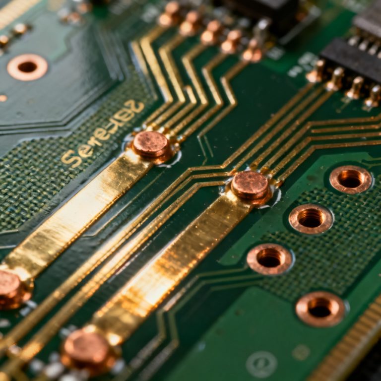
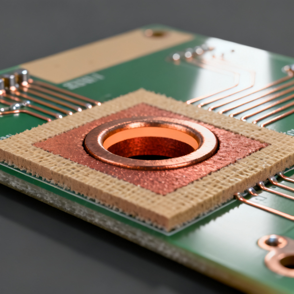
Copper plating electroless and electrolytic – is a cornerstone process in PCB manufacturing, enabling conductive pathways, through-hole vias, and surface finishes. It is divided into two primary methods: electroless copper plating (chemical copper) and electrolytic copper plating (electroplating).
1. Introduction to Copper Plating in PCB Manufacturing
Copper plating – electroless and electrolytic – is essential for interconnecting layers in multi-layer PCBs, providing reliable electrical conductivity and thermal management. In modern PCB production, the process typically follows a sequence: electroless copper plating is first used to deposit a thin, uniform layer of copper (typically 0.5–1.5 µm) on non-conductive substrates (e.g., drilled hole walls and laminate surfaces). This layer serves as a conductive seed for subsequent electrolytic copper plating, which builds the copper thickness to the required specification (often 15–50 µm or more, depending on the PCB class). Without electroless copper, electroplating cannot occur on non-conductive surfaces, making it a critical enabling technology.
2. Electroless Copper Plating (Chemical Copper)
2.1. Definition and Principle of Electroless Copper Plating
Electroless copper plating is a controlled autocatalytic chemical reduction process. It deposits copper from a solution onto a catalytic surface without the need for an external electrical current. The reaction is driven by a reducing agent (typically formaldehyde or newer alternatives like glyoxylic acid) that reduces copper ions (Cu²⁺) to metallic copper (Cu⁰) on the substrate. The deposition is self-sustaining once initiated, as the deposited copper itself acts as a catalyst for further reduction.
2.2. Chemistry and Key Components of Electroless Copper Plating
The electroless copper bath contains several essential components:
- Copper Source: Typically copper sulfate (CuSO₄·5H₂O) provides the copper ions.
- Reducing Agent: Formaldehyde (HCHO) is the most common, though it is toxic and increasingly regulated. Alternative systems use glyoxylic acid or sodium hypophosphite.
- Complexing Agents: EDTA (ethylenediaminetetraacetic acid) or tartrates keep copper ions in solution at alkaline pH (12–13) and prevent precipitation.
- Stabilizers: Small amounts of sulfur compounds or cyanide derivatives prevent spontaneous decomposition of the bath.
- pH Adjusters: Sodium hydroxide (NaOH) maintains the high pH required for the reaction.
- Accelerators and Wetting Agents: Improve deposition rate and uniformity.
The overall simplified reaction with formaldehyde is: Cu²⁺ + 2HCHO + 4OH⁻ → Cu⁰ + 2HCOO⁻ + H₂↑ + 2H₂O
2.3. Process Sequence for Electroless Copper Plating
The electroless copper plating process involves multiple pretreatment steps to ensure adhesion and uniformity:
- Cleaning and Conditioning: Removal of organic residues and surface activation using a mild alkaline cleaner or conditioner.
- Micro-etching: A mild sulfuric acid/peroxide or ammonium persulfate solution roughens the copper surface (if present) to improve adhesion.
- Catalyzation (Activation): The substrate is immersed in a palladium-tin colloid solution. Palladium ions are adsorbed onto the surface, serving as catalytic nuclei for copper deposition. This step is critical for non-conductive surfaces like FR-4.
- Acceleration: A dilute acid or alkaline solution removes excess tin from the palladium-tin complex, exposing the catalytic palladium.
- Electroless Copper Deposition: The board is immersed in the electroless copper bath at a controlled temperature (typically 40–50°C) for 15–30 minutes to achieve the desired thickness.
- Rinsing and Drying: Thorough rinsing with deionized water removes residual chemicals.
2.4. Equipment and Configuration for Electroless Copper Plating
Electroless copper lines are typically horizontal or vertical immersion systems with:
- Heated Tanks: Polypropylene or PVC tanks with precise temperature control (±1°C).
- Filtration Systems: Continuous filtration (1–5 µm) removes particles and prevents bath contamination.
- Automatic Dosing: Sensors monitor copper concentration, pH, and stabilizer levels, automatically replenishing chemicals.
- Rinse Stations: Cascade or spray rinses to minimize drag-out and cross-contamination.
2.5. Advantages and Limitations of Electroless Copper Plating
Advantages:
- Deposits uniformly on all surfaces, including non-conductive substrates and complex geometries.
- No need for electrical connections, enabling plating of through-holes and blind vias.
- Excellent step coverage and adhesion to dielectric materials.
Limitations:
- Slower deposition rate (0.1–0.3 µm/min) compared to electrolytic plating.
- Bath chemistry is sensitive to contamination and requires careful maintenance.
- Formaldehyde-based baths pose health and environmental risks; alternative chemistries are emerging but may have different performance characteristics.
- Higher operating costs due to chemical consumption and waste treatment.
2.6. Quality Control and Troubleshooting for Electroless Copper Plating
Key quality parameters include:
- Thickness: Measured by X-ray fluorescence (XRF) or cross-sectioning; typical target is 0.5–1.5 µm.
- Adhesion: Tape test or pull test to ensure no peeling.
- Coverage: Visual inspection under microscope for voids or skip plating.
- Bath Stability: Conductivity, pH, and copper concentration monitored hourly.
Common defects:
- Skip Plating: Incomplete coverage due to poor catalyzation or bath depletion.
- Roughness: Caused by excessive stabilizer or contamination.
- Slow Deposition: Low temperature, low copper concentration, or high stabilizer level.
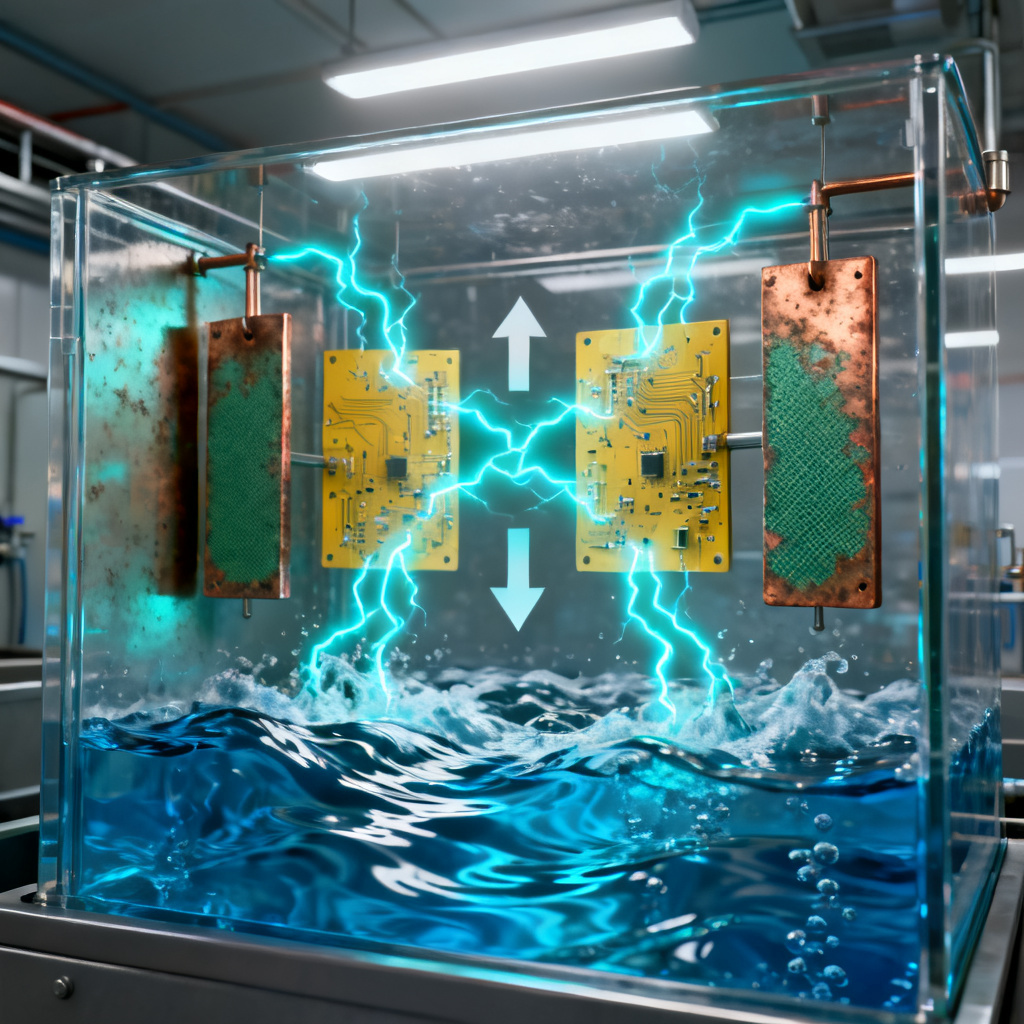
3. Electrolytic Copper Plating (Electroplating)
3.1. Definition and Principle of Electrolytic Copper Plating
Electrolytic copper plating uses an external electrical current to reduce copper ions (Cu²⁺) from a solution onto a conductive surface (the PCB panel). The PCB acts as the cathode (negative electrode), while a copper anode (typically oxygen-free copper or phosphorized copper) provides the copper source. The process is governed by Faraday’s laws: the mass of copper deposited is proportional to the current, time, and current efficiency.
3.2. Chemistry and Key Components of Electrolytic Copper Plating
The electrolytic copper bath is typically based on an acid copper sulfate system:
- Copper Sulfate (CuSO₄·5H₂O): 60–100 g/L provides copper ions.
- Sulfuric Acid (H₂SO₄): 180–220 g/L increases conductivity and prevents hydrolysis.
- Chloride Ions (Cl⁻): 50–100 ppm as HCl improves anode dissolution and deposit structure.
- Organic Additives: Three main categories:
- Brighteners (Carriers): Polyethylene glycol (PEG) or similar suppress copper deposition at high current density areas.
- Levelers: Sulfur-containing compounds (e.g., Janus Green B) promote uniform deposition.
- Accelerators: Sulfur-based molecules (e.g., Bis-(3-sulfopropyl) disulfide, SPS) enhance deposition at low current density areas.
These additives work synergistically to produce a bright, ductile, and fine-grained copper deposit.
3.3. Process Sequence for Electrolytic Copper Plating
After electroless copper deposition, the PCB undergoes:
- Pre-cleaning: Acidic cleaner removes oxides and residues from the electroless copper layer.
- Micro-etching: A mild sulfuric acid/peroxide solution removes a thin layer (0.5–1 µm) to ensure adhesion.
- Rinsing: Deionized water rinse.
- Electrolytic Plating: The PCB is immersed in the plating bath, connected to the cathode, and current is applied. Typical parameters:
- Current density: 1–4 A/dm²
- Temperature: 20–30°C
- Agitation: Air or solution agitation to ensure uniform ion distribution.
- Plating time: 30–90 minutes depending on target thickness.
- Post-plate Rinse: Thorough rinsing to remove residual acid and additives.
3.4. Equipment and Configuration for Electrolytic Copper Plating
- Rectifiers: DC power supplies with ripple control (<5% ripple) to ensure smooth deposits.
- Plating Tanks: PVC, polypropylene, or stainless steel with acid-resistant linings.
- Anodes: Phosphorized copper (0.04–0.06% phosphorus) to prevent passivation and ensure even dissolution.
- Agitation Systems: Air spargers, solution pumps, or cathode movement (e.g., vibration or rotation) to improve mass transfer.
- Filtration: Continuous filtration (1–5 µm) removes particles and organic breakdown products.
- Additive Dosing: Automated systems using CVS (Cyclic Voltammetric Stripping) or HPLC to monitor and replenish organic additives.
3.5. Advantages and Limitations of Electrolytic Copper Plating
Advantages:
- High deposition rate (1–5 µm/min), enabling thick copper layers quickly.
- Excellent control over thickness via current and time.
- Produces smooth, dense, and ductile copper with good electrical properties.
- Lower chemical cost per unit of copper deposited compared to electroless.
Limitations:
- Requires a conductive seed layer (electroless copper) on non-conductive surfaces.
- Current distribution can be uneven, leading to thickness variations (dog-boning effect) on high-aspect-ratio holes.
- Organic additives degrade over time, requiring careful monitoring and replenishment.
- High current densities can cause burning or nodule formation.
3.6. Quality Control and Troubleshooting for Electrolytic Copper Plating
Key parameters:
- Thickness: Measured by XRF, cross-section, or beta backscatter.
- Tensile Strength and Elongation: Typically >250 MPa and >15% for ductile copper.
- Hardness: Vickers hardness test (typically 100–150 HV).
- Surface Roughness: Profilometry or atomic force microscopy (AFM).
Common defects:
- Burning: Excessive current density at edges or high points.
- Roughness: Contamination or additive imbalance.
- Pitting: Gas bubbles trapped on the surface.
- Poor Thickness Uniformity: Inadequate agitation or anode configuration.
4. Comparison: Electroless vs. Electrolytic Copper Plating
| Feature | Electroless Copper Plating | Electrolytic Copper Plating |
|---|---|---|
| Driving Force | Chemical reduction | Electrical current |
| Substrate Requirement | Catalytic surface (non-conductive or conductive) | Conductive surface |
| Deposition Rate | 0.1–0.3 µm/min | 1–5 µm/min |
| Thickness Range | 0.5–1.5 µm (typical) | 5–100+ µm |
| Uniformity | Excellent, conformal | Good but current-dependent |
| Bath Complexity | High (multiple components, sensitive) | Moderate (acid copper with additives) |
| Cost | Higher per unit thickness | Lower per unit thickness |
| Environmental Impact | Formaldehyde toxicity; waste treatment required | Acid waste; copper recovery possible |
| Primary Application | Seed layer for through-hole plating | Final copper build-up for traces and vias |
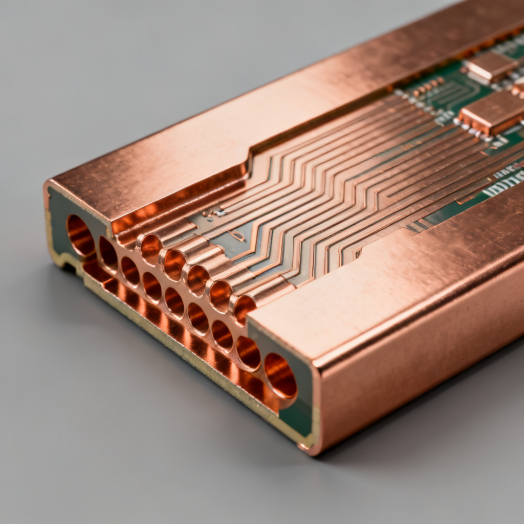
5. Applications in PCB Manufacturing
- Through-Hole Plating (THP): Both electroless and electrolytic copper are used to create conductive barrels in drilled holes, enabling electrical connection between layers.
- Blind and Buried Vias: Electroless copper is essential for plating non-conductive via walls in high-density interconnect (HDI) PCBs.
- Surface Finish Base Layer: Electroless copper is often the base for ENIG (Electroless Nickel Immersion Gold) or other finishes.
- Thick Copper PCBs: Electrolytic plating builds copper thickness for high-current applications (e.g., power electronics, automotive).
- Pattern Plating: In subtractive processes, electrolytic copper is selectively deposited on exposed circuit patterns.
6. Environmental and Safety Considerations
- Formaldehyde: A known carcinogen; electroless copper baths using formaldehyde require closed-loop systems, ventilation, and waste treatment. Alternatives (glyoxylic acid) are gaining traction.
- Palladium: Used in catalyzation; recovery and recycling reduce cost and environmental impact.
- Acid Waste: Electrolytic baths generate sulfuric acid waste; neutralization and metal recovery are standard.
- Additive Breakdown Products: Organic additives degrade over time; carbon filtration or batch treatment removes contaminants.
- Worker Safety: PPE (gloves, goggles, aprons) is mandatory; fume extraction and emergency showers are required.
7. Emerging Trends and Innovations
- Formaldehyde-Free Electroless Copper: Glyoxylic acid and sodium hypophosphite systems reduce toxicity but may require different stabilizers and operating conditions.
- High-Aspect-Ratio Plating: Improved agitation and additive systems enable plating of holes with aspect ratios >10:1.
- Pulse and Reverse Pulse Electroplating: Alternating current waveforms improve deposit uniformity and reduce porosity.
- Direct Metallization: Alternatives to electroless copper, such as conductive polymers or carbon-based processes, eliminate the need for palladium and formaldehyde.
- Automation and Industry 4.0: Real-time monitoring of bath chemistry (e.g., via UV-Vis spectroscopy, CVS) and AI-driven process optimization.
8. Conclusion
Copper plating – electroless and electrolytic – is indispensable for modern PCB manufacturing. Electroless copper provides the critical seed layer on non-conductive surfaces, ensuring reliable interconnection in multi-layer boards. Electrolytic copper builds the thick, conductive traces and via barrels that carry current and signals. Together, they form a synergistic process that enables the high-density, high-reliability PCBs required in aerospace, automotive, telecommunications, and consumer electronics. Understanding the chemistry, process control, and quality parameters of each method is essential for PCB manufacturers to achieve consistent, high-quality results. By mastering both electroless and electrolytic copper plating, you can optimize your production line, reduce defects, and meet the demanding specifications of today’s electronic designs.
FAQ: Copper Plating – Electroless and Electrolytic
What is the main difference between electroless and electrolytic copper plating?
The main difference is that electroless copper plating uses a chemical reduction process without external current, while electrolytic copper plating uses an electrical current. Electroless copper plating deposits a thin seed layer on non-conductive surfaces, and electrolytic copper plating builds thicker copper layers on conductive substrates.
Why is electroless copper plating essential for PCB manufacturing?
Electroless copper plating is essential because it deposits a uniform conductive layer on non-conductive surfaces like drilled hole walls, enabling subsequent electrolytic copper plating. Without it, through-hole vias and multi-layer interconnections would not be possible.
What are common defects in electrolytic copper plating?
Common defects in electrolytic copper plating include burning (excessive current density), roughness (contamination or additive imbalance), pitting (gas bubbles), and poor thickness uniformity (inadequate agitation or anode configuration).
How does copper plating impact PCB signal integrity?
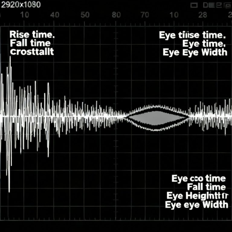
Copper plating directly affects signal integrity by ensuring uniform conductor thickness and low resistance. Electroless and electrolytic copper plating processes must be controlled to avoid voids, roughness, or thickness variations that can cause impedance discontinuities and signal loss.
{ “@context”: “https://schema.org”, “@type”: “BreadcrumbList”, “itemListElement”: [ { “@type”: “ListItem”, “position”: 1, “name”: “Home”, “item”: “https://pcbtypes.com/” }, { “@type”: “ListItem”, “position”: 2, “name”: “PCB Manufacturing Processes”, “item”: “https://pcbtypes.com/category/pcb-manufacturing-processes/” }, { “@type”: “ListItem”, “position”: 3, “name”: “Copper Plating – Electroless and Electrolytic”, “item”: “https://pcbtypes.com/copper-plating-electroless-and-electrolytic” } ] } { “@context”: “https://schema.org”, “@type”: “TechArticle”, “headline”: “Copper Plating – Electroless and Electrolytic for PCB Manufacturing”, “description”: “A comprehensive guide to electroless and electrolytic copper plating in PCB manufacturing, covering chemical principles, process sequences, and quality control.”, “image”: “https://pcbtypes.com/wp-content/uploads/pcb-through-hole-copper-plating-cross-section.jpg”, “author”: { “@type”: “Organization”, “name”: “PCB Types” }, “publisher”: { “@type”: “Organization”, “name”: “PCB Types”, “logo”: { “@type”: “ImageObject”, “url”: “https://pcbtypes.com/logo.png” } }, “datePublished”: “2026-05-24”, “inLanguage”: “en-US” } { “@context”: “https://schema.org”, “@type”: “FAQPage”, “mainEntity”: [ { “@type”: “Question”, “name”: “What is the main difference between electroless and electrolytic copper plating?”, “acceptedAnswer”: { “@type”: “Answer”, “text”: “The main difference is that electroless copper plating uses a chemical reduction process without an external current, while electrolytic copper plating requires an electrical current. Electroless copper deposits a thin seed layer on non-conductive surfaces, whereas electrolytic copper builds thicker layers on conductive substrates.” } }, { “@type”: “Question”, “name”: “Why is electroless copper plating essential for PCB manufacturing?”, “acceptedAnswer”: { “@type”: “Answer”, “text”: “Electroless copper plating is essential because it deposits a uniform conductive layer on non-conductive surfaces like drilled hole walls. This enables subsequent electrolytic copper plating, making through-hole vias and multi-layer interconnections possible.” } }, { “@type”: “Question”, “name”: “What are common defects in electrolytic copper plating?”, “acceptedAnswer”: { “@type”: “Answer”, “text”: “Common defects include burning (caused by excessive current density), roughness (due to contamination or additive imbalance), pitting (from trapped gas bubbles), and poor thickness uniformity.” } }, { “@type”: “Question”, “name”: “How does copper plating impact PCB signal integrity?”, “acceptedAnswer”: { “@type”: “Answer”, “text”: “Copper plating directly affects signal integrity by ensuring uniform conductor thickness and low resistance. Controlling these processes avoids voids or roughness that cause impedance discontinuities and signal loss.” } } ] }