Assembly Process Overview SMT Through Hole Mixed
This comprehensive assembly process overview covers Surface Mount Technology (SMT), Through-Hole Technology (THT), and Mixed Technology. It is the definitive guide for engineers and procurement professionals seeking reliable PCB assembly solutions for export-quality production.
Surface Mount Technology (SMT) Assembly Process Overview
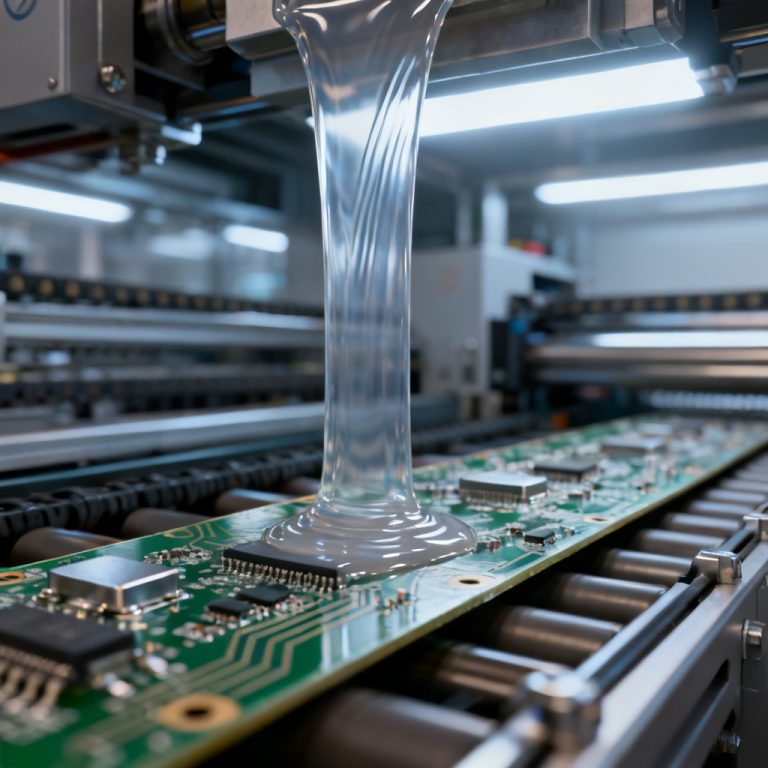
An Assembly Process Overview SMT Through Hole Mixed and SMT begins with solder paste printing. A stainless steel stencil is aligned precisely over the bare PCB. Solder paste—a mixture of tiny solder spheres and flux—is applied and spread across the stencil using a metal squeegee blade.
Critical parameters include stencil thickness (typically 100–150 µm), aperture size, and squeegee pressure. Paste viscosity is temperature and humidity sensitive. Post-printing, Automated Optical Inspection (AOI) checks for paste volume, height, and alignment. Insufficient paste leads to open joints; excess paste causes solder bridges.
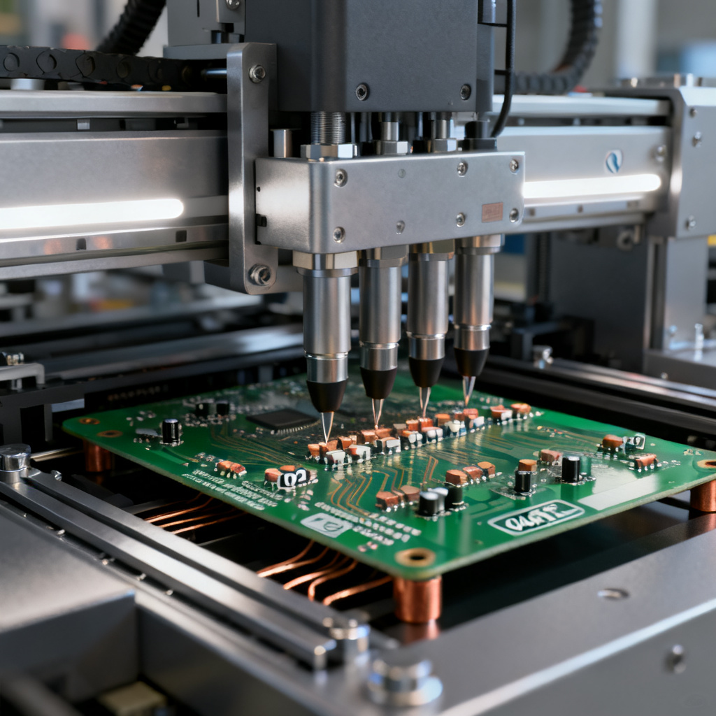
Next, high-speed pick-and-place machines use vacuum nozzles to retrieve components from tape-and-reel, tray, or tube feeders. Vision systems align component leads to PCB pads. Components are placed with high precision (typically ±40–50 µm). For ultra-fine pitch components (e.g., 0.4mm BGA), advanced 3D vision systems are used. Key considerations include component orientation (polarity), centering, and force control. Incorrect placement leads to tombstoning or misalignment during reflow.
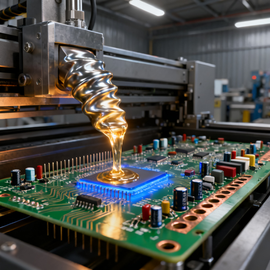
Reflow soldering follows, where the board passes through a multi-zone reflow oven with a controlled thermal profile. The profile includes four phases: preheat (slow ramp-up to activate flux), soak (even temperature distribution), reflow (peak temperature above solder melting point, e.g., 245°C for SAC305), and cooling (rapid solidification). A nitrogen atmosphere reduces oxidation and improves wetting, especially for lead-free solders. A proper profile prevents cold joints, head-in-pillow, and component damage from thermal shock.
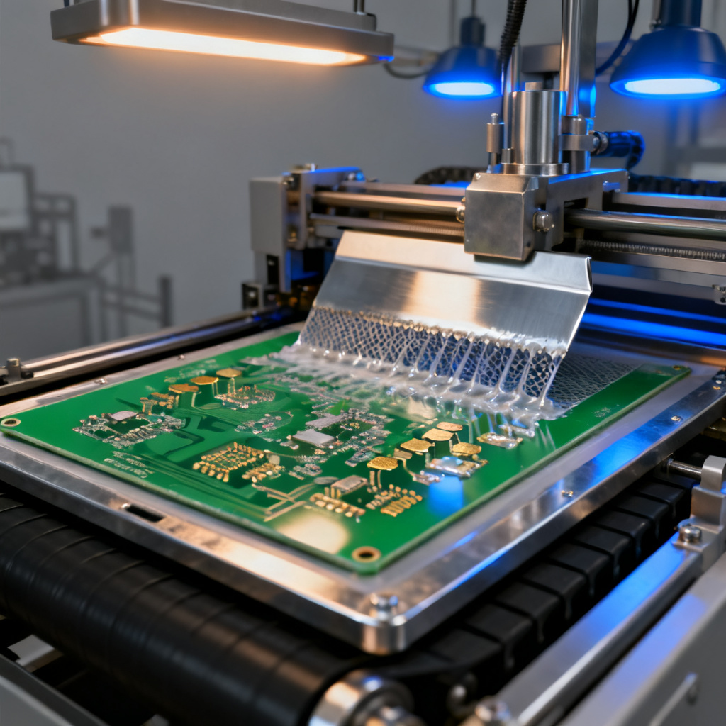
Cleaning is optional but recommended for high-reliability applications. For no-clean flux, cleaning may be skipped. However, for medical devices, aqueous or solvent cleaning removes flux residues that can cause electromigration or corrosion. Methods include ultrasonic, spray-in-air, or batch cleaning systems.
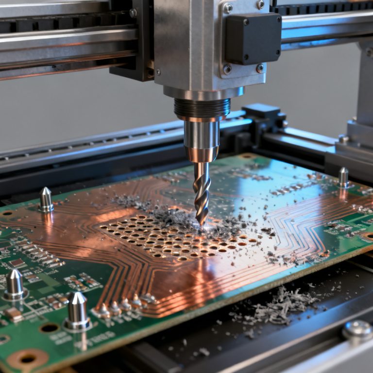
Inspection and testing include AOI, which checks for missing, misaligned, or tombstoned components and solder joint quality. Automated X-ray Inspection (AXI) is essential for BGA, QFN, and other hidden solder joints, revealing voids, bridges, and insufficient solder. In-Circuit Test (ICT) uses bed-of-nails fixtures to test individual components (resistance, capacitance, diode drops) and opens/shorts. Flying Probe Test is used for low-volume or prototype runs without a custom fixture.
Through-Hole Technology (THT) Assembly Process Overview
This assembly process overview for THT starts with component preparation and insertion. Components (e.g., connectors, transformers, large capacitors, relays) are manually or automatically inserted. Axial components are formed (bent) to fit the hole pitch. For high volume, radial or axial insertion machines handle components. Manual insertion is used for odd-form or low-volume jobs. Critical checks include verifying correct orientation (polarity for diodes, capacitors) and full seating of leads through the board.
Wave soldering is the primary method. The board passes over a wave of molten solder (typically 260°C for lead-free). A fluxer applies flux to the bottom side, preheaters warm the board, and then the board contacts the solder wave. Dual-wave systems (turbulent wave + laminar wave) improve wetting and reduce bridging.
The turbulent wave penetrates tight spaces; the laminar wave removes excess solder. Selective soldering is used for mixed-technology boards where SMT components are already on the bottom, using a localized mini-wave or laser to solder only THT leads.
Hand soldering is an alternative for prototypes, repairs, or low-volume work. Skilled operators use soldering irons (typically 350–400°C) with fine tips. Best practices include using flux-cored solder, clean tips, and proper dwell time (2–4 seconds) to avoid pad lifting or component damage.
Inspection and testing include visual inspection for solder bridges, insufficient solder, cold joints, and disturbed joints. A pull test measures the force required to separate the lead from the pad for critical joints. ICT test pins contact the THT leads or pads.
Mixed Technology Assembly Process Overview
Mixed Technology boards combine SMT components (for density) with THT components (for robustness or high power). This assembly process overview requires careful process sequencing. Option A (SMT-first): solder paste printing → SMT placement → Reflow → (Optional: flip board) → THT insertion → Wave soldering (or selective soldering). Option B (THT-first): THT insertion → Wave soldering → (Optional: clean) → SMT placement on bottom side → Reflow (if bottom-side SMT). Option C (Glue-based): apply glue to bottom-side SMT pads → Place SMT components → Cure glue → Insert THT components → Wave solder (both SMT and THT in one pass).
Key challenges include thermal management (reflow can damage THT components like connectors with plastic housings). Solution: use high-temperature THT components or use selective soldering after reflow. Solder bridges can occur when wave soldering over SMT pads on the bottom side. Solution: use solder mask dams or dedicated wave solder pallets that shield SMT areas. Flux residue from wave soldering may leave residues under SMT components. Solution: use low-spatter flux or post-assembly cleaning.
Inspection for mixed technology uses combined AOI/AXI: AOI for visible SMT and THT joints; AXI for hidden BGA/QFN and THT barrel fill. ICT with mixed fixtures must accommodate both SMT pads and THT leads.
Quality Assurance and Reliability Considerations
Regardless of the method, this assembly process overview emphasizes Design for Assembly (DFA). For SMT, avoid fine-pitch components near board edges, provide adequate pad-to-pad spacing, and use fiducial marks for alignment. For THT, ensure hole-to-lead diameter ratio (typically 1.5:1 to 2:1) and avoid tight hole spacing for wave soldering. For mixed, place THT components away from SMT areas to allow selective soldering pallets.
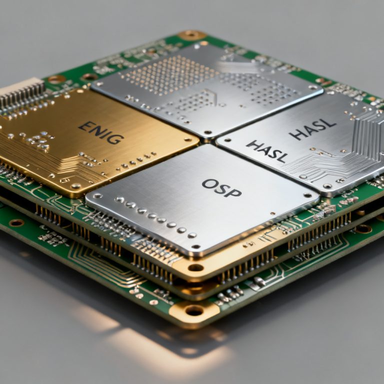
Solder alloy selection is critical. Lead-free (e.g., SAC305, SAC405) is mandatory for RoHS compliance, with higher melting point (217–220°C) requiring higher reflow temperatures and nitrogen atmosphere. Lead-based (e.g., Sn63Pb37) offers excellent wetting and reliability, used for military, aerospace, and medical where RoHS exemptions apply.
Process control and monitoring include Statistical Process Control (SPC) to monitor paste volume, placement accuracy, reflow profile, and wave height. First Article Inspection (FAI) is performed for every new design to verify component placement, polarity, and solder quality.
Environmental and reliability testing includes thermal cycling (expose assembled boards to -40°C to +125°C cycles to check for solder joint cracking), vibration testing (simulates shipping and operational conditions), and contamination testing (ionic cleanliness testing per IPC-TM-650 ensures no corrosive residues).
Key Assembly Process Parameters Table
| Parameter | SMT Assembly | THT Assembly | Mixed Technology |
|---|---|---|---|
| Component Density | High | Low to Medium | Medium to High |
| Mechanical Strength | Moderate | High | High (THT areas) |
| Typical Soldering Temp | 245°C (SAC305) | 260°C (lead-free) | Varies (reflow + wave) |
| Primary Inspection Method | AOI + AXI | Visual + Pull Test | Combined AOI/AXI |
| Best For | High-volume, dense designs | High-power, rugged applications | Complex systems with mixed requirements |
Frequently Asked Questions (FAQ)
What is the main difference between SMT and Through-Hole in an assembly process overview?
In an assembly process overview, SMT mounts components directly on the PCB surface, enabling higher density and automation, while THT inserts leads through holes for superior mechanical strength and power handling.
How do I choose between SMT, THT, and Mixed Technology for my PCB assembly?
Your assembly process overview choice depends on product needs: use SMT for high-density consumer devices, THT for rugged industrial applications, and Mixed Technology for complex systems requiring both density and robustness.
What are common defects in the assembly process overview for Mixed Technology?
Common defects in a Mixed Technology assembly process overview include solder bridges from wave soldering over SMT pads, thermal damage to THT components during reflow, and flux residue under SMT components.
Why is nitrogen atmosphere used in reflow soldering?
In the assembly process overview, nitrogen atmosphere reduces oxidation and improves wetting, especially for lead-free solders, leading to better solder joint quality and higher yields.
What is the role of AXI in PCB assembly inspection?
Automated X-ray Inspection (AXI) in an assembly process overview is essential for detecting hidden defects in BGA, QFN, and THT barrel fill, such as voids, bridges, and insufficient solder.