Complete PCB Manufacturing Process: From Inner Layer to Finished Board
The complete PCB manufacturing process from inner layer to finished board is the foundation of reliable electronics. Understanding every stage—from material selection to final inspection—enables B2B buyers to evaluate suppliers, optimize designs, and ensure quality. This guide covers the entire journey of a printed circuit board, including lamination, drilling, plating, and testing, to help you make informed procurement decisions.
1. Step-by-Step Complete PCB Manufacturing Process From Inner Layer to Finished Board
1.1 Material Selection and Cutting for the PCB Manufacturing Process
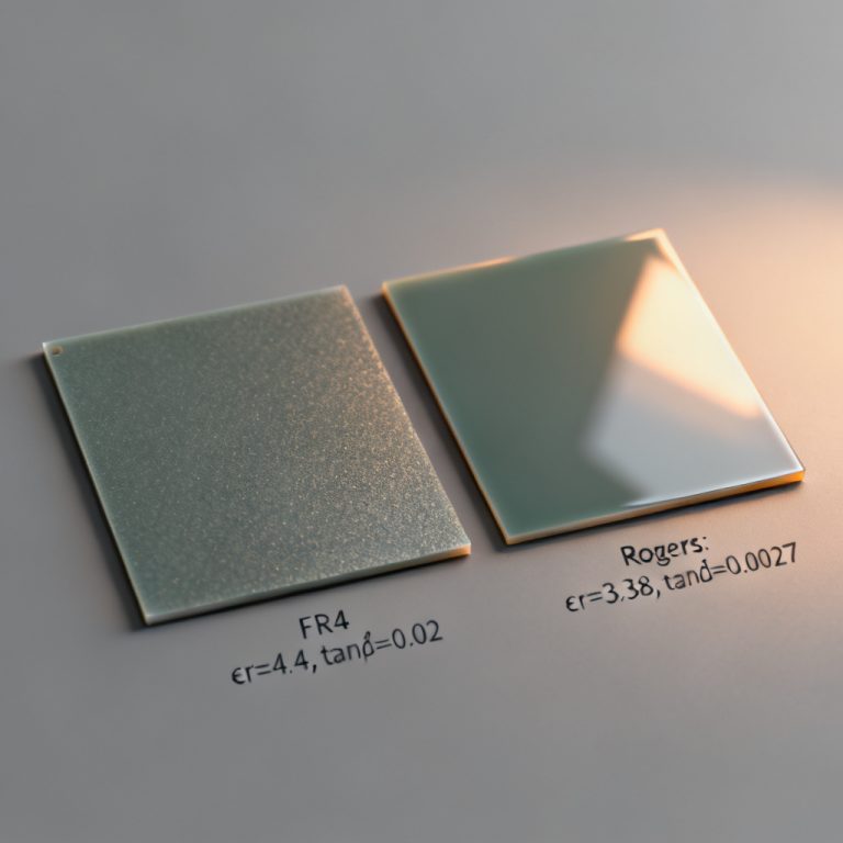
The PCB manufacturing process begins with selecting a copper-clad laminate (CCL), typically FR-4 for standard applications or high-frequency materials like Rogers for RF circuits. The raw laminate is cut into panels using a CNC router or shear cutter, sized to match final dimensions with handling allowances. High-end manufacturers use automated optical inspection (AOI) to verify material thickness and copper uniformity before processing. Copper thickness is measured in ounces per square foot (e.g., 1 oz = 35 µm), with tolerances of ±10% for standard designs.
1.2 Inner Layer Imaging and Photoresist Application
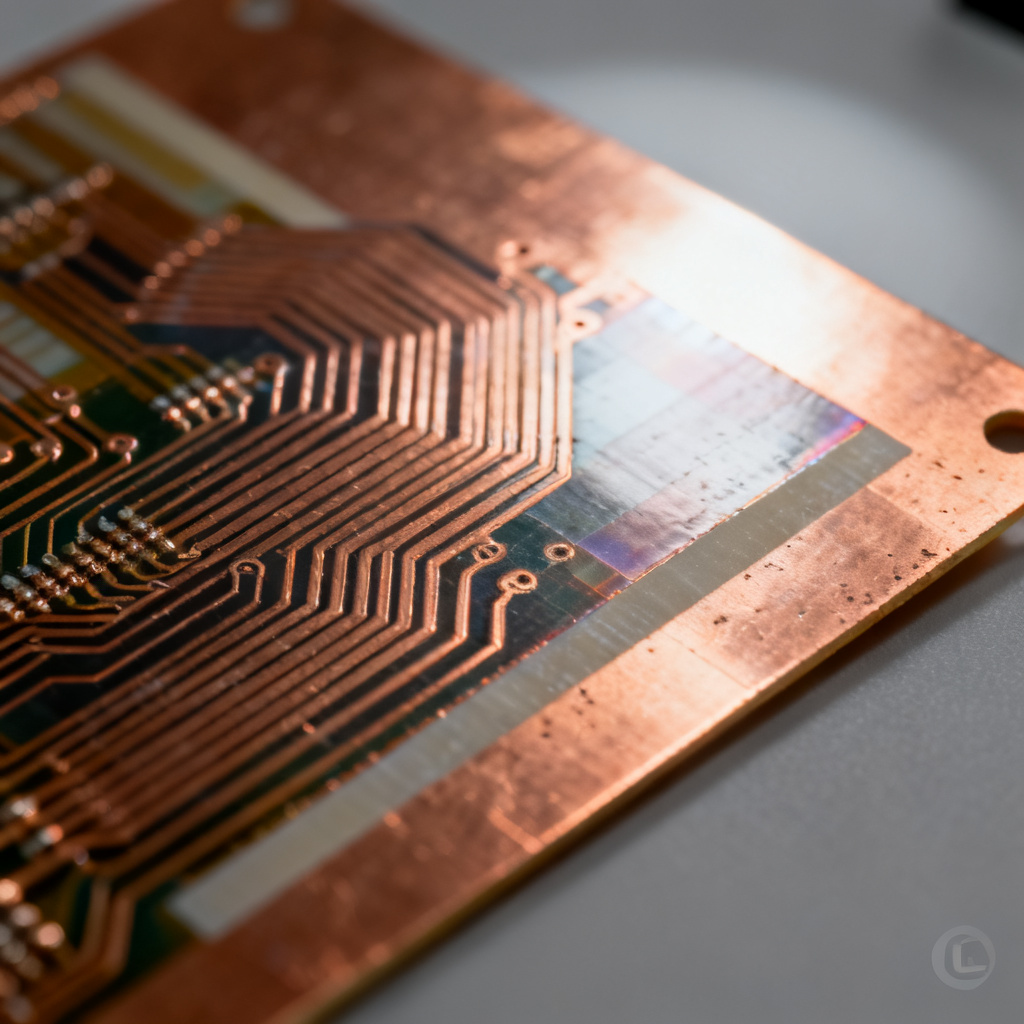
A photosensitive dry film (photoresist) is laminated onto the clean copper surface using a hot-roll laminator. The board is exposed to UV light through a phototool—a film negative of the circuit pattern. UV hardens the photoresist in areas corresponding to desired copper traces, while unexposed areas remain soluble. For high-density interconnect (HDI) boards, laser direct imaging (LDI) replaces phototools, offering higher resolution down to 25 µm line/space and eliminating film alignment errors.
1.3 Developing and Etching in the PCB Manufacturing Process
The panel passes through a developer solution (typically sodium carbonate) to remove unexposed photoresist, revealing copper to be etched. Etching uses an alkaline or acidic solution (e.g., cupric chloride or ammonium persulfate) to dissolve unprotected copper, leaving only hardened photoresist-covered traces. Etching parameters—temperature, conveyor speed, and solution concentration—are monitored in real-time using pH and conductivity sensors. Post-etch, the photoresist is stripped using a caustic solution (e.g., sodium hydroxide), leaving bare copper traces.
1.4 Automated Optical Inspection (AOI) for Inner Layers
After etching, each inner layer undergoes AOI using high-resolution cameras to detect defects like shorts, opens, nicks, or pinholes. AOI systems compare the actual pattern to original CAD data (Gerber files). Defective panels are flagged for rework or scrapped. AOI systems can detect copper nodules as small as 10 µm. For critical applications (e.g., aerospace), manual inspection under a microscope supplements AOI.
1.5 Oxide Treatment (Black Oxide or Brown Oxide)
To enhance adhesion between the inner layer and prepreg during lamination, the copper surface is chemically treated with an oxide coating. Black oxide (using sodium chlorite) creates a roughened, dark surface, while brown oxide (using alternative chemistries) offers better thermal stability. This step prevents delamination under thermal stress.
2. Layer Lamination – Bonding the Stack-Up in the PCB Manufacturing Process
2.1 Prepreg and Core Stacking
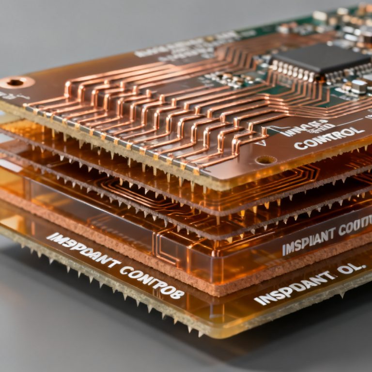
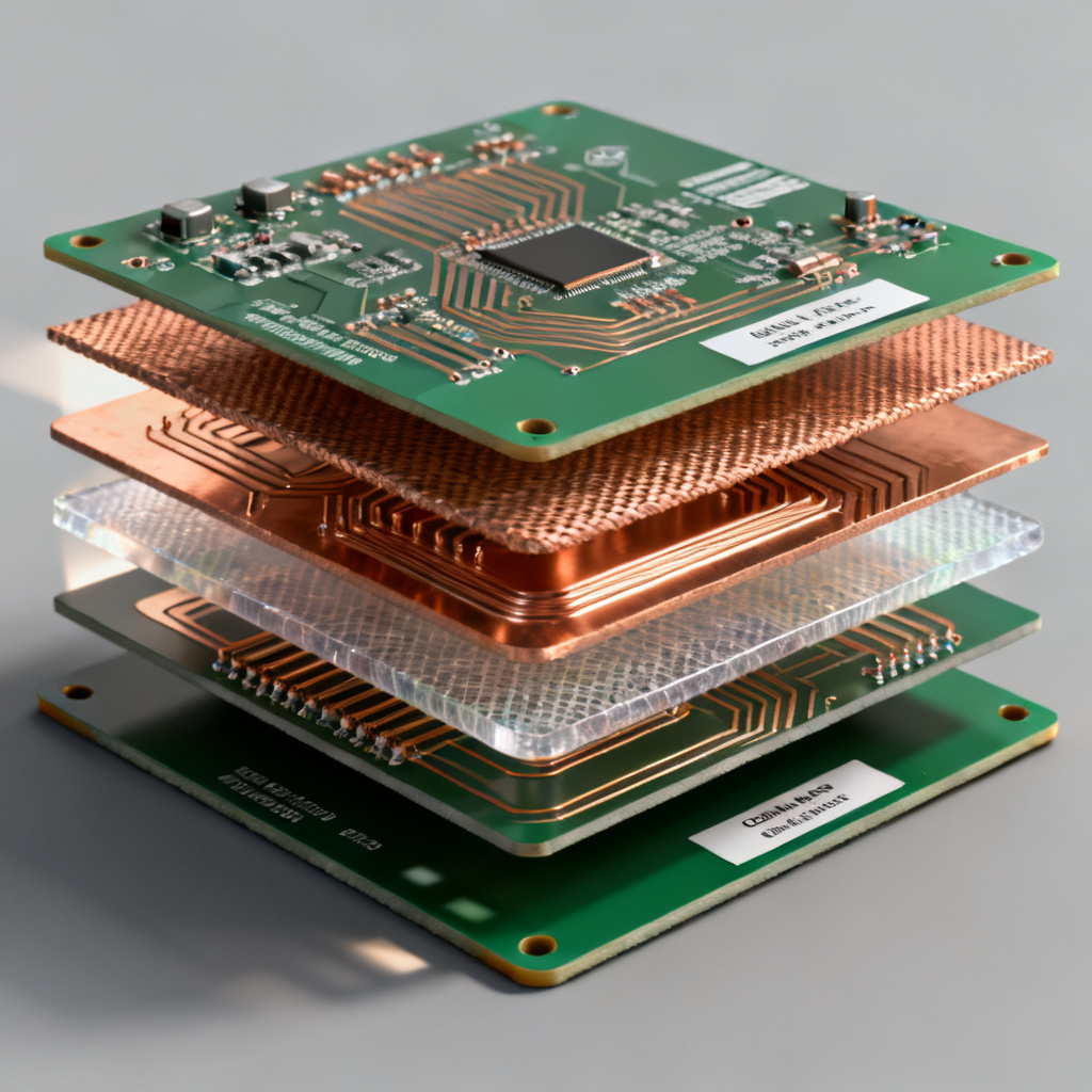
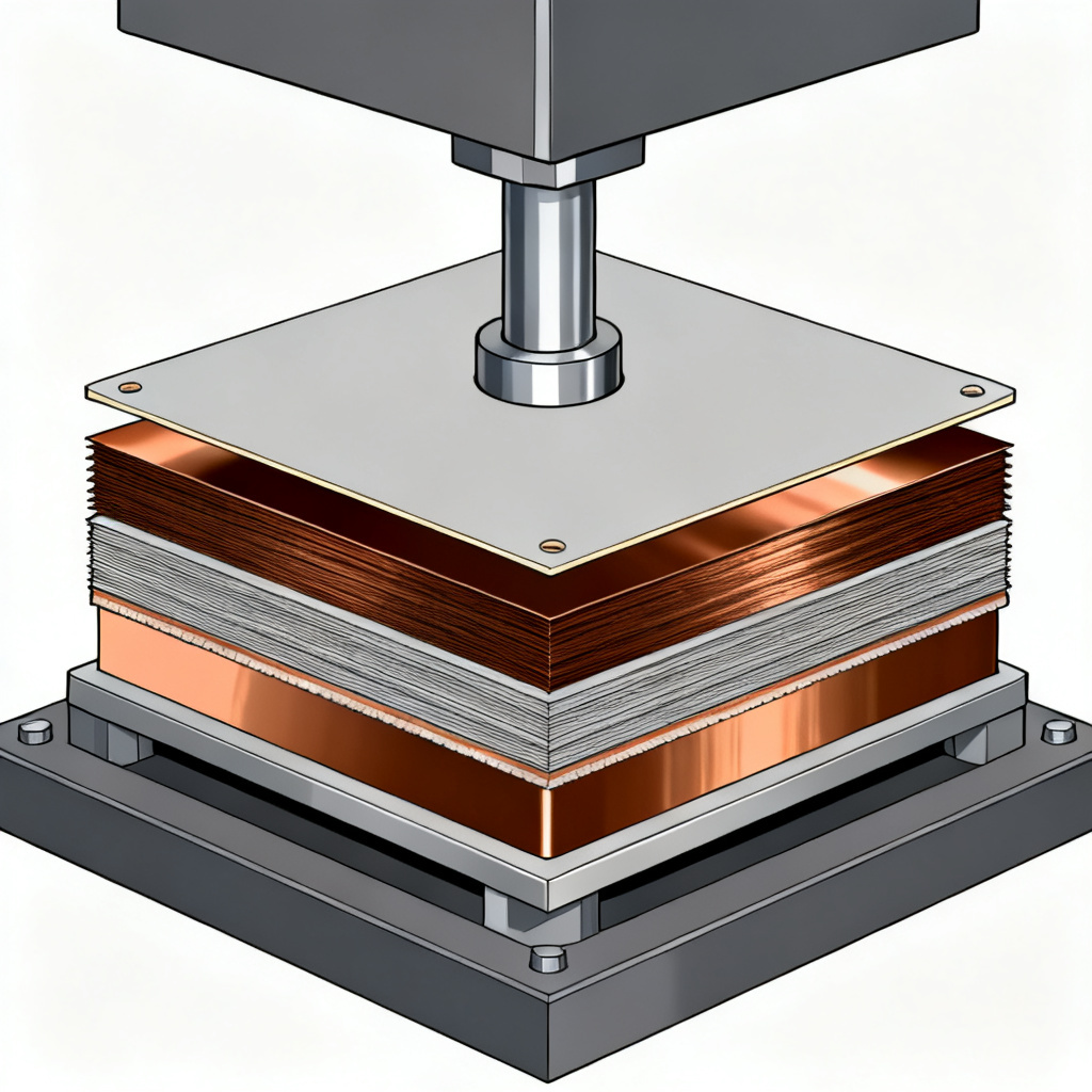
The inner layers are stacked with sheets of prepreg (pre-impregnated fiberglass cloth with partially cured epoxy) and copper foil for outer layers. The stack-up is placed in a hydraulic press with precise alignment using tooling pins or an optical registration system. A typical multi-layer stack might include: copper foil, prepreg, inner layer core, prepreg, and another copper foil. For controlled impedance designs, the dielectric thickness between layers is critical. Manufacturers use prepreg with specific resin content (e.g., 50% to 65%) to achieve target impedance values (e.g., 50 Ω or 100 Ω differential).
2.2 Pressing and Curing
The stack is subjected to high temperature (170°C to 190°C) and pressure (300 to 500 psi) for 1 to 2 hours, causing the prepreg resin to flow, fill gaps, and cure into a solid insulating layer. The pressure ensures uniform bonding and eliminates voids. Vacuum lamination is used to remove trapped air and moisture, which can cause blistering or delamination. The press cycle includes a ramp-up phase (gradual temperature increase) to prevent thermal shock.
2.3 Post-Lamination Inspection
After cooling, the laminated panel is inspected for thickness uniformity, warpage, and visual defects. X-ray inspection may be used to verify inner layer alignment (registration) by checking target marks (fiducials).
3. Drilling – Creating Interconnections in the PCB Manufacturing Process
3.1 CNC Drilling
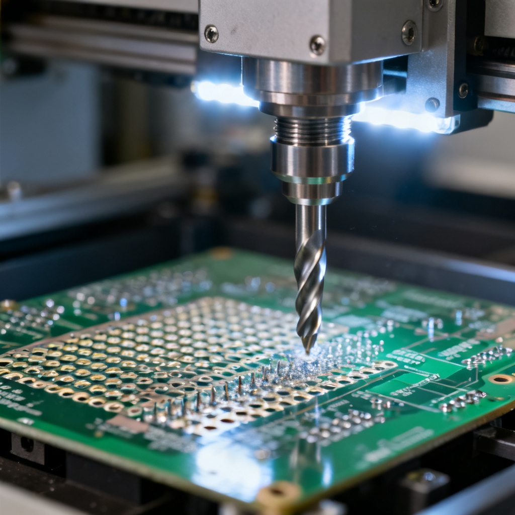
A CNC drilling machine with high-speed spindles (up to 300,000 RPM) drills holes for through-hole components, vias, and mounting holes. Drill bits are typically tungsten carbide, with diameters ranging from 0.2 mm (8 mils) to 6.35 mm (250 mils). The drilling pattern is programmed from the design’s NC drill file. For HDI boards, laser drilling (CO₂ or UV) creates microvias (diameters less than 150 µm) with high aspect ratios. Laser drilling is faster and more precise for small vias.
3.2 Deburring and Cleaning
Drilling leaves burrs and resin smear on hole walls. The panel is deburred using a mechanical brush or high-pressure water jet, followed by chemical cleaning (e.g., with sulfuric acid) to remove residual epoxy and prepare the surface for plating. Plasma cleaning (using oxygen or argon plasma) is employed for advanced boards to remove organic contaminants without damaging copper.
3.3 Desmear (Etchback)
For multi-layer boards, drilling can smear epoxy over inner layer copper pads. A desmear process (using permanganate or plasma) removes this smear, exposing clean copper for reliable electrical connections. Etchback (controlled removal of resin) further ensures via reliability.
4. Plating – Conductive Through-Holes in the PCB Manufacturing Process
4.1 Electroless Copper Deposition
The panel is immersed in a series of chemical baths to deposit a thin layer of copper (0.5 to 1 µm) on the hole walls. This process uses palladium catalyst and formaldehyde-based reduction to initiate copper deposition. Electroless copper makes the holes conductive for subsequent electroplating. The electroless copper bath is continuously filtered and analyzed for copper concentration (typically 1.5 to 3 g/L) and temperature (25°C to 30°C) to ensure uniform deposition.
4.2 Panel Plating (Flash Plating)
A thin layer of copper (5 to 8 µm) is electroplated onto the entire panel surface and hole walls to build up thickness. The panel is connected to a cathode, and copper anodes dissolve in a sulfuric acid/copper sulfate solution. Current density (10 to 30 A/ft²) is carefully regulated.
4.3 Pattern Plating (Selective Plating)
For finer control, a photoresist is applied again to protect non-conductive areas. The exposed copper (traces and pads) is electroplated with additional copper (typically 25 to 50 µm) to achieve final thickness. This is followed by tin or tin-lead plating as an etch resist for outer layer etching. Pattern plating allows for differential copper thickness (e.g., 1 oz on outer layers, 0.5 oz on inner layers) to meet current-carrying requirements.
5. Outer Layer Imaging and Etching in the PCB Manufacturing Process
5.1 Photoresist Application and Exposure
Similar to inner layers, a photoresist is applied to the outer layers. The panel is exposed using a phototool or LDI, aligning the pattern to existing features (via targets). The photoresist is developed to expose copper areas to be etched.
5.2 Etching and Stripping
The outer layer copper is etched using an alkaline etchant (e.g., ammonia-based) that removes copper but does not attack the tin or tin-lead plating. After etching, the tin resist is stripped using nitric acid or a proprietary stripper, leaving the final copper pattern. For fine-pitch BGA pads, a two-step etching process (coarse then fine) is used to minimize undercut and maintain pad geometry.
6. Solder Mask Application in the PCB Manufacturing Process
6.1 Cleaning and Pre-Treatment
The panel is cleaned to remove residues. A chemical micro-etch (e.g., using sodium persulfate) roughens the copper surface for better solder mask adhesion.
6.2 Solder Mask Application Methods
Liquid Photoimageable Solder Mask (LPSM): A liquid mask is curtain-coated or screen-printed onto the panel, then exposed to UV through a phototool. Unexposed areas are developed away, revealing pads and vias. Dry Film Solder Mask: A dry film is laminated onto the panel, exposed, and developed. This method is preferred for fine-pitch designs due to better resolution. Solder mask thickness is typically 0.5 to 1 mil (12.5 to 25 µm). For high-voltage applications, thicker masks (2 mil) are used to prevent arcing.
6.3 Curing
The solder mask is cured in a thermal oven or UV conveyor to achieve chemical and mechanical resistance. Typical curing cycles range from 30 minutes at 150°C to 1 hour at 100°C.
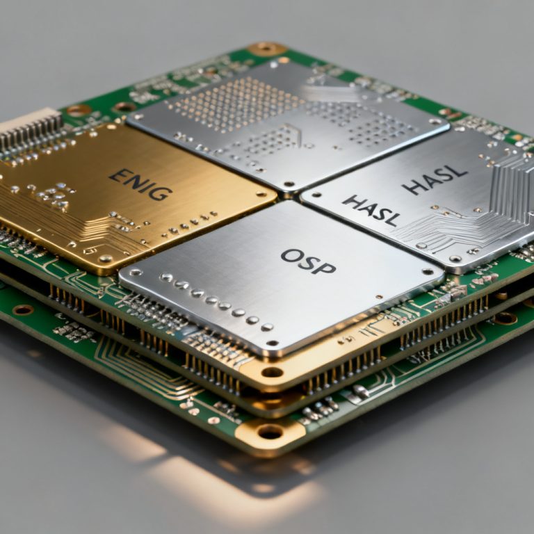
7. Surface Finish – Protecting Exposed Copper in the PCB Manufacturing Process
Exposed copper pads must be protected from oxidation to ensure solderability. Common finishes include:
- HASL (Hot Air Solder Leveling): The board is dipped in molten solder (Sn/Pb or lead-free), and excess is blown off with hot air. This is cost-effective but results in uneven surfaces (not suitable for fine-pitch components).
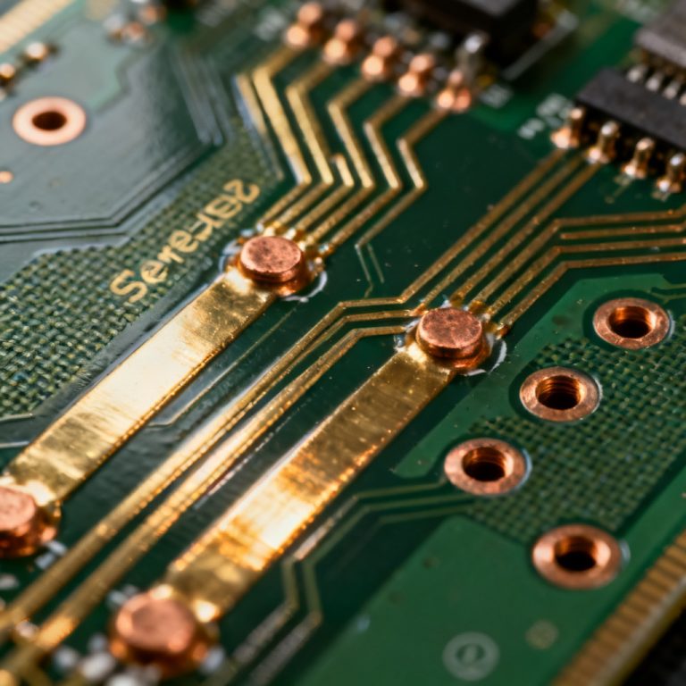
- ENIG (Electroless Nickel Immersion Gold): A nickel layer (3-6 µm) is deposited, followed by a thin gold layer (0.05-0.15 µm). ENIG offers flat surfaces and excellent corrosion resistance, ideal for BGA and QFN packages.
- OSP (Organic Solderability Preservative): A water-based organic compound is applied to copper, protecting it until soldering. OSP is eco-friendly but has limited shelf life (6-12 months).
- Immersion Silver and Immersion Tin: These finishes provide flat surfaces and are used for specific applications (e.g., silver for RF, tin for low-cost).
ENIG is prone to “black pad” defects (nickel corrosion) if process parameters are not controlled. Manufacturers use X-ray fluorescence (XRF) to verify gold thickness and nickel purity. For high-reliability applications (e.g., automotive), ENEPIG (Electroless Nickel Electroless Palladium Immersion Gold) is used, adding a palladium layer to prevent nickel migration.
8. Electrical Testing – Ensuring Functionality in the PCB Manufacturing Process
8.1 Flying Probe Testing
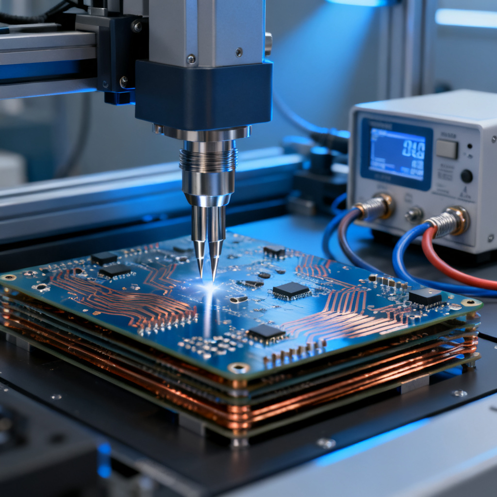
A flying probe tester uses moving probes to contact each net on the board, checking for shorts, opens, and resistance values. This is ideal for prototypes and low-volume runs (no fixture required).
8.2 Fixture-Based Testing (Bed-of-Nails)
For high-volume production, a custom fixture with spring-loaded pins contacts all test points simultaneously. This method is faster but requires a dedicated fixture (costly for small runs).
8.3 Impedance Testing (TDR)
For high-speed designs, time-domain reflectometry (TDR) measures characteristic impedance (e.g., 50 Ω ±10%). This ensures signal integrity for RF and digital circuits. Testing parameters include insulation resistance (typically >100 MΩ at 500V) and continuity (resistance <5 Ω for standard traces). High-voltage testing (e.g., 1000V) is performed for power PCBs.
9. Final Inspection and Quality Assurance in the PCB Manufacturing Process
9.1 Visual and Dimensional Inspection
Technicians inspect boards for cosmetic defects (scratches, discoloration, solder mask voids). Dimensional checks verify hole diameters, pad sizes, and overall board dimensions using optical comparators or CMM (Coordinate Measuring Machine).
9.2 Solderability Testing
A sample board is fluxed and dipped in molten solder to assess wetting and capillary action. This is critical for ensuring reliable assembly.
9.3 Thermal Stress Testing
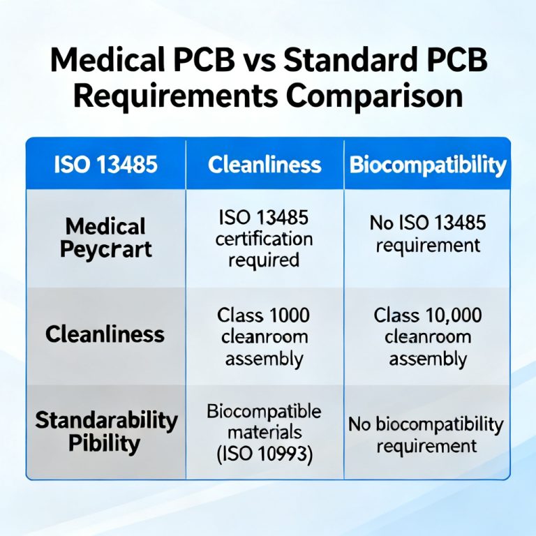
Boards are subjected to thermal shock (e.g., -40°C to +125°C) or reflow simulation (260°C peak) to check for delamination, blistering, or micro-cracks. IPC standards (e.g., IPC-6012) define acceptance criteria. Cross-sectioning is performed on a sample board to measure copper thickness, plating integrity, and resin fill in vias. This destructive test provides quantitative data. For military or medical applications, 100% X-ray inspection of inner layers and vias is mandatory to detect hidden defects.
10. Packaging and Shipment in the PCB Manufacturing Process
10.1 Cleaning and Drying
The final boards are cleaned to remove flux residues, dust, and fingerprints. Vacuum drying ensures no moisture remains (to prevent corrosion during storage).
10.2 Packaging
Boards are stacked with interleaving paper or plastic sheets to prevent scratching. For moisture-sensitive finishes (e.g., OSP), vacuum-sealed bags with desiccant and humidity indicators are used. Shipment is typically in ESD-safe packaging. For large orders, manufacturers provide a Certificate of Conformance (CoC) and a packing list detailing batch numbers, quantities, and test results.
Frequently Asked Questions About the PCB Manufacturing Process
What is the first step in the PCB manufacturing process?
How long does the complete PCB manufacturing process take?
What quality checks are performed in the PCB manufacturing process?
PCB Manufacturing Process Specifications Table
| Process Stage | Key Parameter | Typical Value in PCB Manufacturing Process |
|---|---|---|
| Inner Layer Etching | Copper thickness | 1 oz (35 µm) ±10% |
| Lamination | Temperature | 170°C – 190°C |
| Drilling | Minimum hole diameter | 0.2 mm (8 mils) |
| Plating | Electroless copper thickness | 0.5 – 1 µm |
| Solder Mask | Thickness | 0.5 – 1 mil (12.5 – 25 µm) |
| Electrical Testing | Insulation resistance | >100 MΩ at 500V |
Glossary of PCB Manufacturing Terms
- Prepreg: Pre-impregnated fiberglass cloth with partially cured epoxy, used as an insulating layer between cores in the PCB manufacturing process.
- Desmear: A chemical or plasma process to remove epoxy smear from drilled hole walls, ensuring reliable copper plating in the PCB manufacturing process.
- Microvia: A small via (less than 150 µm diameter) created by laser drilling, common in HDI boards within the PCB manufacturing process.
- ENIG: Electroless Nickel Immersion Gold, a surface finish that protects copper pads and ensures solderability in the PCB manufacturing process.
Comparison: Our PCB Manufacturing Process vs. Industry Standards
Our PCB manufacturing process adheres to IPC Class 2 and Class 3 standards, with additional quality checks such as 100% AOI for inner layers and X-ray inspection for multi-layer alignment. Unlike many suppliers, we offer free DFM feedback and real-time process monitoring, ensuring higher yield rates and faster turnaround times.