Dielectric Loss and Dispersion in High Speed PCBs
Dielectric Loss and Dispersion in High-Speed PCBs: The Ultimate Guide to Material Selection and Signal Integrity
Dielectric Loss and Dispersion in High Speed PCBs are the dominant factors degrading signal integrity at multi-gigabit data rates. This guide synthesizes expert insights from leading engineering sources to help you master material selection, measurement, and mitigation strategies for optimal performance.
Understanding Dielectric Loss and Dispersion in High-Speed PCBs
The Dissipation Factor (Df) and Loss Tangent
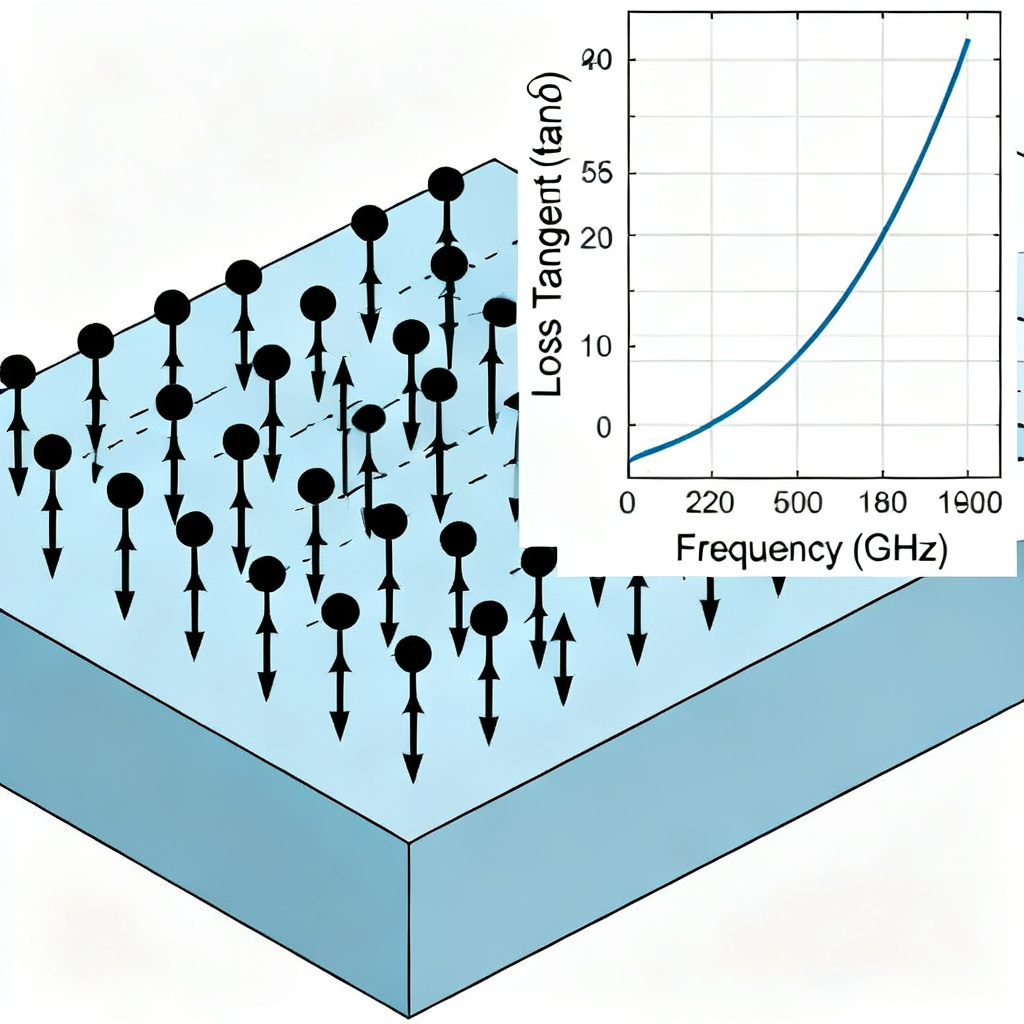
Dielectric loss and dispersion begin with the dissipation factor (Df), also known as loss tangent (tan δ). Df quantifies the inefficiency of a dielectric material as the ratio of its imaginary permittivity (ε”) to real permittivity (ε’): tan δ = ε”/ε”. The real part (ε’) is the dielectric constant (Dk) governing signal velocity; the imaginary part (ε”) represents energy lost to dipole friction and conduction. When an electric field passes through a dielectric, polar molecules in epoxy resins attempt to align with the field. At high frequencies, these molecules cannot keep up, causing internal friction that converts electrical energy into heat—this is the dominant loss mechanism in most PCB laminates. Critically, Df is not a constant; it typically increases with frequency. Standard FR-4 might have Df of 0.02 at 1 GHz but rise to 0.03 or higher at 10 GHz. Low-loss materials like Rogers 4350B or Isola I-Tera MT40 show a much flatter Df curve, making them essential for high-speed designs.
The Role of Moisture Absorption
A factor often overlooked is moisture absorption’s impact on dielectric loss and dispersion. Water has a very high Df (~0.1) and high Dk (~80). When a PCB laminate absorbs moisture, water molecules act as highly lossy dipoles, increasing both Dk (slowing signals) and Df (increasing loss). This is particularly problematic for materials with high moisture absorption rates, such as standard FR-4. High-speed laminates are engineered with hydrophobic resins (e.g., modified epoxy, polyphenylene ether, or PTFE) to minimize moisture uptake. Always check the “Moisture Absorption” spec (e.g., IPC-TM-650 2.6.2.1) when selecting materials. A material with less than 0.1% moisture absorption is generally preferred for high-speed applications.
Dispersion in High-Speed PCBs: The Frequency-Dependent Dk
What is Dispersion and Why Does It Matter?
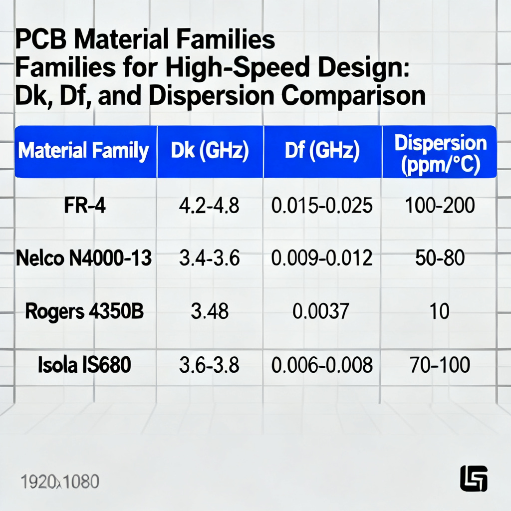
Dielectric loss and dispersion include the variation of Dk with frequency, a primary cause of signal degradation. The same dipole relaxation mechanism that causes loss also causes Dk to change. At low frequencies, dipoles have time to fully align, resulting in a higher effective Dk. At high frequencies, dipoles cannot keep up, and the effective Dk decreases. This transition region is the source of dispersion. A square wave (like a clock signal) is composed of a fundamental frequency and many higher-order harmonics. If Dk differs for each harmonic, each component travels at a different velocity, causing pulse broadening and inter-symbol interference (ISI). Advanced sources define dispersion as ΔDk = Dk(1 MHz) – Dk(10 GHz). For standard FR-4, ΔDk can be as high as 0.2 to 0.3. For low-dispersion materials (e.g., PTFE-based or advanced hydrocarbon ceramics), ΔDk is typically less than 0.05.
The Glass Weave Effect: A Practical Dispersion Pitfall
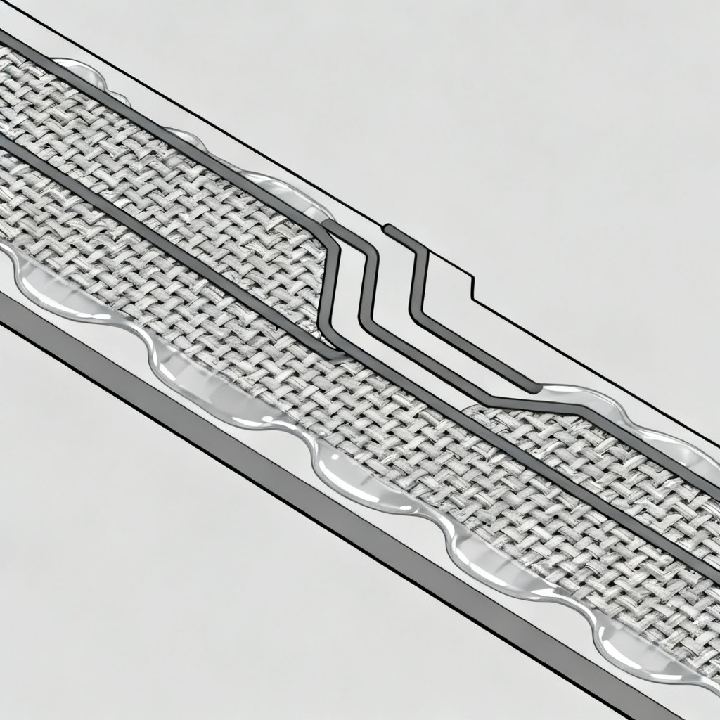
A practical source of effective dispersion is the glass weave effect—not a material property but a construction artifact. Woven glass fabric has a higher Dk (~6) than pure resin (~3), creating a non-uniform dielectric environment. As a signal trace runs across the board, it sometimes lies over a bundle of glass fibers (high Dk) and sometimes over a resin-rich area (low Dk). This creates skew between different traces in a differential pair or bus, causing timing mismatches. Solutions include using spread glass (or open weave) fabrics for more uniform Dk distribution, resin-coated copper (RCC) foils that eliminate the glass weave near the trace, and routing traces at an angle (e.g., 10–15 degrees) to average out the effect.
The Interplay of Conductor Loss and Dielectric Loss in High-Speed PCBs
The Total Loss Equation
Total insertion loss in a PCB trace is α_total = α_c + α_d. Conductor loss (α_c) is dominated by skin effect at high frequencies, scaling with √f and inversely with trace width and copper thickness. Dielectric loss (α_d) is dominated by the dissipation factor, scaling linearly with frequency and √Dk. At frequencies below ~1 GHz, conductor loss typically dominates. Above ~3–5 GHz, dielectric loss and dispersion become the dominant factor, often accounting for 70–80% of total loss at 10 Gbps+.
Copper Surface Roughness: A Hidden Contributor
Copper surface roughness increases the path length for current flow (due to skin effect) and creates micro-capacitors and micro-inductors at the interface, effectively increasing conductor loss and modifying effective Dk and Df. The roughness factor can increase conductor loss by 20–50% at 10 GHz compared to a perfectly smooth surface. High-frequency laminates often use very low profile (VLP) or reverse-treated copper (RTF) foils with bonding surfaces less than 2 µm roughness, compared to 5–10 µm for standard HTE copper.
Material Selection Strategy for Low Dielectric Loss and Dispersion
Material Families and Their Performance
| Material Family | Typical Dk (10 GHz) | Typical Df (10 GHz) | Dispersion (ΔDk) | Moisture Absorption | Cost | Best For |
|---|---|---|---|---|---|---|
| Standard FR-4 (e.g., 370HR) | 4.2–4.5 | 0.020–0.025 | High (>0.2) | High (0.2–0.3%) | Low | < 1 Gbps, low-cost designs |
| Mid-Range / Modified Epoxy (e.g., Isola 370HR, Nelco 4000-13) | 3.8–4.2 | 0.010–0.015 | Moderate (0.1–0.15) | Moderate (0.1–0.2%) | Medium | 1–5 Gbps, cost-sensitive high-speed |
| High-Speed / Low-Loss (e.g., Isola I-Tera MT40, Rogers 4350B, Panasonic Megtron 6) | 3.4–3.7 | 0.002–0.005 | Low (<0.05) | Low (<0.1%) | High | 10–25 Gbps, SERDES, RF |
| Ultra-Low Loss (e.g., Rogers 3003/5880, Taconic RF-35, PTFE-based) | 2.2–3.0 | 0.0009–0.002 | Very Low (<0.02) | Very Low (<0.02%) | Very High | > 25 Gbps, mmWave, high-reliability RF |
Key Specifications to Request from Your Supplier
When specifying a PCB laminate for a high-speed design, ask for Dk and Df at the design frequency (not just 1 GHz data for a 10 GHz design), Dk and Df stability over temperature (TCDk and TCDf), Dk and Df tolerance for impedance control, and glass weave style (specify spread glass for fine-pitch differential pairs).
Measurement and Modeling Best Practices for Dielectric Loss and Dispersion
How to Measure Dielectric Loss and Dispersion Accurately
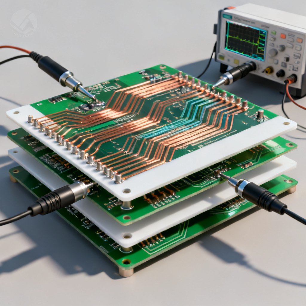
Accurate measurement is essential. The stripline resonator method is the gold standard for measuring Dk and Df, using a resonant cavity created with the material under test. For simulation, use 3D EM simulators (e.g., Ansys HFSS, CST Studio) with Debye or Djordjevic-Sarkar models that capture frequency-dependent Dk and Df. Time Domain Reflectometry (TDR) can reveal dispersion—a dispersive line shows characteristic “smearing” of the reflected pulse edge, while a clean sharp edge indicates low dispersion.
Modeling Surface Roughness in Simulations
A common mistake is ignoring copper roughness. The Huray model is the most widely accepted approach, using a “snowball” model of spherical nodules on the copper surface. You need RMS roughness (Rq) and nodule radius (typically 0.5–1 µm for VLP copper). Include roughness values for each copper layer in your stackup definition; many modern simulators have a built-in Huray model.
Frequently Asked Questions About Dielectric Loss and Dispersion in High-Speed PCBs
What is the difference between dielectric loss and conductor loss?
Dielectric loss and dispersion refer to energy dissipated as heat in the insulating material, scaling linearly with frequency. Conductor loss is due to skin effect in copper traces, scaling with √f. Above ~3–5 GHz, dielectric loss dominates.
How does moisture absorption affect dielectric loss?
Moisture absorption increases both Dk and Df because water molecules have high Df (~0.1) and high Dk (~80). This degrades signal integrity, especially in standard FR-4. Low-loss materials with less than 0.1% moisture absorption are recommended.
What is the glass weave effect?
The glass weave effect is a non-uniform Dk caused by woven glass fabric (Dk ~6) versus resin (Dk ~3). It creates skew between traces in differential pairs. Solutions include spread glass fabrics, resin-coated copper foils, and angled routing.
Which materials are best for minimizing dielectric loss and dispersion?
For 10–25 Gbps, high-speed/low-loss materials like Isola I-Tera MT40, Rogers 4350B, or Panasonic Megtron 6 are ideal. For beyond 25 Gbps, ultra-low loss PTFE-based materials like Rogers 3003/5880 provide the best performance.