RF PCB Layout Guidelines
Mastering RF PCB layout guidelines is essential for reliable high-frequency circuit performance. This pillar guide covers stack-up, grounding, via stitching, impedance control, and signal integrity for successful RF PCB design.
1. RF PCB Layout Guidelines for Stack-Up Design
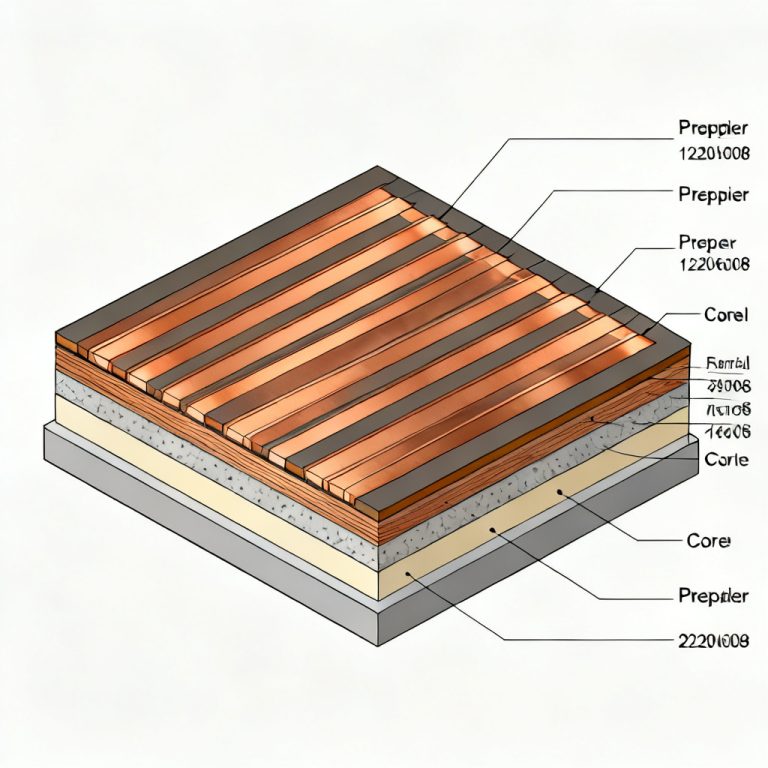
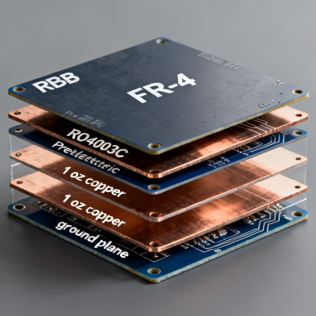
RF PCB layout guidelines for stack-up design require careful material selection and layer symmetry. The stack-up foundation defines impedance and return path quality.
1.1 Core vs. Prepreg Considerations
Core material provides stable dielectric constant (Dk) for critical RF layers. Prepreg Dk varies slightly during lamination. For tight impedance tolerances, use core materials for the primary RF signal layer. Always maintain symmetrical stack-up (e.g., 4-layer: Signal-Ground-Power-Signal) to prevent warpage during reflow.
1.2 Recommended Layer Counts for RF
2-layer boards suit simple, low-frequency RF below 1 GHz. 4-layer boards are gold standard for most RF designs up to 6 GHz: Layer 1 (Top) for RF components and microstrip traces; Layer 2 for solid ground plane; Layer 3 for power; Layer 4 for ground. 6+ layer boards are required for complex RF-plus-digital systems.
1.3 Dielectric Material Selection
FR-4 is acceptable only below 1-2 GHz due to uncontrolled Dk and high loss tangent. Rogers, Isola, or Taconic materials are mandatory above 2 GHz. Hybrid stack-ups use Rogers for top RF layers and FR-4 for lower digital layers to balance performance and cost.
2. RF PCB Layout Guidelines for Grounding
RF PCB layout guidelines emphasize that a continuous ground plane is the single most important rule. Poor grounding causes most RF failures.
2.1 The Continuous Ground Plane
Never route digital or power signals across the RF ground plane on Layer 2. This plane must be a solid, unbroken sheet of copper. Any slot or gap creates a large loop antenna, increasing inductance and causing radiation.
2.2 Grounding for Mixed-Signal Designs
Do not split the ground plane into analog and digital sections. Use a single, solid ground plane. Place RF components in one region and digital components in another. Use a keep-out zone on the component layer, but do not cut the underlying ground plane.
2.3 Via Fencing and Stitching
Place a row of vias along edges of RF traces, especially near PCB edges, to prevent unwanted waveguide modes. Connect ground pads of RF components directly to the ground plane with multiple vias. Use at least 3-4 vias per ground pad with spacing less than λ/20 at the highest operating frequency.
3. RF PCB Layout Guidelines for Transmission Lines
RF PCB layout guidelines require all RF traces to be designed as transmission lines with specific characteristic impedance, typically 50Ω.
3.1 Microstrip
Microstrip is a trace on top layer with ground plane directly below. It is easy to fabricate but more prone to radiation than stripline. Use a calculator with your stack-up Dk and height to find trace width.
3.2 Stripline
Stripline is a trace sandwiched between two ground planes. It offers excellent shielding but requires via transitions for component mounting. Trace width is typically narrower than microstrip for the same impedance.
3.3 Coplanar Waveguide (CPW)
CPW has a trace with ground planes on the same layer, separated by a gap. It provides good isolation and ground reference on the same layer. The gap should be at least the trace width.
3.4 Impedance Tolerances
Specify ±10% for standard designs and ±5% for critical matching networks. Your PCB manufacturer must provide impedance test coupons. We guarantee impedance control to ±5% on specified layers.
4. RF PCB Layout Guidelines for Component Placement
RF PCB layout guidelines state that placement is 80% of the layout battle. Think in terms of signal flow.
4.1 The Straight Line Rule
Arrange RF components in a straight line from input to output. Avoid U-turns or S-curves in the RF path. Example: Antenna Connector → BPF → LNA → Mixer → IF Filter in that exact linear order.
4.2 Decoupling Capacitors
Every active RF component needs decoupling. Place decoupling caps as close as possible to the power pin of the IC. The capacitor’s ground pad must connect to the ground plane with a dedicated via. Use a ferrite bead in series with the power supply line.
4.3 Keep-Out Zones
Never place ground vias or copper directly under the body of an inductor or critical RF component unless specified in the datasheet. Maintain 2x trace width clearance from other copper on the same layer.
5. RF PCB Layout Guidelines for Trace Routing
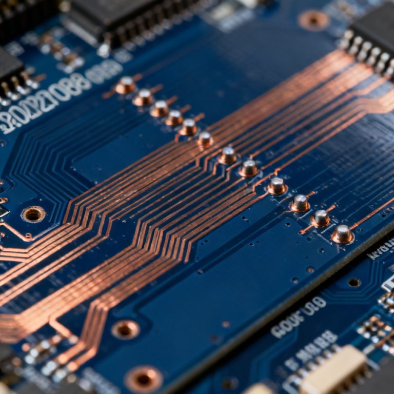
RF PCB layout guidelines for routing require 45-degree corners, consistent trace width, and minimized via transitions.
5.1 The 45-Degree Rule
A 90-degree corner creates impedance discontinuity and signal reflection. Use 45-degree chamfered corners or smooth arcs for all RF traces. Mitered bends are best for critical high-power paths.
5.2 Trace Width Consistency
Do not change trace width unless designing an impedance transformer. If you must change width, use a smooth taper of at least 3x the wavelength.
5.3 Via Transitions
A standard via has inductance of ~1 nH. Minimize vias for RF signals. If you must change layers, use back-drilled vias to remove unused stubs. Place a ground via immediately adjacent to the signal via when changing layers.
5.4 Isolation Between Traces
Keep RF traces as far apart as possible. Use 3W spacing for moderate isolation and 5W for high isolation. Place grounded guard traces between critical paths.
6. RF PCB Layout Guidelines for Thermal Management
RF PCB layout guidelines for high-power amplifiers require thermal vias and thicker copper.
6.1 Thermal Vias
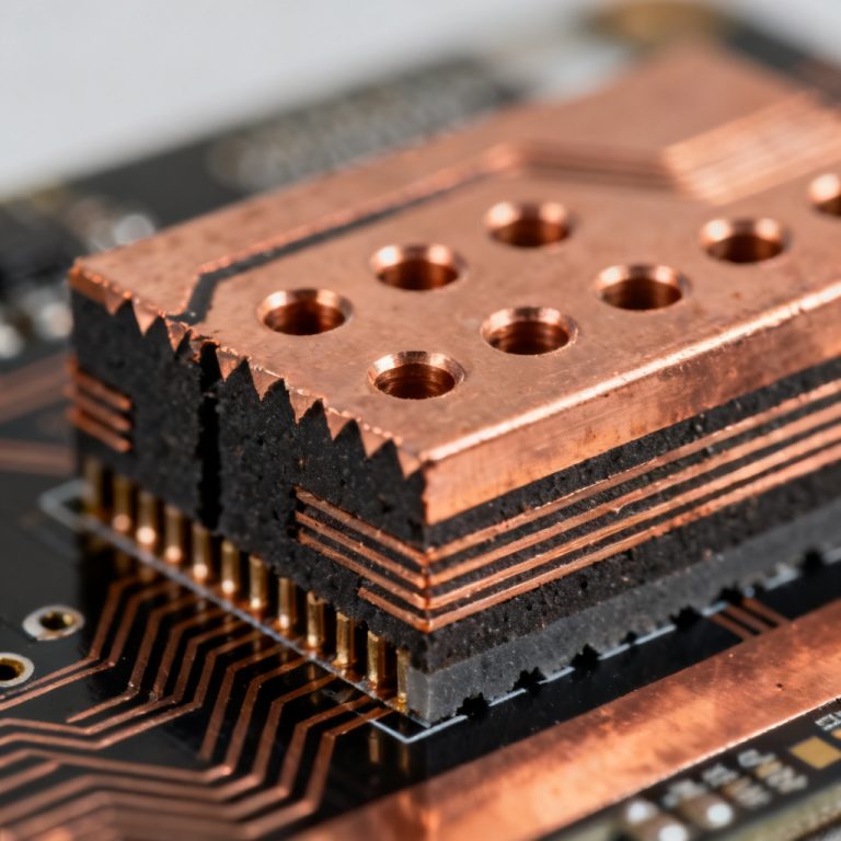
Place a dense array of thermal vias directly under the exposed pad of the PA. Connect these vias to a solid copper pour on the bottom layer as a heat spreader.
6.2 Copper Thickness
Use 2 oz or 3 oz copper for outer layers of high-power RF sections to reduce resistive losses and conduct heat away from the die.
7. RF PCB Layout Guidelines for Shielding
RF PCB layout guidelines for EMI control include using RF shields and maintaining PCB edge clearance.
7.1 RF Shields
Use metal shields over sensitive or noisy sections. The shield must make excellent contact with the ground plane using a continuous perimeter of vias with spacing less than λ/20.
7.2 PCB Edge Clearance
Do not route traces or copper within 50-100 mils of the PCB edge. Place a ground ring around the entire board perimeter, stitched to internal ground planes every 100-200 mils.
8. RF PCB Layout Guidelines for Power Supply Decoupling
RF PCB layout guidelines for power decoupling require bulk, mid-frequency, and high-frequency capacitors. Place a 10 µF capacitor near the DC power entry point. Place 0.1 µF capacitors close to each active device. Place 100 pF capacitors as close to the power pin as possible. Use the power island technique for sensitive circuits.
9. RF PCB Layout Guidelines: Final Checklist
Before sending your design to fabrication, verify these points: stack-up with RF signal layer adjacent to solid ground plane; impedance trace widths calculated for exact stack-up; ground pads stitched with multiple vias; decoupling caps placed as close as possible; TX and RX paths separated by at least 3W; RF vias back-drilled; all traces using 45-degree bends; ground ring around PCB perimeter. See PCB Principles to know how is this checklist base on: PCB principles and fundamentals.
10. Frequently Asked Questions
What are the most critical RF PCB layout guidelines?
The most critical RF PCB layout guidelines include continuous grounding, controlled impedance, and proper component placement to ensure signal integrity and minimize EMI.
How do I choose the right stack-up for RF PCB design?
Follow RF PCB layout guidelines by selecting materials with stable Dk, using symmetrical stack-ups, and placing RF signal layers immediately adjacent to solid ground planes.
Why is via stitching important in RF PCB layout?
Via stitching reduces ground inductance and prevents unwanted waveguide modes, as emphasized in RF PCB layout guidelines for maintaining low-impedance return paths.
What is the recommended trace width for 50Ω impedance?
According to RF PCB layout guidelines, trace width depends on stack-up height and Dk. Use a transmission line calculator with your specific stack-up parameters.
How do I ensure proper isolation between RF traces?
RF PCB layout guidelines recommend 3W to 5W spacing between traces and using grounded guard traces for critical isolation between TX and RX paths.
What materials are best for high-frequency RF PCBs?
RF PCB layout guidelines specify Rogers, Isola, or Taconic materials for frequencies above 2 GHz due to stable Dk and low loss tangent.
RF PCB Layout Guidelines: Comparison Table
| RF PCB Layout Guidelines Parameter | Standard Design | Critical Design |
|---|---|---|
| Impedance Tolerance | ±10% | ±5% |
| Via Spacing | λ/10 | λ/20 |
| Trace Clearance | 2W | 5W |
| Dielectric Material | FR-4 | Rogers/Isola |
| Copper Thickness | 1 oz | 2-3 oz |
RF PCB Layout Guidelines: Industry Terminology
Impedance control ensures consistent characteristic impedance along transmission lines. Microstrip is a trace on top layer with ground plane below. Stripline is a trace between two ground planes. Via stitching connects ground pads to the ground plane with multiple vias. Back-drilling removes unused via stubs to prevent resonance. Dielectric constant (Dk) affects signal velocity and impedance. Loss tangent measures signal attenuation in the substrate.