Signal Integrity Impedance Control Guide for High‑Speed PCBs
Signal Integrity Impedance Control Guide for High Speed PCBs. This guide covers trace geometry, stackup planning, material selection, and simulation techniques to ensure reliable performance above 1 Gbps.
Core Concepts of Signal Integrity & Impedance Control
Characteristic Impedance (Z₀) for High‑Speed PCBs
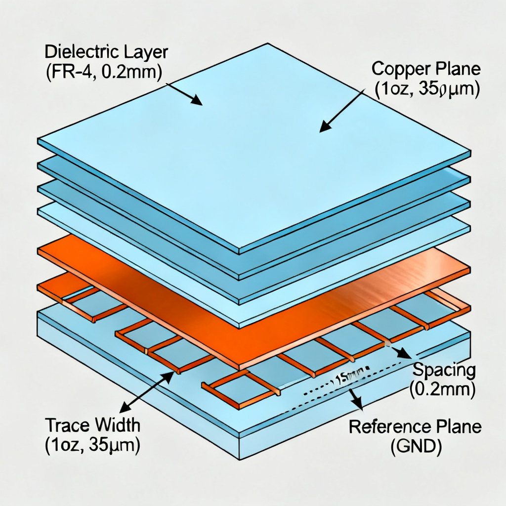
Characteristic impedance is the resistance a transmission line presents to a propagating signal. For high‑speed PCB signal integrity, it depends on trace width (W), trace thickness (T), dielectric height (H), and dielectric constant (Dk).
Transmission Line Types in Impedance Control
Microstrip and stripline are the primary transmission lines in high‑speed PCB impedance control. Microstrip is on outer layers; stripline is embedded between reference planes. Differential pairs target 100Ω for standards like USB and HDMI.
Impedance Calculation Formulas
From IPC‑2141: Microstrip Z₀ = 87/√(εr+1.41) * ln(5.98H/(0.8W+T)). Stripline Z₀ = 60/√εr * ln(4H/(0.67π(0.8W+T))). Always use a field solver like Polar SI9000 for production.
PCB Stackup Design for Signal Integrity & Impedance Control
Stackup Planning Fundamentals
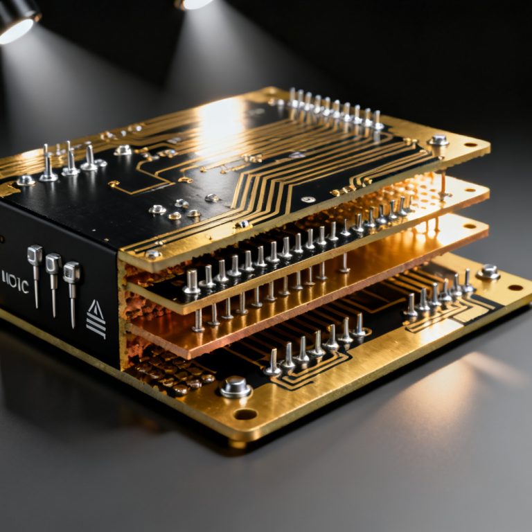
A well‑designed stackup is the foundation of high‑speed PCB signal integrity. Common stackups include 4‑layer (Signal‑GND‑Power‑Signal) and 6‑layer (Signal‑GND‑Signal‑Power‑GND‑Signal).
Key Stackup Rules for Impedance Control
Every signal layer must have an adjacent solid reference plane. Symmetry prevents warpage. Dielectric thickness determines trace width for target impedance. Specify 50Ω ±10% single‑ended and 100Ω ±10% differential.
Material Selection for High‑Speed PCBs
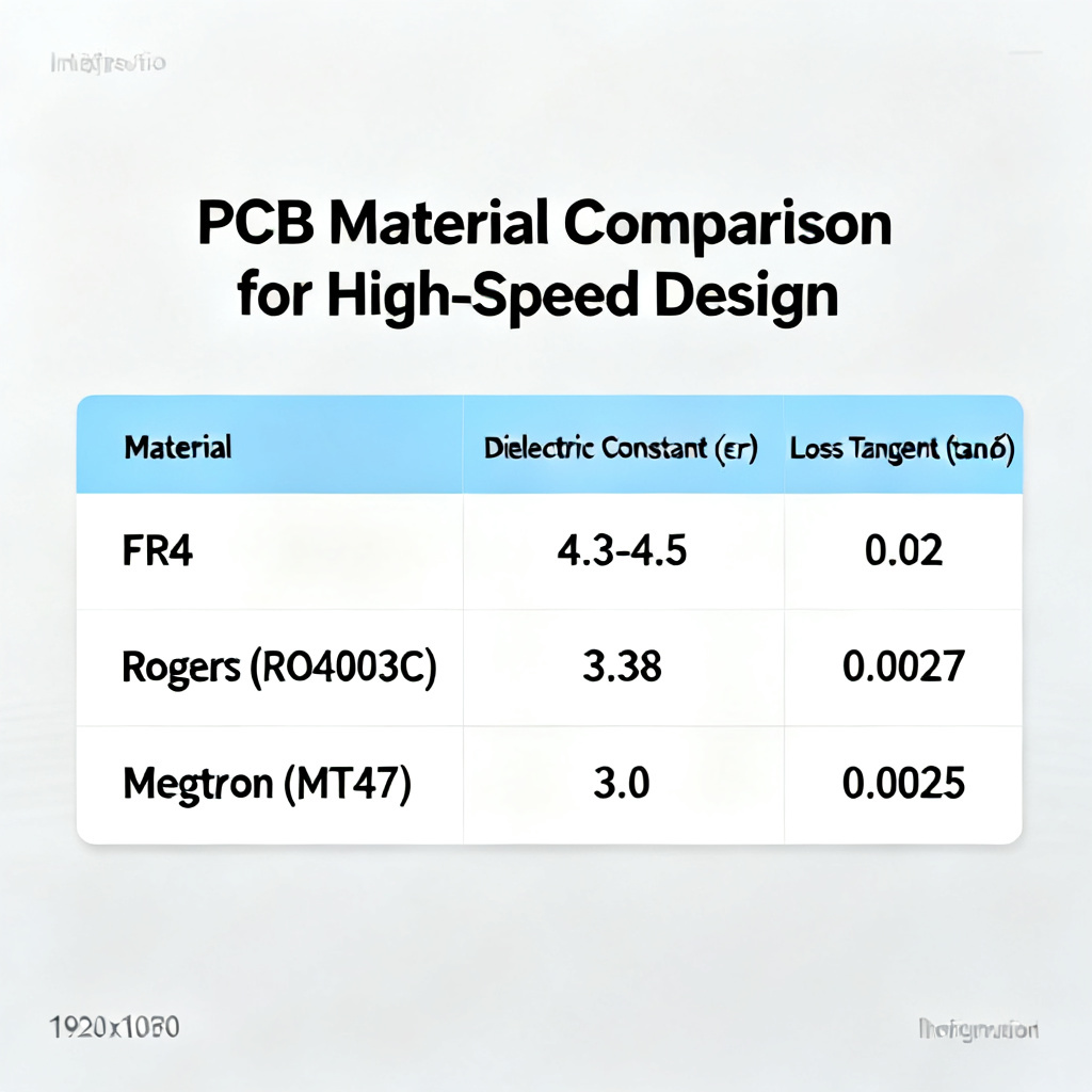
FR‑4 is suitable up to 3 Gbps. High‑speed FR‑4 (e.g., Isola 370HR) works for 3–10 Gbps. Low‑loss materials (Rogers 4350B, Megtron 6) are ideal above 10 Gbps. PTFE offers lowest loss but is expensive.
Trace Geometry and Routing Best Practices
Trace Width and Spacing in High‑Speed PCB Design
For 50Ω microstrip on 0.2mm prepreg, width is ~0.3mm. Differential pairs require identical width and spacing. Maintain 3H spacing to minimize crosstalk; use 5H for critical signals.
Routing Guidelines for Signal Integrity
Avoid 90° corners; use 45° chamfers. Keep traces short to reduce loss. Minimize vias; each adds capacitance and inductance. Use back‑drilling for high‑speed signals. Match differential pair lengths within 5 mils.
Impedance Discontinuities in High‑Speed PCBs
Common sources include via transitions, connector pads, and layer changes. Add stitching vias near signal vias. Use teardrops for smooth transitions. Provide return vias for layer changes.
Simulation and Verification for Impedance Control
Pre‑Layout Simulation
Use 2D field solvers like Polar SI9000 for impedance calculation. 3D solvers like Ansys HFSS handle complex structures. IBIS models simulate eye diagrams and jitter.
Post‑Layout Verification
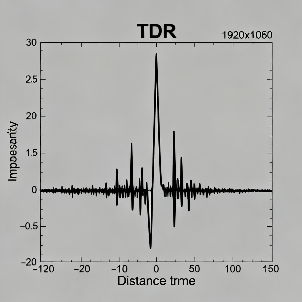
TDR measures impedance profile along a trace. VNA measures S‑parameters up to 40 GHz. Eye diagram testing quantifies signal quality. Design with margin for manufacturing tolerances.
Advanced Topics in Signal Integrity & Impedance Control
Crosstalk and Coupling
NEXT and FEXT occur due to electromagnetic coupling. Mitigate by increasing spacing, using guard traces, and routing critical signals on different layers.
Skin Effect and Dielectric Loss
At high frequencies, skin effect increases resistance. Dielectric loss (tan δ) attenuates signals. Use low‑loss materials and wider traces to reduce loss.
Return Path and Grounding
Every signal needs a continuous return path. Use ground planes instead of traces. Stitch ground planes with vias at every 1/20 wavelength of the highest frequency.
Practical Design Checklist for Engineers
1. Define targets: Z₀, tolerance, data rate, material. 2. Design stackup with solid reference planes. 3. Select materials matching Dk and Df. 4. Calculate trace geometry using field solver. 5. Route carefully: avoid 90°, maintain spacing, match lengths. 6. Simulate pre‑layout and post‑layout. 7. Specify manufacturing with impedance coupons. 8. Verify with TDR or VNA on prototypes.
Conclusion
Signal integrity and impedance control are not optional in high‑speed PCB design. By understanding transmission line theory, designing a proper stackup, selecting the right materials, and following rigorous routing and simulation practices, you can achieve reliable, high‑performance boards. Partner with a PCB manufacturer that offers impedance testing and tight tolerance control.
Frequently Asked Questions
What is signal integrity in high‑speed PCBs?
Signal integrity refers to the quality of an electrical signal as it travels through a PCB. For high‑speed PCBs, impedance control is essential to prevent reflections and maintain signal quality.
How do I calculate impedance for my PCB?
Use a field solver like Polar SI9000 with your stackup parameters. Target 50Ω single‑ended or 100Ω differential for most high‑speed applications.
What materials are best for high‑speed signal integrity?
Low‑loss materials like Rogers 4350B or Megtron 6 are ideal above 10 Gbps. High‑speed FR‑4 works for 3–10 Gbps. Always match Dk and Df to your frequency needs.
Why is impedance control important for high‑speed PCBs?
Impedance control minimizes reflections, reduces EMI, and ensures clean signal transitions. Without it, data errors and system failures occur.
How can I verify impedance in my PCB design?
Use TDR or VNA on prototype boards. Include impedance coupons on the panel for manufacturing verification.
Comparison: Our Impedance Control Services vs. Industry Standards
| Parameter | Industry Standard | Our High‑Speed PCB Service |
|---|---|---|
| Impedance Tolerance | ±10% | ±5% |
| Material Options | FR‑4 only | FR‑4, High‑Speed FR‑4, Rogers, Megtron |
| Testing | Coupon only | Coupon + TDR/VNA on request |
| Stackup Support | Standard 4‑layer | 4 to 20+ layers, custom stackups |
Glossary of Key Terms
Characteristic Impedance (Z₀): The impedance a transmission line presents to a propagating signal, critical for high‑speed PCB signal integrity.
Dielectric Constant (Dk): A material property affecting impedance; higher Dk lowers impedance.
Differential Pair: Two traces carrying equal and opposite signals, commonly used for 100Ω impedance control in high‑speed PCBs.
Stripline: A transmission line embedded between two reference planes, offering better isolation than microstrip.
TDR: Time Domain Reflectometry, a method to measure impedance profile along a trace.