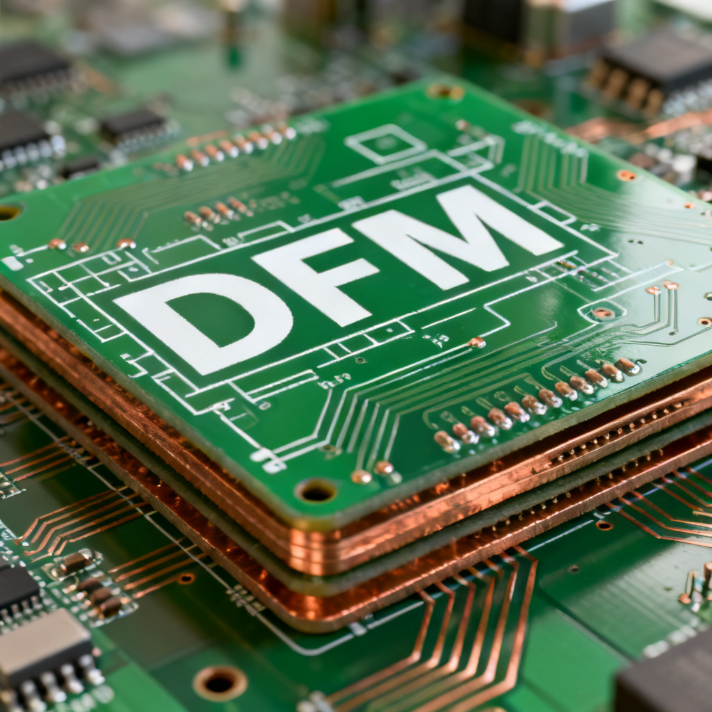
PCB DFM Guidelines Rules to Improve Yield Lower Rework
PCB DFM Guidelines Rules to Improve Yield Lower Rework are essential for manufacturers aiming to reduce defects and optimize production efficiency. By integrating these design for manufacturability principles early in the PCB design process, you significantly improve yield and lower rework costs, ensuring consistent quality for custom PCB orders.
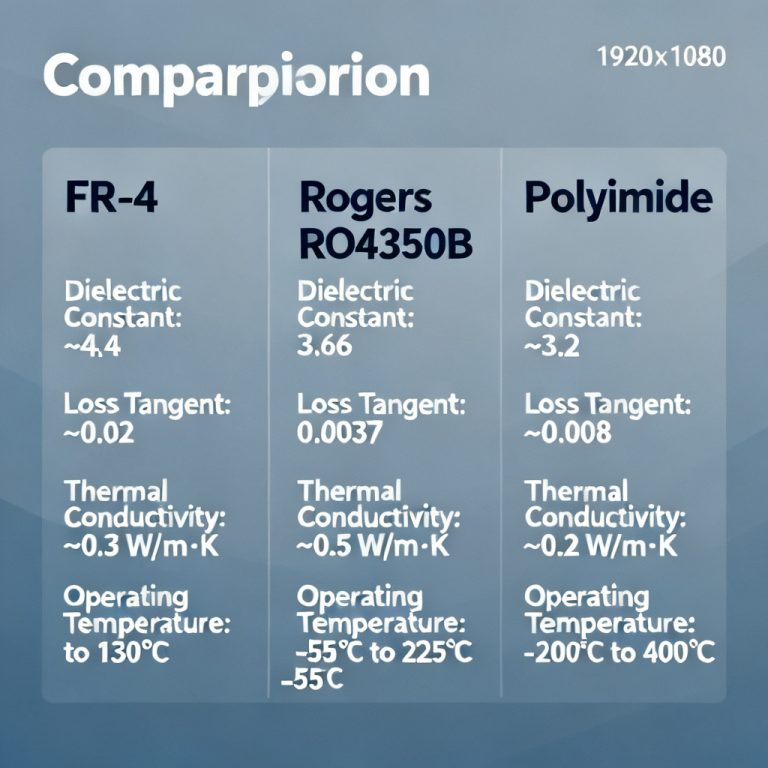
PCB DFM Guidelines: Material Selection & Stackup
Standard Materials for High Volume
For high yield, choose standard FR-4 materials like IT-180 or 370HR. These PCB DFM guidelines emphasize avoiding exotic substrates unless electrical requirements demand them. Standard materials are pre-qualified, reducing lead times and defects.
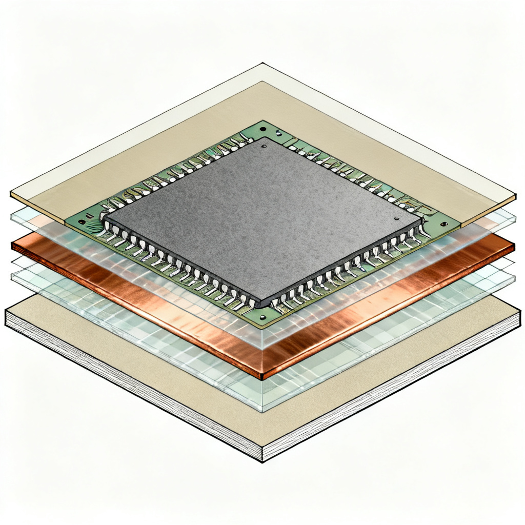
Optimize Copper Weight
Use 1 oz copper as default for most signal layers. For power circuits, 2 oz is acceptable but requires wider traces. These design for manufacturability rules ensure consistent etching and prevent opens.
Controlled Impedance Stackup
Provide a symmetrical stackup to prevent warpage. Specify dielectric constant (Dk) and dissipation factor (Df) for impedance control. This aligns with PCB DFM guidelines for high-speed designs.
| Parameter | Standard Rule | Tolerance |
|---|---|---|
| Copper weight | 1 oz (35µm) | ±10% |
| Min trace/space (1 oz) | 5 mil (0.127mm) | ±0.5 mil |
| Min hole size | 0.2mm (8 mil) | ±0.05mm |
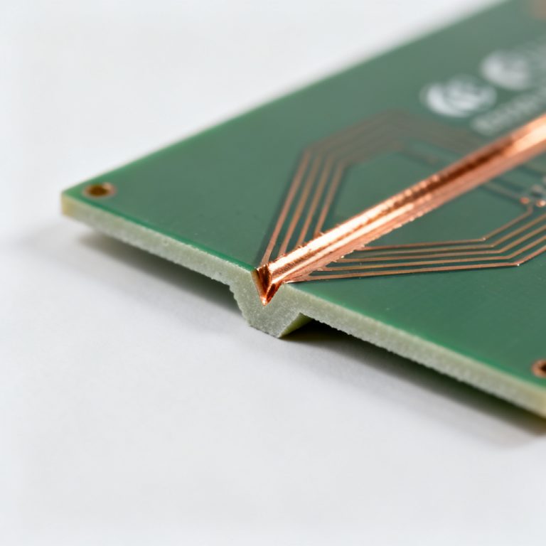
PCB DFM Guidelines: Trace, Space & Copper Balance
Minimum Trace Width and Spacing
Maintain 6 mil trace/space for standard production to maximize yield. These PCB DFM guidelines reduce etching variations and solder bridging risks.
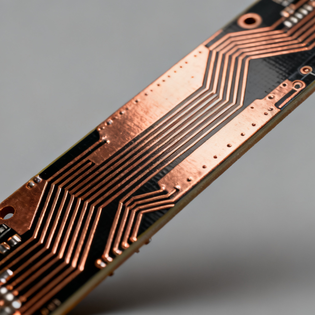
Copper Balancing
Use copper thieving to achieve >70% copper density per layer. This prevents differential etching and improves improve yield outcomes.
Avoid Acute Angles
Use 45° chamfered corners to prevent etchant trapping. This is a critical design for manufacturability rule for reliable etching.
PCB DFM Guidelines: Vias, Holes & Pads
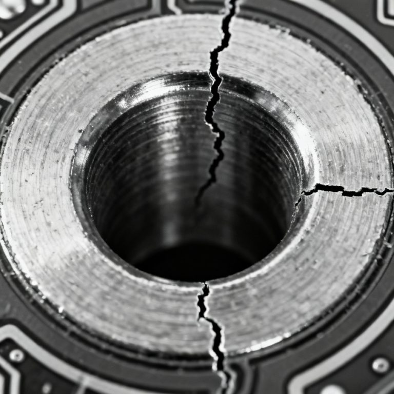
Minimum Hole Size & Aspect Ratio
Keep aspect ratio ≤10:1 for reliable plating. For 1.6mm boards, hole diameter must be ≥0.16mm. These PCB DFM guidelines prevent barrel cracks.
Via-in-Pad Caution
Fill vias in pads with epoxy to avoid solder wicking. This lower rework strategy ensures proper fillet formation.
Annular Ring Requirements
Design annular rings of at least 0.075mm for external layers. Insufficient rings cause breakout and open circuits.
| Parameter | Standard Rule | Tolerance |
|---|---|---|
| Min annular ring (external) | 0.075mm (3 mil) | ≥2 mil |
| Min hole size | 0.2mm (8 mil) | ±0.05mm |
| Aspect ratio | ≤10:1 | ≤12:1 for HDI |
PCB DFM Guidelines: Solder Mask & Silkscreen
Solder Mask Clearance & Web
Maintain 0.1mm solder mask web to prevent slivers. These PCB DFM guidelines ensure mask adhesion and prevent shorts.
Silkscreen Placement
Never place silkscreen on pads or bare copper. Keep text at least 0.15mm from pad edges for reliable soldering.
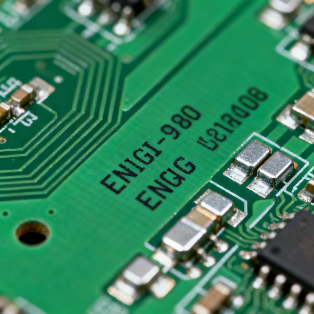
Surface Finish Selection
Use ENIG for fine-pitch components and HASL for high-volume designs. This design for manufacturability choice improves solderability.
PCB DFM Guidelines: Panelization & Fiducials
Panelization Rules
Use tooling holes and V-grooves for consistent assembly. Proper panelization reduces handling defects and improves improve yield.
Fiducial Marks
Place three global fiducials per panel for accurate SMT placement. This is a key PCB DFM guideline for automated assembly.
Test Point Clearance
Design test points on a 0.1-inch grid with 1mm pads for reliable probing.
PCB DFM Guidelines: Thermal Management
Thermal Relief for Through-Hole Pads
Use 4-spoke thermal reliefs to facilitate soldering. Solid connections cause cold joints and increase lower rework needs.
Copper Pour Clearance
Maintain 0.2mm clearance between pours and pads to prevent arcing and parasitic capacitance.
PCB DFM Guidelines: Final Verification Checklist
| Parameter | Standard Rule | Acceptable Tolerance |
|---|---|---|
| Min trace/space | 5 mil (0.127mm) | ±0.5 mil |
| Min hole size | 0.2mm (8 mil) | ±0.05mm |
| Annular ring (external) | 0.075mm (3 mil) | ≥2 mil |
| Solder mask web | 0.1mm (4 mil) | ≥3 mil |
| Copper balance | >70% per layer | ±10% |
| Aspect ratio | ≤10:1 | ≤12:1 for HDI |
| Fiducial size | 1mm pad, 3mm clearance | ±0.1mm |
By adhering to these PCB DFM guidelines, you transform your design into a manufacturable product. Each rule is designed to improve yield and lower rework, ensuring cost-effective production. For custom PCB orders, our engineering team provides a free DFM review to guarantee first-pass success.
Comparison: Standard vs. Optimized DFM Approach
Standard designs often ignore copper balance and thermal relief, leading to higher defect rates. Our PCB DFM guidelines prioritize symmetry and clearance, reducing rework by up to 30%. This professional approach ensures consistent quality without compromising performance.
Industry Terminology Explained
Aspect ratio: Ratio of board thickness to hole diameter, critical for plating reliability. Annular ring: Copper pad width around a drilled hole. Copper thieving: Dummy copper patterns to balance density. Solder mask web: Gap between mask openings preventing slivers. Thermal relief: Spoked connection for heat dissipation during soldering.
FAQ: PCB DFM Guidelines
What are PCB DFM guidelines?
PCB DFM guidelines are design rules that improve yield and lower rework by optimizing layouts for manufacturing processes.
How do DFM rules lower rework costs?
By preventing common defects like etching errors and solder bridging, design for manufacturability reduces the need for costly rework cycles.
What is the most important DFM rule for high yield?
Maintaining copper balance and proper trace/space ratios is critical to improve yield in high-volume production.