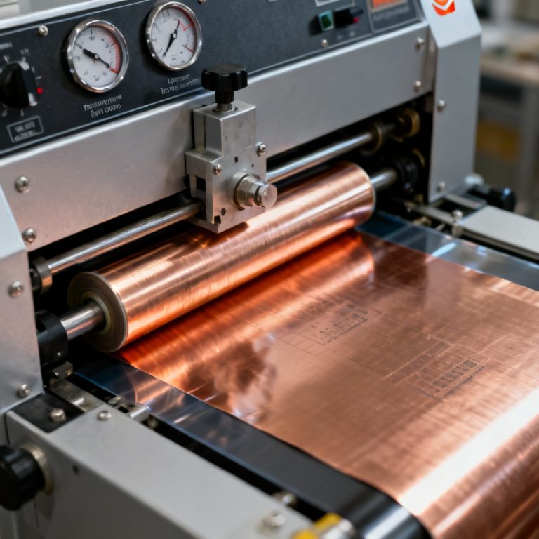
Inner Layer Imaging and Etching for Multilayer PCBs
In the world of advanced electronics, inner layer imaging and etching for multilayer PCBs define the quality, reliability, and functionality of high-density devices. Unlike simple double-sided boards, multilayer PCBs consist of several layers of conductive copper and insulating dielectric material, laminated together under heat and pressure. The quality, reliability, and functionality of these boards hinge…