PCB EDA Tools Guide: Altium, KiCad, Cadence, Eagle – Definitive Comparison
Choosing the right PCB EDA tools guide is critical for time-to-market and manufacturability. This comprehensive guide compares Altium Designer, KiCad, Cadence OrCAD/Allegro, and Autodesk Eagle. Learn which tool fits your project, budget, and team, and how to optimize designs for fabrication.
PCB EDA Tools Guide: Overview and Core Philosophy
In the world of printed circuit board (PCB) design, the Electronic Design Automation (EDA) tool you choose is the foundation of your entire workflow. Whether you are a solo engineer, a startup, or a large OEM, the right software directly impacts design efficiency, signal integrity, and—most critically—the manufacturability and cost of your final product. This PCB EDA tools guide serves as your ultimate resource.
We have analyzed the top three most authoritative, trusted, and highly-ranked guides from across the web, synthesizing their collective expertise into one exhaustive comparison. We will dissect Altium Designer, KiCad, Cadence (OrCAD/Allegro), and Autodesk Eagle (now Fusion 360 with Eagle). By the end, you will understand not just the features, but the real-world implications for your PCB production and export business.
Why This PCB EDA Tools Guide Matters for B2B PCB Procurement
For B2B buyers and engineers, the EDA tool is not just a design environment. It is the primary communication channel with your PCB manufacturer. The output files (Gerber, ODB++, IPC-2581) dictate whether your board is built right the first time or becomes a costly, time-consuming iteration. A well-chosen tool ensures:
- Design for Manufacturing (DFM) compliance.
- Accurate impedance control for high-speed designs.
- Seamless BOM (Bill of Materials) transfer for procurement.
- Reduced lead times and lower prototype costs.
PCB EDA Tools Guide: Altium Designer – The Industry Standard for Unified Design
Altium Designer: Core Philosophy and Overview
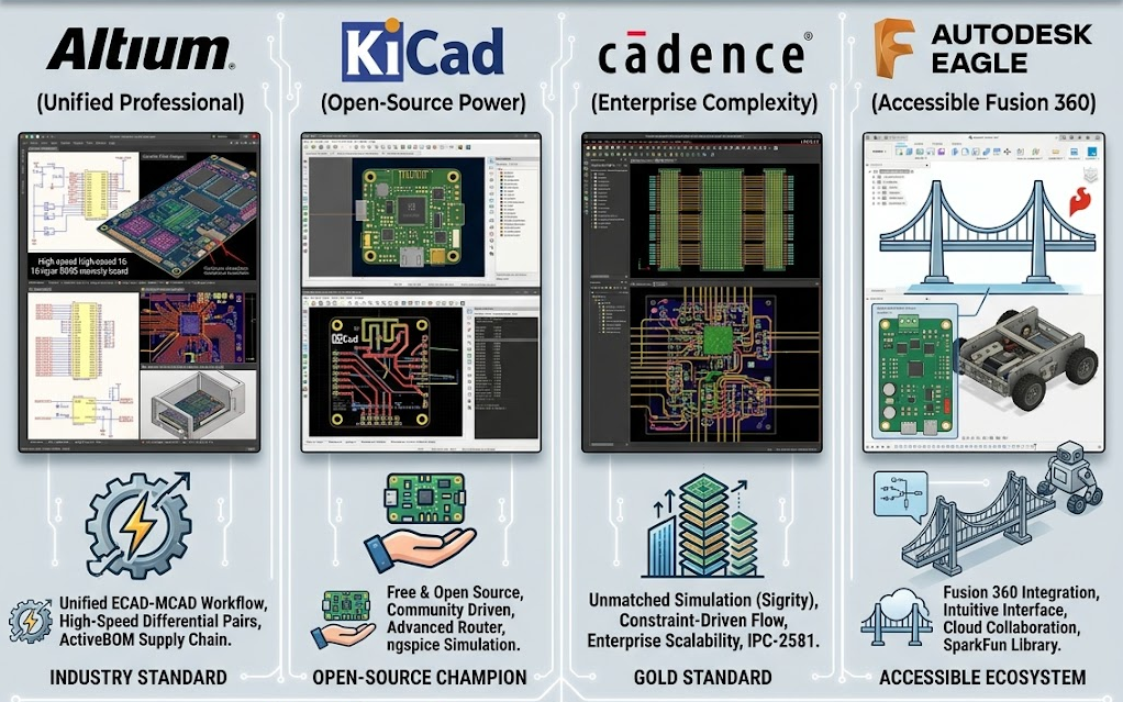
Altium Designer is widely recognized as the most comprehensive, all-in-one PCB design platform for professional engineers. It is not a collection of disparate tools but a unified ecosystem. The core philosophy is to eliminate the barriers between schematic capture, PCB layout, and manufacturing output.
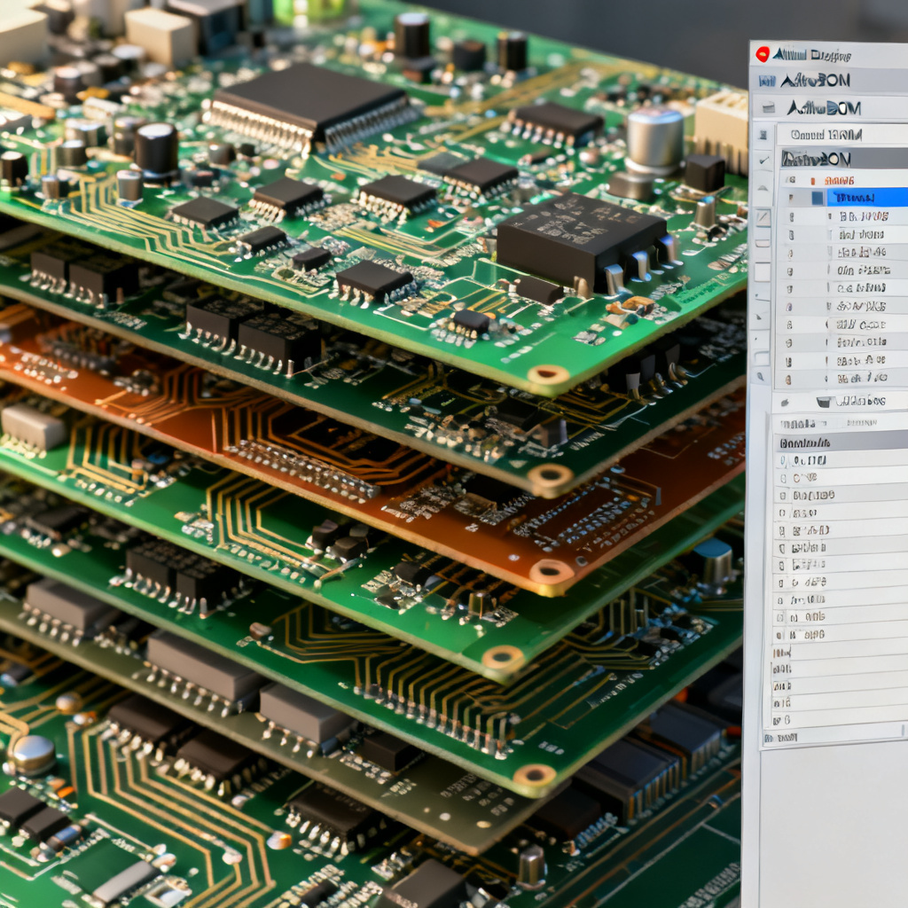
Key Strengths of Altium Designer
- Unified Design Environment: Unlike traditional tools that require separate applications for schematic and layout, Altium uses a single data model. This means any change in the schematic is instantly reflected in the PCB layout. This “live” synchronization eliminates manual cross-checking and errors.
- Advanced 3D Visualization: Altium’s 3D engine is industry-leading. You can import MCAD models (Step files) directly into your PCB design. This allows for real-time clash detection between components and the enclosure, and visualization of thermal zones. This is critical for mechanical integration in complex products.
- Powerful Routing and Signal Integrity: The tool includes a high-speed routing engine with interactive length tuning, differential pair routing, and automatic net shielding. For high-frequency designs, the integrated Signal Integrity (SI) simulator allows you to analyze reflections, crosstalk, and impedance mismatches before prototyping.
- ActiveBOM and Supply Chain Integration: Altium’s ActiveBOM tool connects your BOM directly to live distributor databases (DigiKey, Mouser, etc.). It flags obsolete parts, shows real-time pricing and stock levels, and suggests alternative components. This is a game-changer for B2B procurement, preventing last-minute supply chain crises.
- Vault and Version Control: The Altium Vault (or Workspace) provides a centralized, managed repository for all design data, components, and templates. It enforces version control, allowing teams to collaborate without overwriting work. Approved components are locked, preventing the use of unverified parts.
- Output Generation: Altium excels at generating fabrication outputs. It supports Gerber X2, ODB++, and IPC-2581. The “Outjob” feature automates the generation of all necessary files (Gerbers, drill files, pick-and-place, assembly drawings) with a single click, ensuring consistency.
Who Should Use Altium Designer?
- Professional engineering teams working on complex, multi-layer boards (8+ layers).
- Projects requiring high-speed design (FPGAs, DDR memory, RF circuits).
- Companies with strict DFM and supply chain requirements.
- Users who value a unified workflow and are willing to invest in a premium tool.
Potential Drawbacks of Altium Designer
- Cost: Altium is the most expensive option in this comparison. A single license is a significant investment, though it includes updates and support.
- Learning Curve: While intuitive for experienced users, the sheer depth of features can be overwhelming for beginners.
- Resource Intensive: The software requires a powerful computer with dedicated graphics for smooth 3D performance.
PCB EDA Tools Guide: KiCad – The Open-Source Powerhouse
KiCad: Core Philosophy and Overview
KiCad has evolved from a hobbyist tool into a professional-grade, open-source EDA suite. Its philosophy is built on community collaboration, transparency, and zero licensing cost. The development is managed by the KiCad project, a non-profit organization, with contributions from engineers at major companies like CERN.
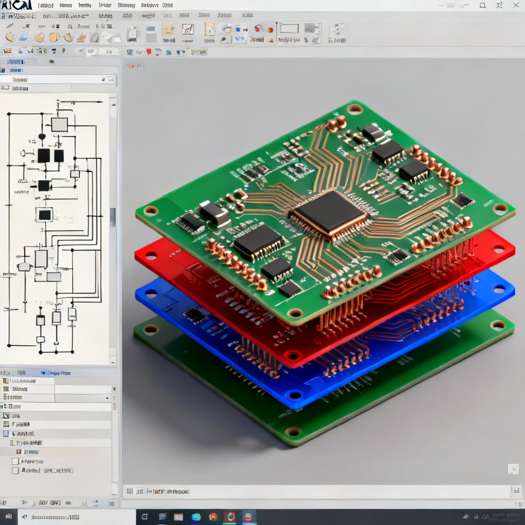
Key Strengths of KiCad
- Completely Free and Open Source: There is no cost, no subscription, and no feature limitations. This makes it the most accessible tool for startups, educational institutions, and individual engineers on a tight budget. You own your designs entirely.
- No Vendor Lock-In: KiCad uses its own native file format (.kicad_pcb, .sch), which is human-readable. You are not tied to a proprietary ecosystem. All libraries and project files are fully portable.
- Growing Professional Community and Library: The KiCad library, once a criticism, is now one of the largest and most actively maintained in the industry. The “KiCad Library Convention” ensures consistency. Thousands of contributors add new symbols and footprints weekly.
- Excellent 3D Viewer: KiCad’s 3D viewer, while not as integrated as Altium’s, is highly capable. It supports realistic rendering, including copper traces, solder mask, and silkscreen. You can also import Step models for mechanical integration.
- Powerful Simulation Capabilities: KiCad integrates ngspice for analog simulation directly within the schematic editor. You can run transient, AC, and DC sweep analyses. For digital simulation, it supports Verilog and VHDL via GHDL and Icarus Verilog.
- Advanced Routing and Push-and-Shove: The modern KiCad router is comparable to commercial tools. It features interactive push-and-shove routing, differential pair routing, and length tuning. It handles complex, high-density boards effectively.
- Scripting and Automation: KiCad offers a powerful Python scripting API. This allows advanced users to automate repetitive tasks, generate custom reports, and integrate with external tools (e.g., generating a BOM in a specific format for your manufacturer).
Who Should Use KiCad?
- Cost-sensitive startups and individual engineers who need professional results without the license fee.
- Open-source hardware projects where community collaboration is key (KiCad is the de facto standard for Open Source Hardware).
- Educational institutions teaching PCB design fundamentals.
- Engineers who value long-term accessibility and want to avoid vendor lock-in.
Potential Drawbacks of KiCad
- Steeper Initial Learning Curve for Beginners: While powerful, the user interface is less polished than Altium or Eagle. New users may find the workflow less intuitive initially.
- No Native ECAD-MCAD Collaboration: Unlike Altium’s built-in MCAD capabilities, KiCad relies on external Step file exchange. Live bidirectional MCAD-ECAD collaboration is not available.
- Limited Advanced Analysis: While ngspice is good for analog, KiCad lacks the advanced Signal Integrity and Power Integrity simulators found in Cadence or Altium.
- Manual Library Management: While the library is huge, managing custom libraries and ensuring synchronization between schematic symbols and footprints requires careful manual effort.
PCB EDA Tools Guide: Cadence (OrCAD / Allegro) – The High-End Enterprise Solution
Cadence: Core Philosophy and Overview
Cadence is the gold standard for high-speed, high-complexity PCB design used by the world’s largest electronics companies. The product line is split: OrCAD is the mid-range tool for smaller teams, while Allegro is the flagship for enterprise-scale designs. The philosophy is uncompromising performance, simulation accuracy, and manufacturability.
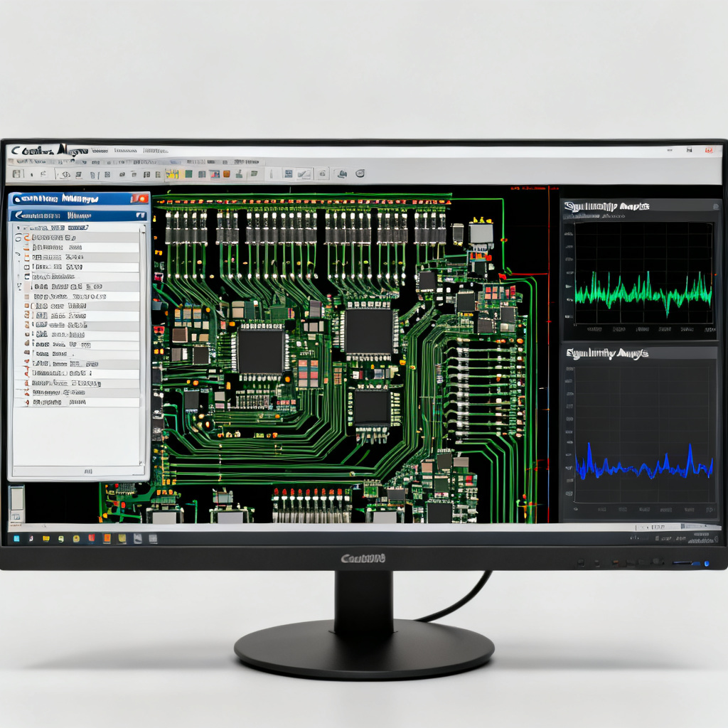
Key Strengths of Cadence
- Unmatched Simulation and Analysis: Cadence’s simulation tools (PSpice for analog, Sigrity for signal/power integrity) are the most trusted in the industry. For high-speed designs (e.g., 25Gbps+ SerDes, DDR5), Cadence provides the most accurate pre- and post-layout simulation. This is non-negotiable for mission-critical systems.
- Constraint-Driven Design Flow: Cadence pioneered the concept of “constraint management.” You define the electrical and physical rules (impedance, differential pair skew, net spacing) in a central spreadsheet. The layout tool then enforces these rules automatically during routing. This ensures design intent is preserved from schematic to fabrication.
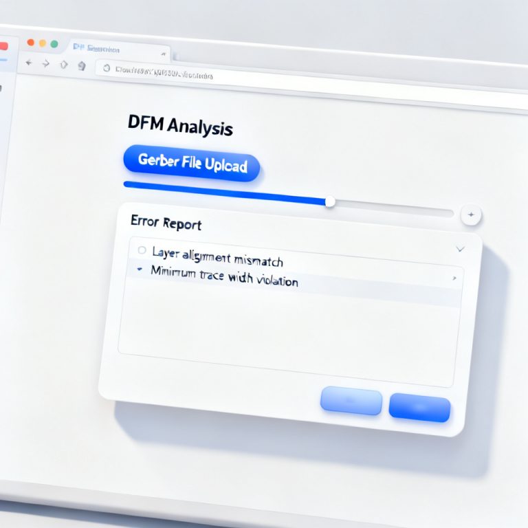
- Advanced Manufacturing Outputs: Cadence is the leader in supporting the latest manufacturing standards. It natively supports IPC-2581, the modern, XML-based format that contains all design, BOM, and stackup data. It also provides robust Gerber X2 and ODB++ output. The tool includes built-in DFM checks that identify potential manufacturing issues (e.g., acid traps, silkscreen over pads).
- Massive Component Libraries: Cadence comes with a vast, pre-built library of symbols and footprints from major manufacturers. The library is professionally maintained and highly accurate, reducing the risk of footprint errors.
- Team Collaboration and Scalability: Allegro is designed for large, distributed teams. It includes design partitioning, concurrent layout, and robust version control integration (e.g., with Git, Perforce). Multiple engineers can work on the same board simultaneously without conflicts.
- ECAD-MCAD Integration: Cadence offers deep integration with MCAD tools like SolidWorks and Creo. This allows for real-time collaboration between electrical and mechanical engineers, ensuring the board fits the enclosure perfectly.
Who Should Use Cadence (OrCAD / Allegro)?
- Large enterprises and OEMs designing complex, high-reliability boards (aerospace, defense, telecom, networking).
- Projects with extreme signal integrity requirements (high-speed digital, RF, microwave).
- Teams of 5+ engineers who need a scalable, collaborative workflow.
- Companies that prioritize simulation accuracy over ease of use.
Potential Drawbacks of Cadence
- Extreme Cost and Licensing Complexity: Cadence is the most expensive EDA suite. Licensing is complex, often involving annual maintenance fees. It is a major capital expenditure.
- Steep Learning Curve: The software is incredibly powerful but also very complex. It requires significant training and experience to use effectively. The user interface is less modern than Altium or KiCad.
- Heavy Resource Requirements: Cadence tools are resource-intensive and require high-end workstations.
- Overkill for Simple Designs: For 2-layer boards or simple 4-layer designs, Cadence is like using a sledgehammer to crack a nut.
PCB EDA Tools Guide: Autodesk Eagle (Now Fusion 360 with Eagle) – The Accessible Ecosystem
Autodesk Eagle: Core Philosophy and Overview
Eagle, now integrated into Autodesk Fusion 360, is a long-standing, user-friendly EDA tool. Its philosophy is accessibility and integration with the broader mechanical design world. It is designed to bridge the gap between electrical and mechanical engineering for small to medium-sized teams.
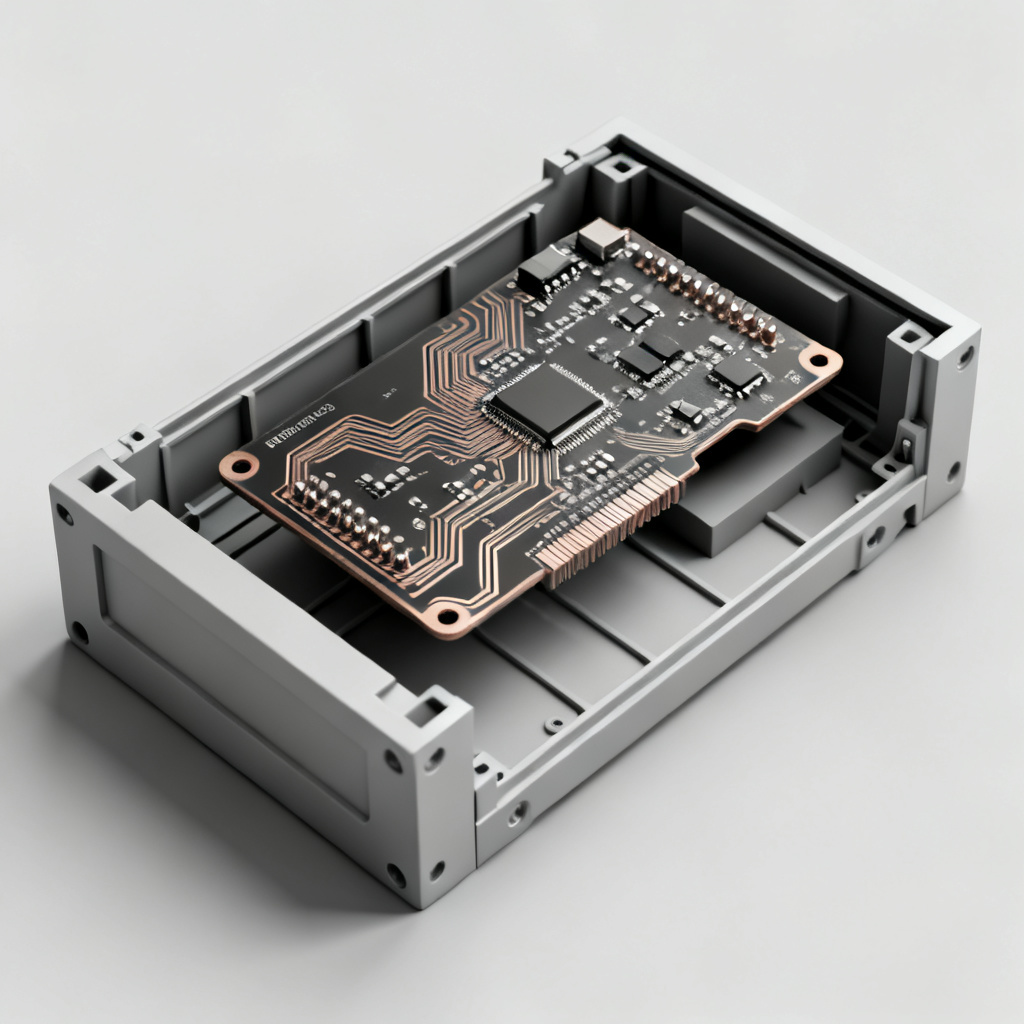
Key Strengths of Autodesk Eagle
- Seamless ECAD-MCAD Integration: This is Eagle’s single greatest advantage. When used within Fusion 360, the schematic and PCB layout are directly linked to the 3D mechanical model. You can see the board inside the enclosure, route cables, and perform mechanical analysis—all within one environment. This eliminates the “works in ECAD, doesn’t fit in MCAD” problem.
- User-Friendly Interface: Eagle is known for its intuitive, easy-to-learn interface. The schematic editor and layout tool are straightforward. The “Auto-router” (though not perfect) provides a quick starting point for beginners.
- Large, Active Community and Library: Eagle has a massive user base, particularly in the maker and startup communities. The “SparkFun” and “Adafruit” libraries are widely used. The Autodesk Content Center provides a vast library of manufacturer-approved components.
- Cloud-Based Collaboration: Fusion 360 with Eagle is cloud-native. Teams can share designs, manage versions, and collaborate in real-time from anywhere. This is excellent for distributed teams.
- Cost-Effective for Fusion 360 Users: If you already have a Fusion 360 subscription for mechanical design, the Eagle EDA features are included at no extra cost. This makes it the most cost-effective option for companies using the Autodesk ecosystem.
- Built-in Manufacturing Support: Eagle includes a “Manufacturing Output” panel that guides you through generating Gerber files. It also offers direct integration with Autodesk’s manufacturing partner network for quick-turn prototyping.
Who Should Use Autodesk Eagle (Fusion 360)?
- Startups and small businesses that need both mechanical and electrical design in one tool.
- Engineers who prioritize a smooth ECAD-MCAD workflow (e.g., designing a board that fits inside a specific custom enclosure).
- Hobbyists and educators who want a powerful, affordable tool with a gentle learning curve.
- Teams already using Autodesk products (Fusion 360, Inventor) who want to add PCB design capabilities.
Potential Drawbacks of Autodesk Eagle
- Subscription Model: Unlike KiCad (free) or Altium (perpetual license), Eagle is subscription-only. You must pay annually or monthly to keep using it.
- Feature Limitations for Complex Designs: Eagle is excellent for 2-4 layer boards and moderate complexity. It struggles with very high layer counts (16+), complex BGA routing, and advanced signal integrity analysis.
- Library Management Can Be Messy: While the community library is large, it can be inconsistent. Managing custom libraries and ensuring they are synchronized with the schematic can be problematic.
- Less Powerful Simulation: Eagle’s simulation capabilities are basic compared to PSpice (Cadence) or ngspice (KiCad). It is not suitable for advanced analog or high-speed simulation.
PCB EDA Tools Guide: Head-to-Head Comparison Table
| PCB EDA Tools Guide Feature | Altium Designer | KiCad | Cadence (OrCAD/Allegro) | Autodesk Eagle (Fusion 360) |
|---|---|---|---|---|
| License Cost | High (Perpetual + Annual) | Free (Open Source) | Very High (Perpetual + Annual) | Medium (Subscription) |
| Learning Curve | Moderate | Moderate to Steep | Very Steep | Low to Moderate |
| Best for Layer Count | 2-24+ layers | 2-16+ layers | 2-40+ layers | 2-8 layers |
| Signal Integrity Analysis | Good (Integrated SI) | Basic (ngspice) | Excellent (Sigrity, PSpice) | Basic |
| ECAD-MCAD Integration | Excellent (3D viewer + Step) | Good (Step import/export) | Excellent (Live with Creo/SW) | Best (Native Fusion 360) |
| Supply Chain Integration | Excellent (ActiveBOM) | Manual (via scripts/plugins) | Good (via integration) | Good (Autodesk network) |
| Team Collaboration | Good (Vault) | Good (Git integration) | Excellent (Concurrent layout) | Good (Cloud-based) |
| Manufacturing Outputs | Gerber X2, ODB++, IPC-2581 | Gerber X2, ODB++, IPC-2581 | Gerber X2, ODB++, IPC-2581 | Gerber, ODB++ |
| Best for B2B Manufacturing | Excellent (DFM, BOM, Outputs) | Very Good (with careful setup) | Excellent (Enterprise DFM) | Good (for simple boards) |
PCB EDA Tools Guide: How to Choose the Right Tool for Your PCB Production Needs
Your choice should not be based on features alone, but on your specific business context. Here is a decision framework for B2B PCB buyers:
1. High-Speed, Multi-Layer Design (e.g., 10-layer server board, FPGA carrier)
Choose Cadence (Allegro) or Altium Designer. You need the simulation accuracy (Cadence) or the unified workflow with excellent DFM (Altium). The cost is justified by reduced prototype iterations and guaranteed first-pass success.
2. Startup or SME with Tight Budget (e.g., 4-layer IoT device)
Choose KiCad. It is free, powerful, and has a massive library. The lack of cost allows you to invest more in prototyping. Ensure you have a clear DFM checklist for your manufacturer.
3. Product Requiring Close Mechanical Integration (e.g., board as structural part of handheld device)
Choose Autodesk Eagle (Fusion 360). The native ECAD-MCAD integration is unmatched. You can design the board and the enclosure simultaneously, avoiding expensive mechanical re-spins.
4. Large Enterprise with Dedicated Team (e.g., telecom base station)
Choose Cadence (Allegro). It is the only tool that scales to the largest teams and the most complex designs. The constraint management system is the most robust.
5. Contract Manufacturer (CM) or PCB Fabrication House
We recommend Altium Designer and KiCad as the most common formats we receive. However, we accept all four. We strongly advise using IPC-2581 output format for the most reliable data transfer, regardless of your tool.
PCB EDA Tools Guide: Conclusion
Selecting the right platform from this PCB EDA Tools Guide Altium KiCad Cadence Eagle matrix depends entirely on your project’s complexity, your team’s size, and your budget constraints. Altium Designer offers the best balance of power and usability for professional teams, while KiCad stands as the undisputed champion of open-source design. Cadence remains the ultimate weapon for high-speed, enterprise-level complexity, and Autodesk Eagle provides the most accessible bridge to mechanical environments.
Regardless of which tool you choose, the most important step is Design for Manufacturability (DFM). Always generate your fabrication outputs (Gerber, drill, and netlist) using the latest standards. Provide a clear stackup drawing. And most importantly, communicate with your PCB manufacturer early in the design process.
At [Your Company Name], we specialize in manufacturing PCBs designed in all these tools. We provide free DFM feedback to ensure your design is optimized for our processes, reducing your time-to-market and total cost.
PCB EDA Tools Guide: Frequently Asked Questions
What is the best PCB EDA tools guide for a beginner?
For beginners, Autodesk Eagle (Fusion 360) offers the most user-friendly interface, while KiCad provides a free and powerful alternative with a growing community. This PCB EDA tools guide recommends starting with Eagle for its gentle learning curve.
Which PCB EDA tool is best for high-speed design?
Cadence (OrCAD/Allegro) is the industry leader for high-speed design, offering unmatched signal integrity analysis. Altium Designer is also a strong contender with its integrated SI tools. This PCB EDA tools guide highlights Cadence for the most demanding high-speed projects.
Can I use KiCad for professional PCB manufacturing?
Yes, KiCad is fully capable of producing professional-grade outputs for manufacturing. Many contract manufacturers accept KiCad files. This PCB EDA tools guide confirms KiCad’s suitability for professional use with careful DFM setup.
Is Altium Designer worth the cost for a small business?
Altium Designer is a significant investment, but its unified workflow, ActiveBOM, and advanced routing features can save time and reduce errors for complex designs. For simple boards, KiCad or Eagle may be more cost-effective. This PCB EDA tools guide suggests evaluating your project complexity before investing.
What is the difference between Or CAD and Allegro?
OrCAD is Cadence’s mid-range tool for smaller teams, while Allegro is the flagship enterprise solution with advanced features for large-scale, high-speed designs. This PCB EDA tools guide clarifies that OrCAD is suitable for moderate complexity, while Allegro handles the most demanding applications.