Thick Copper Materials Foil Types and Stackup
For high-power PCB designs, Thick Copper Materials Foil Types and Stackup (≥3 oz) are essential for managing current and heat. This guide covers foil types and stackup architecture to ensure reliable manufacturing. Whether you need electrodeposited (ED) foil or rolled annealed (RA) foil, understanding your options is critical for success.
Thick Copper Foil Types Explained
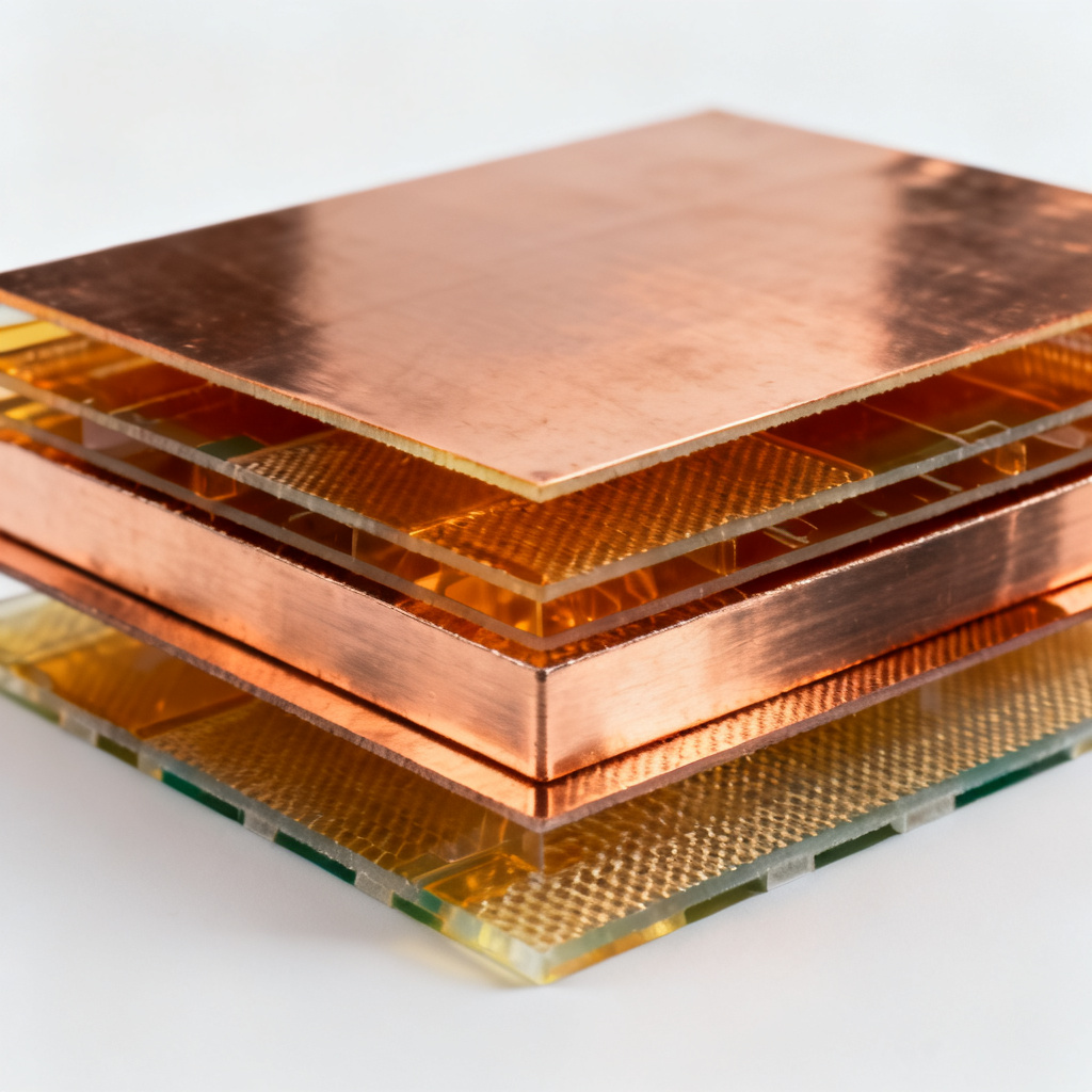
The selection of thick copper materials begins with foil type. Each variant offers distinct properties for different applications.
Electrodeposited (ED) Copper Foil
ED foil is the most common thick copper material for standard high-current boards. It offers high tensile strength (40,000–60,000 psi) but lower elongation (3–10%). The matte side provides excellent prepreg adhesion. For 3 oz to 6 oz designs, ED foil is cost-effective and reliable.
Rolled Annealed (RA) Copper Foil
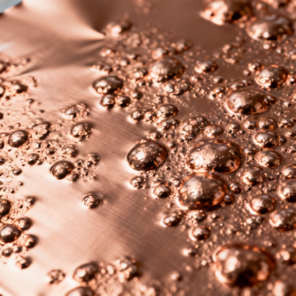
RA foil provides superior ductility (20–45% elongation), making it ideal for flexible circuits and extreme thermal cycling. Its smooth surface minimizes signal loss in high-frequency thick copper materials. However, RA foil is more expensive and requires special etching processes.
High-Ductility (HD) Copper Foil
HD foil bridges the gap between ED and RA. With 10–20% elongation, it offers improved thermal cycling performance without the full cost of RA. This thick copper material is popular for multi-layer automotive power electronics.
| Foil Type | Elongation (RT) | Best Application |
|---|---|---|
| ED Foil | 3–10% | Standard high-current boards |
| RA Foil | 20–45% | Flex, high-thermal-cycle designs |
| HD Foil | 10–20% | Multi-layer automotive power |
Thick Copper Stackup Design Principles
Designing a stackup with thick copper materials requires careful attention to copper-to-dielectric ratios. Prepreg thickness should be at least 1.5–2 times the copper thickness to prevent voids.
Symmetrical Stackup (Recommended)
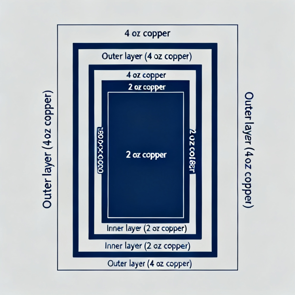
For multi-layer boards, symmetry is mandatory. An unbalanced stackup (e.g., 6 oz on one side, 2 oz on the other) causes severe warpage. A symmetrical 4-layer example: top and bottom layers use 4 oz copper, with 2 oz on inner layers and 2x 7628 prepreg between.
Asymmetrical Stackup Mitigations
If asymmetry is unavoidable, use copper thieving (dummy copper) on lighter layers to balance thermal mass. Sequential lamination can also help manage extreme imbalances in thick copper materials.
Via Design for Thick Copper PCBs
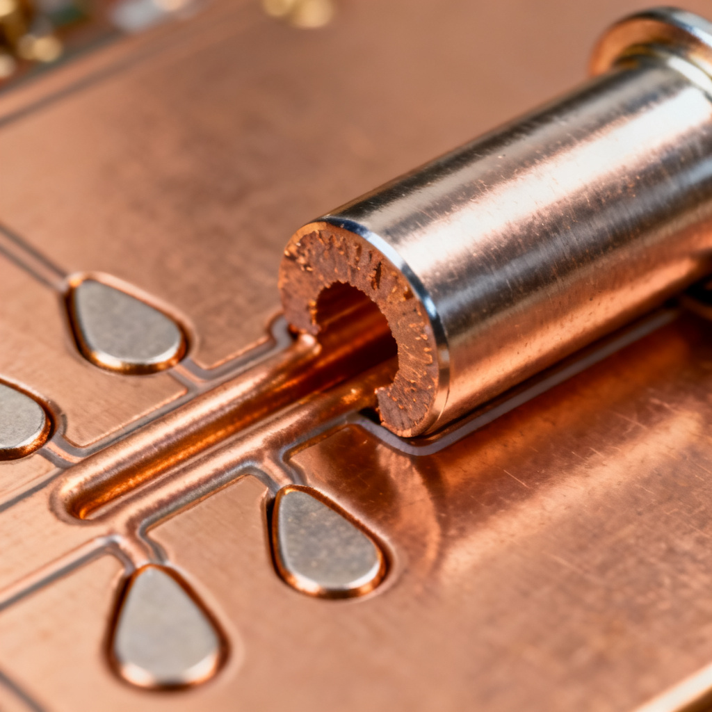
Vias in thick copper materials require larger diameters (aspect ratio ≤ 8:1) to ensure reliable plating. Tear-drop pad connections are essential to prevent barrel cracking. For via tenting, plugging with epoxy is more reliable than standard solder mask.
Trace and Spacing Rules
For 4 oz copper, minimum trace width is 8–10 mils; for 6 oz, 12–15 mils. Spacing should equal or exceed copper thickness. All corners should be chamfered or rounded to reduce stress concentration in thick copper materials.
Manufacturing Process Considerations
Etching thick copper materials requires longer times, leading to undercut. Use a compensation factor of 1.5–2x copper thickness. Lamination pressure should be 300–400 psi, and drilling may require multiple hits to achieve clean hole walls.
Frequently Asked Questions
What is the best thick copper material for high-current designs?
For standard high-current boards, ED foil (3–6 oz) is the most cost-effective thick copper material. For extreme thermal cycling, consider RA or HD foil.
How do I choose between ED and RA foil?
ED foil offers lower cost and good strength; RA foil provides superior ductility. Your choice depends on thermal cycling requirements and budget for thick copper materials.
Can I use thick copper materials in multi-layer boards?
Yes, but symmetrical stackups are critical. Use copper thieving if asymmetry is required. Prepreg thickness must exceed copper thickness to avoid voids.