Aerospace Defense PCB Guide MIL PRF 31032 AS9100 HDI
The Aerospace & Defense PCB is the backbone of mission-critical systems, from satellite communications and radar to avionics and missile guidance. This comprehensive Aerospace & Defense PCB Guide covers MIL‑PRF‑31032, AS9100, and HDI technology to help you design and manufacture boards that withstand extreme conditions.
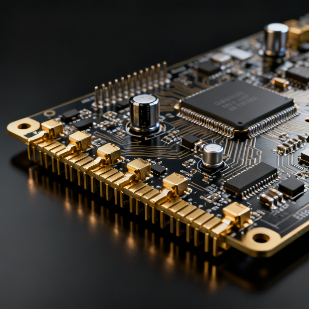
Key Standards: MIL‑PRF‑31032 & AS9100 for Aerospace & Defense PCB
MIL‑PRF‑31032: The Gold Standard for Military PCBs
What is MIL‑PRF‑31032? MIL‑PRF‑31032 is the U.S. Department of Defense’s performance specification for rigid, flexible, and rigid‑flex printed boards, replacing MIL‑P‑55110. This Aerospace & Defense PCB standard defines electrical, mechanical, and environmental performance requirements for military and aerospace systems.
Key Requirements:
- Material Qualification: All base materials (e.g., FR‑4, polyimide, PTFE) must be qualified to MIL‑S‑13949 or equivalent.
- Testing and Inspection: Mandates rigorous testing including electrical (continuity, insulation resistance, dielectric withstanding voltage), mechanical (peel strength, solderability, thermal stress), and environmental (moisture resistance, thermal cycling, vibration, shock).
- Traceability: Every board must be traceable from raw material to finished product, with lot control and serialization.
- Quality Conformance: Requires a Quality Conformance Inspection (QCI) plan with periodic testing of coupons and production boards.
Why MIL‑PRF‑31032 Matters for Aerospace & Defense PCB: Ensures reliability, interchangeability, and compliance with government contracts.
AS9100: The Aerospace Quality Management System
What is AS9100? AS9100 is the internationally recognized quality management system (QMS) standard for the aerospace industry, based on ISO 9001 with additional requirements for aviation, space, and defense. AS9100 certification is often a prerequisite for suppliers to major primes like Boeing, Airbus, Lockheed Martin, and NASA.
Key AS9100 Requirements for Aerospace & Defense PCB Manufacturers:
- Risk Management: Proactive identification and mitigation of risks throughout production.
- Configuration Management: Strict control over design changes, documentation, and product configuration.
- Product Traceability: Full traceability of materials, processes, and inspections from receipt to shipment.
- Special Processes: Control of plating, etching, soldering with documented procedures and operator certifications.
- Supplier Management: Rigorous assessment and monitoring of sub‑tier suppliers.
- Continuous Improvement: Implementation of corrective and preventive actions (CAPA) based on data analysis.
How AS9100 Complements MIL‑PRF‑31032: While MIL‑PRF‑31032 focuses on technical performance, AS9100 ensures the entire manufacturing process is managed with aerospace‑level quality.
HDI Technology in Aerospace & Defense PCB
What is HDI and Why is It Used?
Definition: HDI (High‑Density Interconnect) PCBs feature finer lines and spaces (≤ 100µm), smaller vias (≤ 150µm), and higher connection pad density than conventional PCBs. They use microvias (laser‑drilled), buried vias, and sequential lamination to achieve higher circuit density.
Why HDI is Critical for Aerospace & Defense PCB:
- Miniaturization: Modern systems demand smaller, lighter electronics. HDI allows more functionality in a smaller footprint, critical for UAVs, satellites, and portable equipment.
- Signal Integrity: Shorter signal paths and reduced parasitic capacitance/inductance improve high‑frequency performance (e.g., radar, communications).
- Thermal Management: HDI designs can incorporate thermal vias and copper‑filled microvias to dissipate heat more effectively.
- Reliability: Microvias, when properly designed and manufactured, offer superior reliability under thermal cycling compared to through‑hole vias.
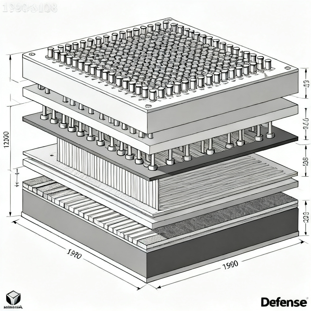
HDI Stackup and Design Considerations for Defense
Common HDI Stackups: 1+N+1, 2+N+2, i+N+i (any number of HDI layers on each side of a core).
Design Rules for Aerospace HDI:
- Microvia Aspect Ratio: Typically 1:1 (depth:diameter) for reliability. Maximum 1:1.5 for advanced applications.
- Via Fill: Microvias must be filled with conductive or non‑conductive material to prevent voids. Copper‑filled vias are preferred for high‑current and thermal applications.
- Minimum Trace/Spacing: 75µm/75µm (3/3 mil) common; advanced designs can achieve 50µm/50µm (2/2 mil).
- Dielectric Thickness: Thin dielectric layers (e.g., 50‑100µm) reduce via depth and improve signal integrity.
Material Selection for HDI in Defense:
- High‑Tg FR‑4: For less demanding environments (Tg > 170°C).
- Polyimide: For extreme temperature ranges (-55°C to +260°C) and high reliability.
- PTFE (Teflon): For high‑frequency applications (e.g., radar, antennas) due to low dielectric constant and low loss tangent.
- Ceramic‑Filled Laminates: For improved thermal conductivity and CTE matching.
Material Selection for Aerospace & Defense PCB
Key Material Properties
Glass Transition Temperature (Tg): For aerospace, Tg > 170°C is typical; polyimide offers Tg > 260°C.
Coefficient of Thermal Expansion (CTE): Must match copper and components to prevent solder joint failure. Low CTE materials (e.g., polyimide, ceramic‑filled laminates) are preferred.
Dielectric Constant (Dk) and Dissipation Factor (Df): For high‑frequency boards, low Dk (e.g., 3.0‑3.5) and low Df (e.g., < 0.005) are critical to minimize signal loss.
Thermal Conductivity: High thermal conductivity (e.g., > 1.0 W/mK) helps dissipate heat from high‑power components.
Moisture Absorption: Low moisture absorption (< 0.5%) prevents delamination and electrical failures in humid environments.
Common Materials and Their Applications
| Aerospace & Defense PCB Material | Tg (°C) | CTE (ppm/°C) | Dk @ 1GHz | Application |
|---|---|---|---|---|
| Standard FR‑4 | 130‑140 | 14‑16 | 4.5‑4.8 | Commercial, non‑critical |
| High‑Tg FR‑4 | 170‑180 | 12‑14 | 4.2‑4.5 | Avionics, ground support |
| Polyimide | 250‑260 | 12‑14 | 3.8‑4.2 | Military, space, high‑temp |
| PTFE/Woven Glass | 280+ | 8‑10 | 2.2‑2.5 | Radar, antennas, RF |
| Ceramic‑Filled PTFE | 280+ | 6‑8 | 3.0‑3.5 | High‑power RF, thermal management |
Special Note on Polyimide: Polyimide is the most common material for military PCBs due to its high Tg, low CTE, and excellent chemical resistance. However, it requires specialized processing (higher lamination pressure, slower drilling).
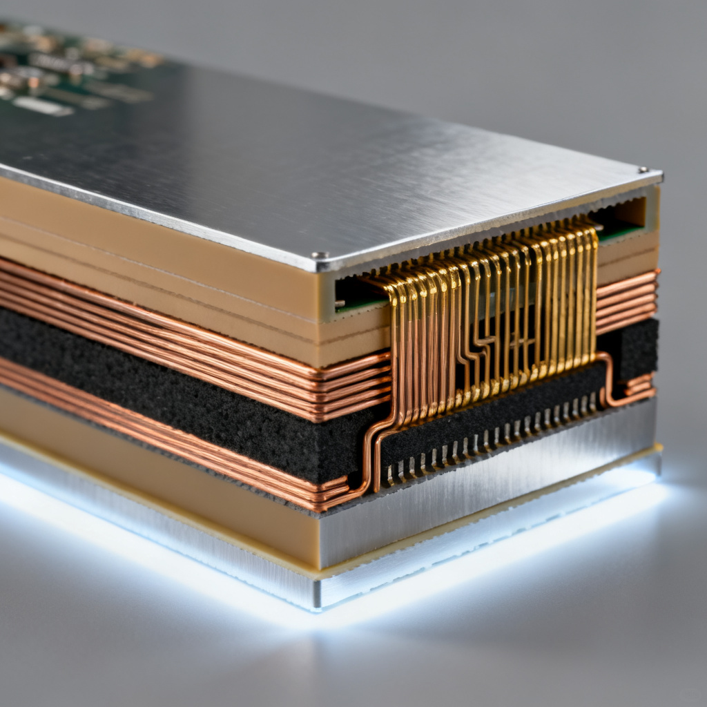
Design Guidelines for High‑Reliability Aerospace & Defense PCB
General Design Rules
- Minimum Trace Width/Spacing: 0.15mm (6 mil) for standard, 0.075mm (3 mil) for HDI.
- Minimum Annular Ring: 0.15mm (6 mil) for outer layers, 0.1mm (4 mil) for inner layers.
- Minimum Hole Size: 0.3mm (12 mil) for mechanical drills, 0.1mm (4 mil) for laser drills.
- Copper Weight: 1 oz (35µm) standard; heavier copper (2‑4 oz) for high‑current power planes.
- Solder Mask: Type III or Type IV liquid photoimageable solder mask (LPSM) for fine‑pitch components.
Thermal Management Design
Use Thermal Vias: Place arrays of vias under high‑power components to conduct heat to inner ground planes.
Copper Pour: Include large copper areas on outer layers for heat spreading.
Thermal Relief Pads: Use thermal reliefs on pads connected to large copper planes to facilitate soldering.
Consider Metal Core PCBs (MCPCB): For extreme thermal requirements, use aluminum or copper cores.
Signal Integrity and EMI Control
Controlled Impedance: Design transmission lines (microstrip, stripline) with controlled impedance (e.g., 50Ω, 75Ω) for high‑speed signals.
Ground Planes: Use continuous ground planes to reduce EMI and provide return paths.
Decoupling Capacitors: Place capacitors close to IC power pins to filter noise.
Shielding: Use copper shielding cans or conductive gaskets for sensitive RF sections.
Manufacturing Considerations
Panel Utilization: Optimize panel size to minimize waste and reduce cost.
Tolerances: Specify tight tolerances for critical dimensions (e.g., ±0.05mm for hole location, ±10% for impedance).
Testing: Include test coupons on the panel for electrical and mechanical testing per MIL‑PRF‑31032.
Documentation: Provide complete fabrication drawings including stackup, material specifications, and test requirements.
Manufacturing Process for Aerospace & Defense PCB
Process Overview
- Material Receipt and Inspection: All materials verified against MIL‑S‑13949 or equivalent.
- Inner Layer Imaging and Etching: Laser direct imaging (LDI) for fine lines; controlled etching for uniform copper thickness.
- Lamination: Sequential lamination for HDI; precise pressure and temperature profiles for polyimide.
- Drilling: Mechanical drilling for through‑holes; laser drilling (CO2 or UV) for microvias.
- Plating: Electroless copper followed by electrolytic copper plating; copper filling for microvias.
- Outer Layer Imaging and Etching: Same as inner layers, with additional registration accuracy.
- Solder Mask Application: Liquid photoimageable solder mask (LPSM) applied and cured.
- Surface Finish: ENIG (Electroless Nickel Immersion Gold) or HASL (Hot Air Solder Leveling) for solderability; ENIG preferred for fine‑pitch.
- Electrical Testing: Flying probe or fixture‑based testing for continuity and isolation.
- Final Inspection: Visual inspection, dimensional verification, and coupon testing per MIL‑PRF‑31032.
Quality Control and Testing
In‑Process Inspection: Automated optical inspection (AOI) at every critical step.
Coupon Testing: Test coupons from each panel undergo thermal stress (solder float at 288°C for 10 seconds), peel strength measurement, dielectric withstanding voltage (DWV), and insulation resistance.
Final Quality Check: 100% electrical testing, visual inspection per IPC‑A‑600 Class 3, and dimensional verification.
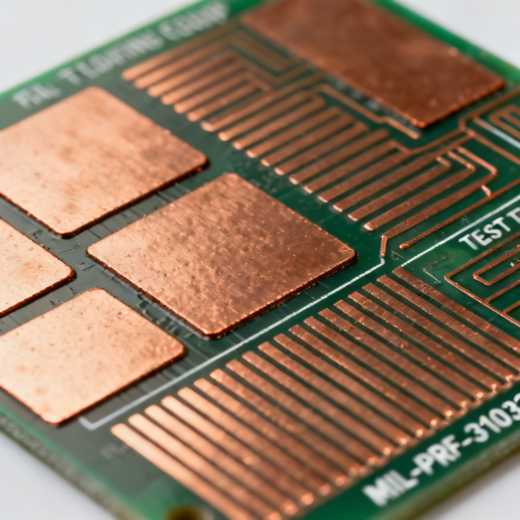
Common Challenges and Solutions in Aerospace & Defense PCB Manufacturing
Challenge: High‑Temperature Materials (Polyimide)
Solution: Use specialized drilling parameters (higher spindle speed, slower feed), controlled lamination cycles, and plasma desmear to ensure clean holes and strong interlayer adhesion.
Challenge: HDI Microvia Reliability
Solution: Ensure proper via filling (copper or non‑conductive), maintain aspect ratio ≤ 1:1, and perform thermal cycling testing to validate reliability.
Challenge: Achieving Controlled Impedance
Solution: Use precise dielectric thickness control, consistent copper weight, and impedance testing on every panel. Design for manufacturing (DFM) feedback helps adjust stackup.
Challenge: Meeting Traceability Requirements
Solution: Implement a robust ERP/MES system that tracks every board from raw material to shipment. Use barcode or QR code serialization for individual boards.
Challenge: Cost vs. Performance Balance
Solution: For less critical applications, use High‑Tg FR‑4 instead of polyimide. For HDI, minimize the number of sequential lamination cycles. Always request a DFM review from your manufacturer.
How to Choose the Right Aerospace & Defense PCB Manufacturer
Key Criteria for Manufacturer Selection
- Certifications: Must hold AS9100 and be capable of MIL‑PRF‑31032 compliance. Look for ITAR registration if dealing with U.S. defense.
- Experience: Proven track record in aerospace and defense projects. Ask for case studies or references.
- Capabilities: In‑house HDI production, laser drilling, copper filling, sequential lamination, and heavy copper.
- Testing: In‑house electrical testing, impedance testing, and thermal cycling capabilities.
- Quality System: Robust quality management with CAPA, FMEA, and SPC.
- Lead Time: Ability to meet tight deadlines for prototypes and production runs.
- Customer Support: Dedicated engineering support for DFM and design optimization.
Questions to Ask Potential Manufacturers
- Are you AS9100 certified? Can you provide proof?
- Do you have experience with MIL‑PRF‑31032? Can you share a qualification test report?
- What is your maximum layer count for HDI?
- Can you handle polyimide and PTFE materials?
- What is your typical lead time for prototype and production orders?
- Do you offer design for manufacturing (DFM) feedback?
FAQ: Aerospace & Defense PCB Guide
What is the difference between MIL‑PRF‑31032 and MIL‑P‑55110?
MIL‑PRF‑31032 is the current performance specification for Aerospace & Defense PCB, replacing MIL‑P‑55110. It includes more rigorous testing and traceability requirements.
Why is AS9100 important for Aerospace & Defense PCB manufacturers?
AS9100 ensures a quality management system that meets aerospace industry standards, which is often required by major primes for Aerospace & Defense PCB supply.
What materials are best for high‑frequency Aerospace & Defense PCB?
PTFE and ceramic‑filled laminates are preferred for high‑frequency Aerospace & Defense PCB due to low Dk and low loss.
How does HDI benefit Aerospace & Defense PCB design?
HDI enables miniaturization, improved signal integrity, and better thermal management for Aerospace & Defense PCB in compact systems.
What testing is required for MIL‑PRF‑31032 compliant Aerospace & Defense PCB?
Testing includes electrical (continuity, insulation resistance), mechanical (peel strength, thermal stress), and environmental (moisture resistance, thermal cycling) tests.
Conclusion: Building Trust Through Expertise and Compliance
Aerospace & Defense PCB demand the highest levels of reliability, traceability, and performance. By understanding MIL‑PRF‑31032, AS9100, and HDI technology, you can ensure your boards meet mission‑critical requirements. At [Your Company Name], we combine decades of experience with AS9100‑certified manufacturing and MIL‑PRF‑31032 compliance to deliver Aerospace & Defense PCB that exceed expectations. Contact our engineering team today for a free DFM review and competitive quote.