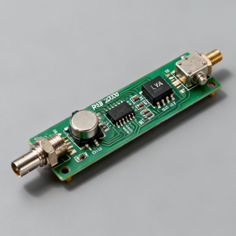
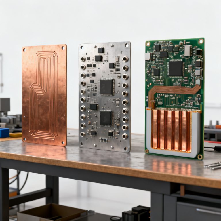
PCB Principles & Fundamentals: Signal Integrity, EMI, Thermal Management
When studying PCB Principles Fundamentals Signal Integrity EMI Thermal Management, these three components cannot be separated.Mastering PCB Principles Fundamentals: Signal Integrity, EMI, Thermal Management is essential for any modern electronic product. These three interconnected disciplines determine whether a board will function reliably at high speeds, pass regulatory compliance, and survive thermal stress.
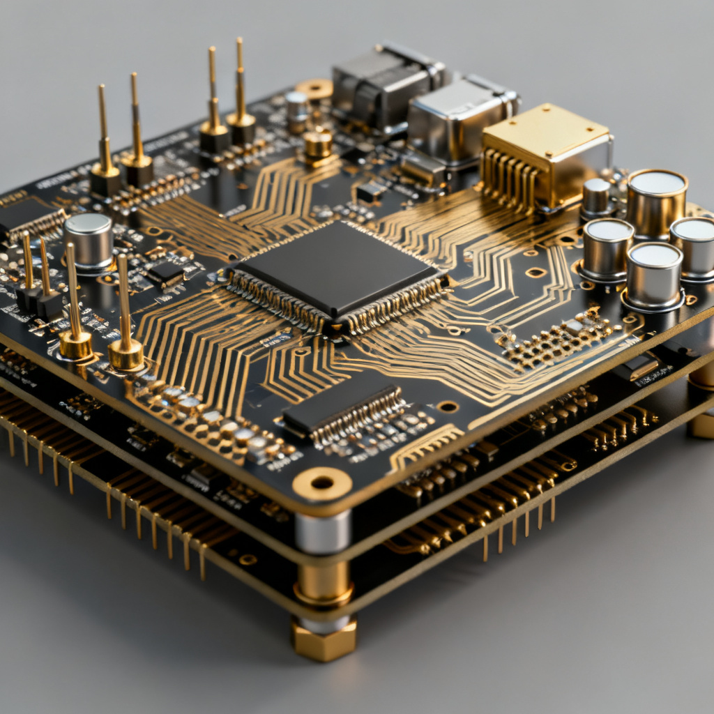
Signal Integrity: Preserving the Quality of Electrical Signals
Signal Integrity is the art and science of ensuring that an electrical signal travels from the driver to the receiver with minimal distortion, delay, or loss. In high-speed digital design, a signal that fails to maintain its integrity can cause data errors, system crashes, or complete failure.
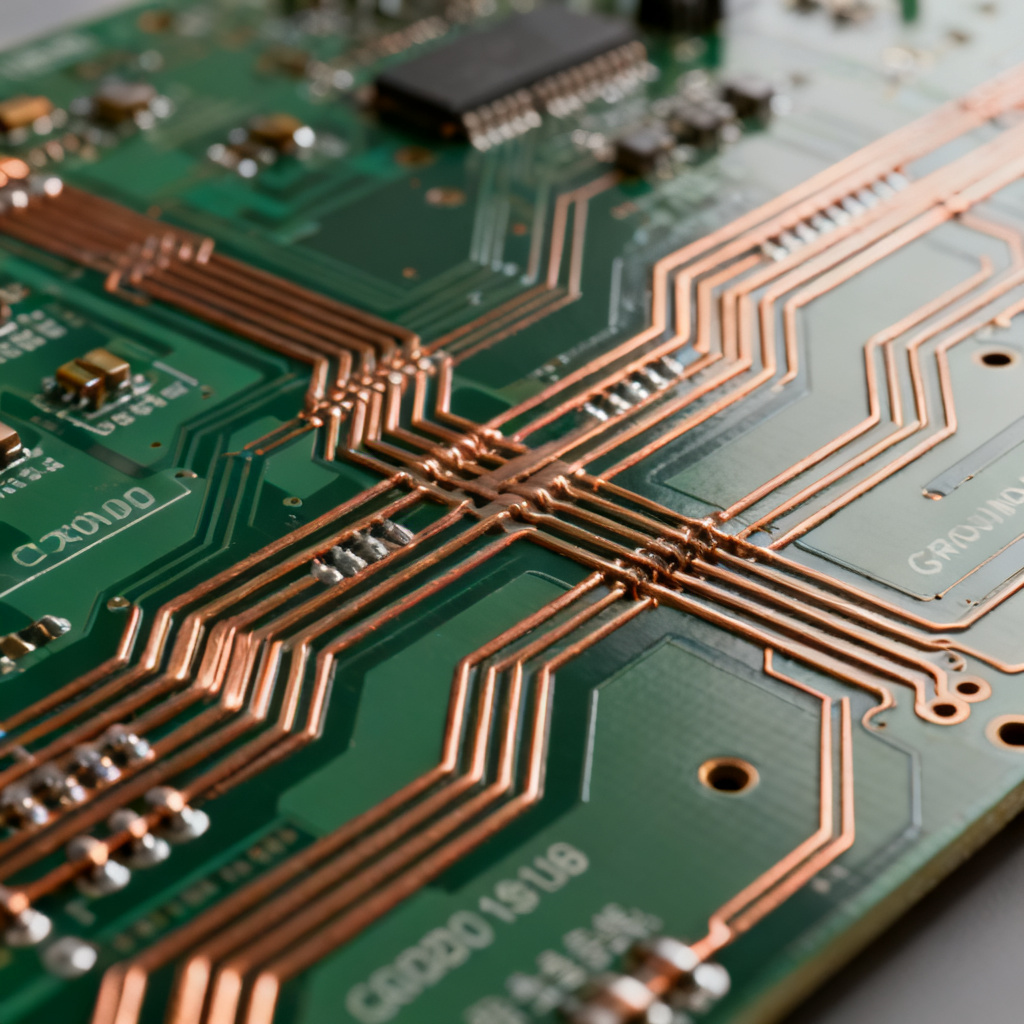
Impedance Control: The Foundation of Signal Integrity
Impedance is the opposition a circuit presents to the flow of an alternating current (AC) signal. In a PCB trace, it is a function of the trace width, copper thickness, dielectric material, and the distance to the reference plane (ground or power plane). To prevent signal reflections, the impedance of the transmission line must match the impedance of the driver, the load, and any connectors. The most common standard is 50 Ohms for single-ended signals and 100 Ohms differential for differential pairs (e.g., USB, HDMI, Ethernet). Any impedance discontinuity (a sudden change in trace width, a via, or a stub) will cause a portion of the signal to reflect back toward the source, creating ringing and overshoot.
Reflections and Terminations in Signal Integrity
When a signal encounters a mismatch, a reflected wave travels back. This can add to or subtract from the original signal, causing logic-level errors. Proper termination is critical. Common methods include series termination (a resistor placed near the driver to match the source impedance to the trace impedance), parallel termination (a resistor placed near the receiver to ground or Vcc to match the load impedance), and AC termination (a resistor and capacitor in series to ground, useful for reducing DC power consumption).
Crosstalk: The Unwanted Coupling Affecting Signal Integrity
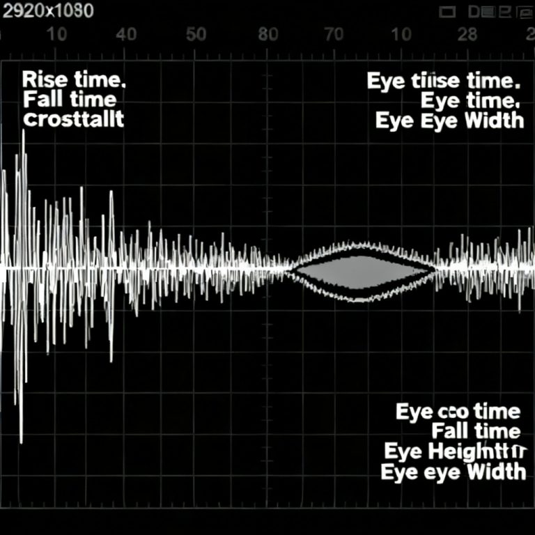
Crosstalk is the electromagnetic coupling of energy from one signal trace (the aggressor) to an adjacent trace (the victim). It is the primary cause of noise in tightly packed digital circuits. Types of crosstalk include forward crosstalk (travels in the same direction as the aggressor signal) and backward (near-end) crosstalk (travels back toward the source). Mitigation strategies include increasing spacing (a general rule is to keep trace-to-trace spacing at least 3 times the trace width, known as the 3W rule), using guard traces (a grounded trace placed between two signal traces, stitched to the ground plane with vias at regular intervals), reducing parallel run length, and using layer stack-up (stripline routing, which inherently provides better isolation than microstrip).
High-Speed Design Techniques for Signal Integrity
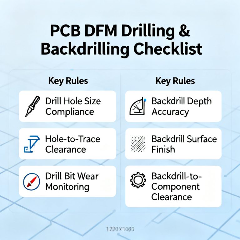
Trace routing best practices include avoiding 90-degree corners (use 45-degree chamfers or curved traces), minimizing stubs (use back-drilling to remove unused via stubs), and routing differential pairs with equal length and constant spacing. A solid, unbroken reference plane (usually ground) directly beneath the signal trace is essential. It provides the return path for the signal current. If the return path is forced to detour around a split in the plane, it creates a large loop antenna, radiating EMI and degrading signal integrity. Never route a high-speed signal across a split in the ground plane. If a split is unavoidable, use stitching capacitors to bridge the gap.
EMI Control: Controlling Unwanted Radiation
EMI, also known as Radio Frequency Interference (RFI), is the disturbance generated by an electrical circuit that affects other circuits through electromagnetic induction, electrostatic coupling, or conduction. Effective EMI control is essential for passing regulatory compliance (e.g., FCC, CE) and ensuring reliable system operation.
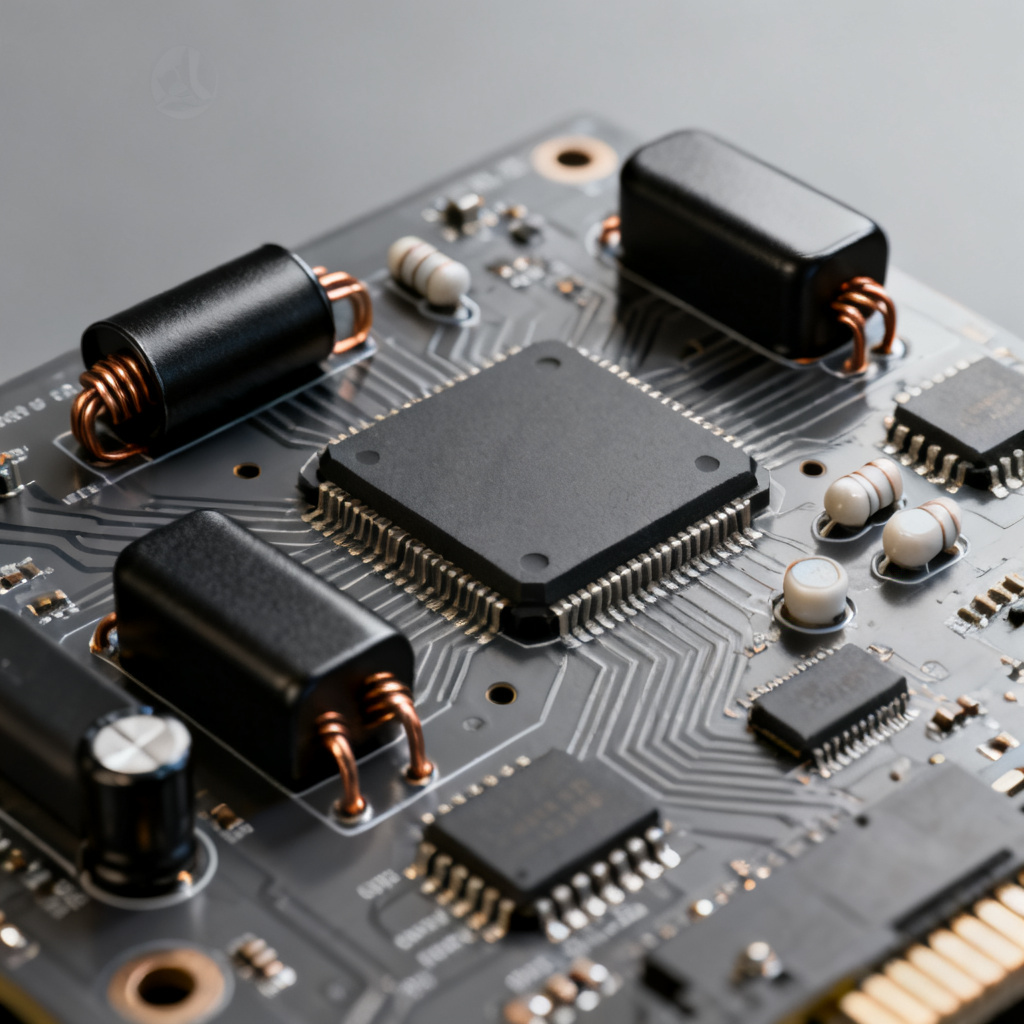
The Sources and Mechanisms of EMI
Common-mode noise (unwanted currents that flow in the same direction on both the signal trace and the ground plane) is the primary cause of radiated EMI, as it creates a large, efficient antenna. Most EMI problems originate from common-mode currents caused by ground bounce, poor decoupling, or unbalanced differential pairs. Radiated emissions escape the PCB through electromagnetic waves, while conducted emissions travel along power lines or other cables.
PCB Design Strategies for EMI Reduction
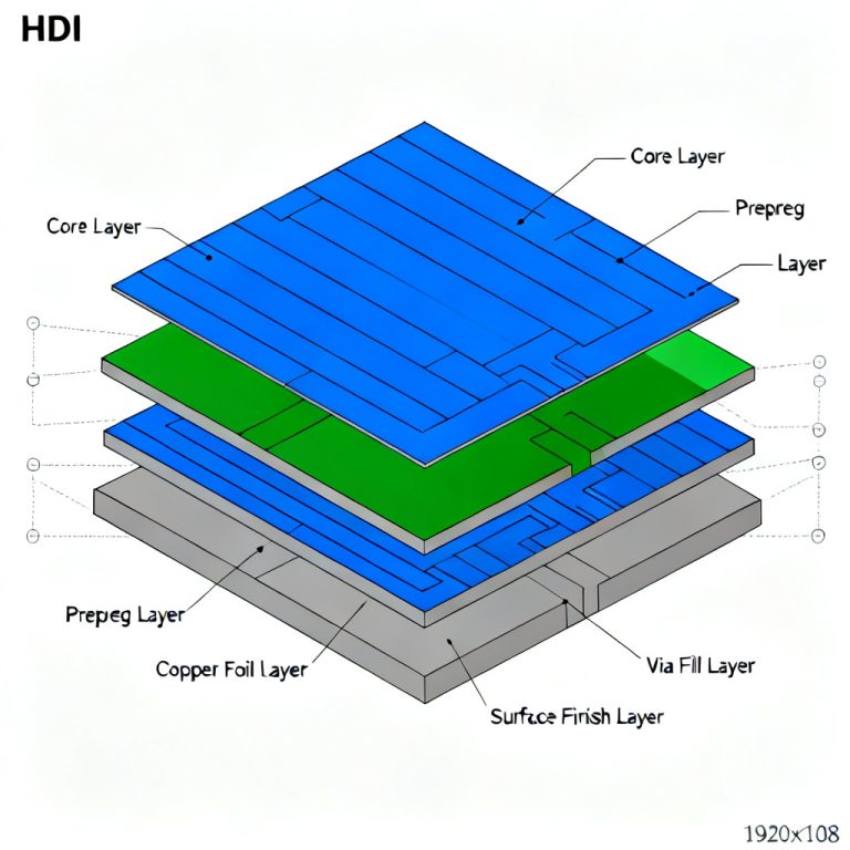
A 4-layer board (Signal-Ground-Power-Signal) is significantly better than a 2-layer board for EMI control. The internal ground and power planes create a low-inductance power distribution network and provide a shield. For high-density designs, a 6-layer stack-up (e.g., Signal-Ground-Signal-Signal-Power-Signal) offers optimal routing flexibility while maintaining two dedicated ground planes. Always place a ground plane adjacent to the top and bottom signal layers.
Decoupling capacitors provide a local reservoir of charge for high-speed ICs, preventing voltage droops and reducing the noise injected into the power plane. Place the smallest value capacitor as close as possible to the power pin of the IC. Use a range of capacitor values (e.g., 100 µF, 10 µF, 0.1 µF, 0.01 µF) to cover a broad frequency spectrum.
Board-level shields (metal cans) placed over sensitive or noisy sections of the PCB must be connected to the ground plane with a low-impedance path (many vias around the perimeter). Guard rings (a grounded copper ring) are most effective when placed on the top layer and stitched to the ground plane with vias.
Place common-mode chokes and ferrite beads on all I/O lines, with the filter placed as close to the connector as possible. Minimizing loop area is critical: provide a continuous, low-inductance return path for every signal and avoid routing signals over split planes.
Thermal Management: Keeping the Board Cool
Thermal Management is the process of controlling the temperature of components and the PCB itself to ensure reliable operation and prevent premature failure. Modern high-power ICs generate significant heat that must be dissipated.
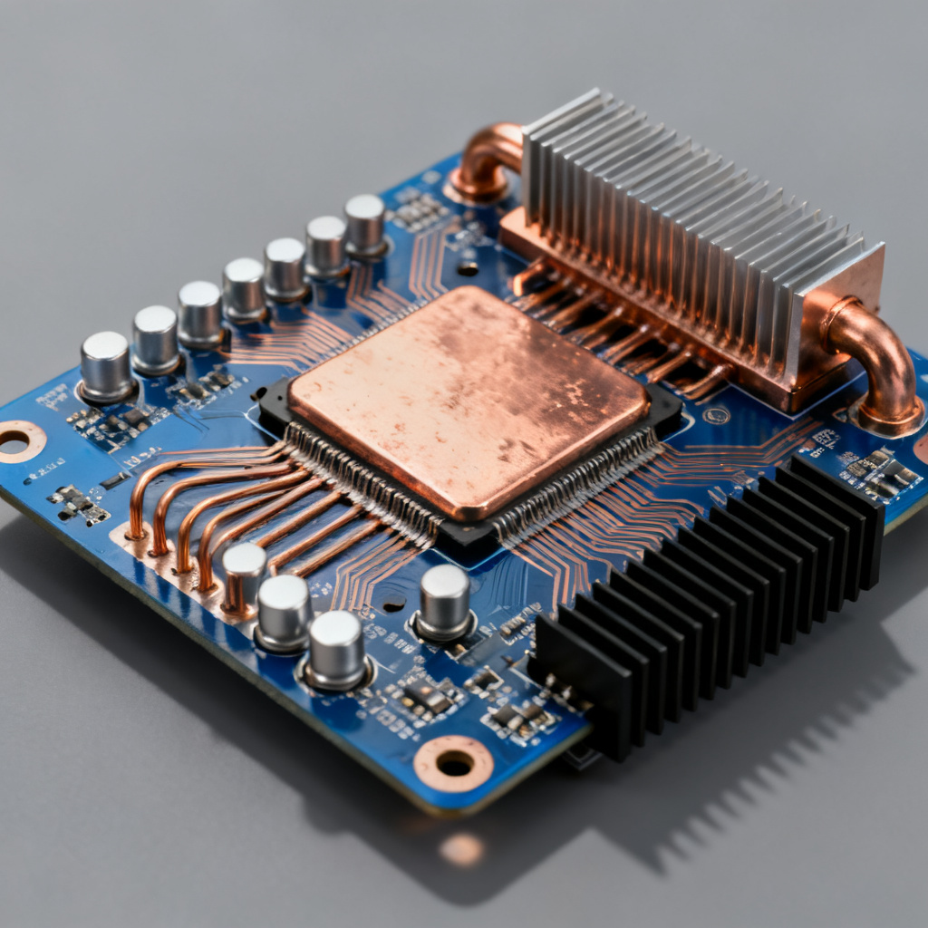
The Physics of Heat Transfer on a PCB
The three modes of heat transfer are conduction (heat transfer through solid materials, the primary method for moving heat from a component to the PCB), convection (heat transfer to a fluid, such as air, where forced convection using a fan is much more effective than natural convection), and radiation (heat transfer via electromagnetic waves, significant only at very high temperatures or in a vacuum). Thermal resistance (Theta-JA and Theta-JC) is a key parameter: Theta-JA measures the resistance from the semiconductor junction to the ambient air, while Theta-JC measures the resistance from the junction to the case.
PCB Design Techniques for Effective Heat Dissipation
For high-power components, connect the component’s thermal pad to a large copper pour on the top layer. Use a grid of small thermal vias (e.g., 0.3mm diameter) placed directly under the thermal pad to conduct heat from the top layer to the internal ground and power planes.
A 4-layer PCB can dissipate significantly more heat than a 2-layer board. Use solid copper pours on all unused areas of the board, connected to the ground net with thermal reliefs.
Place high-power components away from temperature-sensitive components. Do not block the natural airflow path; place tall components near the edge of the board or the exhaust of a fan. Attach heatsinks to the top of high-power ICs and use thermal pads or thermal paste to fill microscopic air gaps. For complex designs, use Computational Fluid Dynamics (CFD) software to model airflow and temperature distribution.
See more about PCB design: RF PCB Layout Guideline.
Interplay of Signal Integrity, EMI, and Thermal Management
These three principles are not independent; they are deeply interconnected. A thermal via can create an impedance discontinuity in a high-speed signal path if placed too close to the trace. A large copper pour used for heat spreading can create a return path discontinuity for a high-speed signal if it is not part of the ground plane. A heatsink attached to a fast-switching IC can act as an antenna, worsening EMI. Mastering PCB design requires a holistic approach, balancing the requirements of signal integrity, EMI control, and thermal management to create a robust, reliable, and manufacturable product.
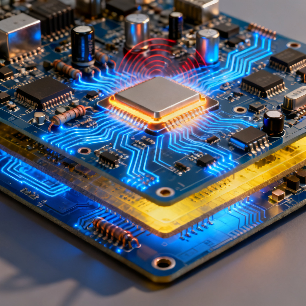
| Parameter | Signal Integrity Impact | EMI Impact | Thermal Management Impact |
|---|---|---|---|
| Impedance (50 Ohms) | Controls reflections | Reduces radiated emissions | Minimal direct impact |
| Trace Spacing (3W rule) | Reduces crosstalk | Reduces coupling | Allows airflow |
| Copper Pour Thickness | Provides return path | Provides shielding | Acts as heat spreader |
| Thermal Via Density | Can cause discontinuity | Can create antenna | Improves heat transfer |
Glossary of Key Terms
- Signal Integrity (SI): The ability of a signal to maintain its quality from source to destination.
- Electromagnetic Interference (EMI): Unwanted electromagnetic energy that disrupts circuit operation.
- Thermal Management: The process of controlling temperature to ensure component reliability.
- Impedance: The opposition a circuit presents to AC current flow, critical for signal integrity.
- Crosstalk: Unwanted coupling of energy between adjacent traces, degrading signal integrity.
- Common-Mode Noise: Unwanted currents flowing in the same direction, a primary source of EMI.
- Thermal Vias: Small vias used to conduct heat from components to internal copper planes.