SPI in SMT Assembly Optimizing PCB Quality
Discover how SPI in SMT Assembly Optimizing PCB Quality transforms modern electronics manufacturing. In the fast-paced world of production, quality control is paramount. We understand that the key to producing high-quality PCBs lies in the details of our SMT assembly process. One crucial step that often goes unnoticed but plays a vital role in ensuring PCB quality is Solder Paste Inspection or SPI。
Table of Contents
- Introduction to SPI in SMT Assembly
- The SPI Process Explained
- Benefits of Implementing SPI
- SPI Integration in the SMT Assembly Line
- Key Parameters Measured by SPI
- SPI Technology Advancements
- Interpreting SPI Data
- Best Practices for Effective SPI Implementation
- SPI’s Role in Industry 4.0 and Smart Manufacturing
- Case Study: SPI Implementation
- Future Trends in SPI Technology
- Conclusion
Introduction to SPI in SMT Assembly
What exactly is SPI in the SMT process?
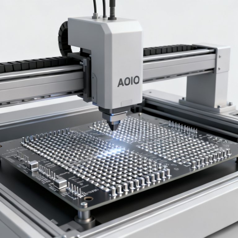
SPI, short for Solder Paste Inspection, is a critical quality control measure used in Surface Mount Technology (SMT) assembly. It’s an automated optical inspection technique that examines the solder paste deposits on a PCB before component placement. This inspection ensures that the right amount of solder paste is applied in the correct locations, setting the foundation for a successful SMT assembly.
The importance of SPI in SMT assembly cannot be overstated. As PCB designs become more complex and component sizes shrink, the margin for error in solder paste application becomes increasingly narrow. Even minor inconsistencies in solder paste volume, position, or shape can lead to significant defects in the final product. This is where SPI shines, acting as a gatekeeper to catch potential issues before they become costly problems.
At Sensormass, we’ve integrated advanced SPI systems into our SMT assembly lines to enhance our PCB manufacturing quality. By implementing SPI, we’re able to:
- Detect and correct solder paste printing errors early in the production process
- Ensure consistent solder joint quality across all PCBs
- Reduce defects related to insufficient or excess solder paste
- Minimize rework and improve overall production efficiency
SPI technology has evolved significantly over the years, from simple 2D imaging to sophisticated 3D measurement systems. These advancements have made SPI an indispensable tool in modern SMT assembly, capable of measuring solder paste volume, area, height, and position with incredible accuracy.
As we delve deeper into the world of SPI in SMT assembly, you’ll discover how this technology is revolutionizing PCB manufacturing. From its core principles to its impact on production quality, we’ll explore why SPI has become a cornerstone of quality assurance in the electronics industry.
Stay tuned as we unpack the intricacies of the SPI process, its benefits, and how it’s shaping the future of PCB assembly and beyond. Whether you’re a seasoned engineer or new to the world of PCB manufacturing, understanding SPI is key to appreciating the level of precision and care that goes into every board we produce.
The SPI Process Explained
At Sensormass, we believe that understanding the SPI process is crucial for appreciating the quality assurance measures we implement in our SMT assembly line. Let’s dive into the heart of SPI technology and explore how it works to ensure your PCBs meet the highest standards.
Key Components of an SPI System
A typical SPI system consists of several essential components working in harmony:
- Illumination System: High-quality LED lights that provide consistent, even lighting for accurate inspection.
- Camera System: High-resolution cameras capture detailed images of the solder paste deposits.
- Optical System: Lenses and mirrors that focus and direct light for optimal image capture.
- Motion Control System: Precise motors and stages that move the PCB or camera for comprehensive coverage.
- Image Processing Software: Advanced algorithms that analyze the captured images and compare them to predefined standards.
- User Interface: A dashboard that displays results and allows operators to fine-tune inspection parameters.
How SPI Works: 3D Measurement Techniques
Modern SPI systems utilize sophisticated 3D measurement techniques to provide the most accurate and reliable inspection results. Here’s a step-by-step breakdown of the SPI process:
- PCB Loading: The printed circuit board enters the SPI machine after solder paste application.
- Illumination: The board is illuminated using structured light patterns, typically a series of parallel lines or a grid.
- Image Capture: Multiple high-resolution cameras capture images of the illuminated board from different angles.
- 3D Reconstruction: The system uses the captured images to create a detailed 3D model of the solder paste deposits. This is typically done using one of two methods:
- Phase Shift Profilometry: Analyzes the deformation of projected light patterns.
- Laser Triangulation: Uses laser beams to measure the height of solder paste deposits.
- Measurement and Analysis: The 3D model is analyzed to measure critical parameters such as solder paste volume, area coverage, height, position (x, y coordinates), shape, and contour.
- Comparison and Evaluation: These measurements are compared against predetermined specifications and tolerances.
- Defect Detection: Any deviations from the set parameters are flagged as potential defects. Common issues detected include insufficient solder paste, excess solder paste, bridging between pads, and misaligned deposits.
- Reporting: The SPI system generates a detailed report of its findings, often including visual representations of the inspected board.
- Feedback Loop: In advanced setups, this data can be fed back to the solder paste printer for real-time adjustments, ensuring consistent quality throughout the production run.
The entire SPI process happens in mere seconds per board, allowing for 100% inspection without slowing down the SMT assembly line. This speed, combined with its accuracy, makes SPI an invaluable tool in our quest for PCB perfection.
By employing state-of-the-art SPI technology in our SMT assembly process, we’re able to catch and correct solder paste-related issues before they lead to costly defects. This proactive approach not only improves the quality of our PCBs but also enhances overall production efficiency, reducing waste and rework.
As we continue to explore the world of SPI in SMT assembly, you’ll gain a deeper appreciation for the level of precision and care that goes into every PCB we produce. Stay tuned as we delve into the myriad benefits of implementing SPI in the next section.
Benefits of Implementing SPI
At Sensormass, we’ve witnessed firsthand the transformative impact of integrating Solder Paste Inspection into our SMT assembly process. The benefits of SPI extend far beyond simple defect detection, influencing every aspect of our PCB manufacturing. Let’s explore the key advantages that make SPI an indispensable part of modern SMT assembly.
- Improved Quality Control: SPI serves as a critical quality gatekeeper in the early stages of PCB assembly. By inspecting solder paste deposits before component placement, we can detect and correct printing errors immediately, ensure consistent volume and coverage, maintain precise alignment, and identify trends for proactive adjustments.
- Reduced Defects and Rework: One of the most significant benefits of SPI in SMT assembly is the dramatic reduction in defects like shorts, open circuits, and insufficient joints. It also reduces component placement issues like tombstoning and bridging. Our data shows that implementing SPI has led to a substantial decrease in defect rates, with some product lines seeing improvements of up to 50% in first-pass yield.
- Long-Term Cost Savings: While the initial investment in SPI technology may seem significant, the long-term cost savings are substantial through reduced material waste, lower labor costs associated with rework, fewer warranty claims, and minimized production line downtime. At Sensormass, we’ve calculated that our SPI systems typically pay for themselves within 12-18 months.
- Enhanced Process Control and Optimization: SPI provides real-time feedback that allows for immediate adjustments to the printing process. Trend analysis helps identify recurring issues to guide preventive maintenance schedules, and the data-driven insights enable fine-tuning of printer parameters.
- Increased Customer Satisfaction: Ultimately, the benefits of SPI translate directly to higher product quality, faster turnaround times, competitive pricing, and enhanced transparency with detailed quality reports.
- Compliance with Industry Standards: SPI helps ensure strict compliance with various industry standards, including IPC-A-610 for acceptability of electronic assemblies, ISO 9001 quality management systems, and industry-specific requirements like automotive (IATF 16949) or medical devices (ISO 13485).
The benefits of improved quality, reduced defects, cost savings, and enhanced process control combine to create a powerful competitive advantage for Sensormass and, by extension, for our valued customers.
SPI Integration in the SMT Assembly Line
At Sensormass, we pride ourselves on our state-of-the-art SMT assembly process. A crucial element of this process is the seamless integration of SPI into our production line. Let’s explore how we’ve optimized our SPI placement and ensured compatibility with other SMT equipment to achieve maximum efficiency and quality.
1. Placement within the Production Process
The strategic placement of SPI equipment in the SMT assembly line is critical for maximizing its effectiveness. At Sensormass, we’ve positioned our SPI systems as follows:
- Post-Printing Inspection: Immediately after the solder paste printing stage and before component placement. This allows for immediate detection and correction of printing issues.
- Pre-Reflow Inspection (Optional): After component placement but before the reflow process to catch any issues that may have occurred during component placement.
2. Inline vs. Offline SPI
We utilize both inline and offline SPI systems in our SMT assembly process:
- Inline SPI: Integrated directly into the production line for real-time, 100% inspection during high-volume production runs.
- Offline SPI: Separate from the main production line, offering flexible, detailed inspection for low-volume, high-mix production and in-depth analysis.
3. Compatibility with Other SMT Equipment
Ensuring smooth integration between SPI and other equipment is crucial. At Sensormass, we’ve taken several steps to achieve this:
- Data Integration: Our SPI systems are connected to our Manufacturing Execution System (MES) for real-time data sharing.
- Feedback Loops: SPI data is fed back to the solder paste printer for automatic adjustments to ensure consistent application.
- Conveyor Synchronization: SPI conveyor speeds are matched with other inline equipment to prevent bottlenecks.
- Software Compatibility: We use SPI software that communicates seamlessly with our pick-and-place machines and reflow ovens.
- Standardized Board Handling: The systems use the same board handling mechanisms as other equipment, minimizing the risk of board damage.
4. Line Balancing with SPI
Integrating SPI requires careful consideration of production flow. We balance our lines through cycle time matching, using multiple SPI machines in parallel for high-volume runs, implementing smart buffer systems, and maintaining flexible board routing options.
5. Training and Maintenance
Successful SPI integration requires dedicated people. At Sensormass, we invest heavily in comprehensive operator training, regular preventive maintenance schedules, and continuous review of SPI metrics to optimize our parameters.
Key Parameters Measured by SPI
Our commitment to quality in PCB manufacturing is reflected in the meticulous attention we pay to every aspect of the SMT assembly process. Let’s explore the key parameters that our SPI systems measure:
- Solder Paste Volume: Correct volume ensures proper solder joint formation; too little paste leads to weak connections, while excess paste causes bridging. We typically aim for a volume tolerance of ±30% from the nominal value.
- Area Coverage: Refers to the extent to which solder paste covers the pad. Insufficient coverage can result in poor connections, so we generally target an area coverage of 80-100%.
- Height and Shape: Consistent height ensures uniform joints across the board. We typically look for a height tolerance of ±50% from the nominal value, ensuring a well-defined mound without smearing.
- Alignment (X, Y, and Theta): Ensures the paste is centered on the pad and tracks rotational misalignment. We aim for tolerances within ±50% of the pad width or 50 μm to ensure correct component placement.
- Bridging and Separation: The system measures the distance between solder paste deposits and flags any instances where this distance falls below the specified threshold to avoid short circuits.
- Consistency Across the Board: Analyzes pad-to-pad and board-to-board variations in a production run to identify systematic printing issues.
- Advanced Measurements: Performs deeper analysis including surface roughness, paste spread, and volumetric transfer efficiency.
- Customized Inspection Criteria: We customize measurement parameters based on pad size, component type (e.g., fine-pitch BGAs), and customer-specific requirements.
- Data Analysis and Reporting: Provides real-time data visualization and trend analysis tools so engineers can quickly address process variations.
SPI Technology Advancements
At Sensormass, we pride ourselves on staying at the cutting edge of electronic manufacturing technology. Let’s explore some of the key technological advancements in SPI that are revolutionizing quality control:
1. 2D vs 3D SPI Systems
The shift from 2D to 3D inspection has been a major milestone. While 2D systems are limited to measuring area coverage and alignment, 3D SPI systems utilize advanced optical techniques to provide accurate data on paste volume, height, and shape. At Sensormass, we’ve transitioned to state-of-the-art 3D SPI systems across our production lines.
2. AI and Machine Learning in Modern SPI
Artificial Intelligence (AI) and Machine Learning (ML) are enhancing our systems through intelligent defect classification, predictive maintenance scheduling, automatic process optimization suggestions, and adaptive inspection thresholds that adjust to real-world process variations.
3. High-Speed Inspection Technologies
To keep pace with modern manufacturing speeds, recent advancements include multi-projector systems that capture 3D data simultaneously, high-speed cameras for 100% inspection in high-volume environments, and parallel computing architectures.
4. Advanced Lighting Techniques
Multi-spectrum lighting, programmable lighting patterns, and high-intensity LED arrays enable our SPI systems to perform incredibly accurate inspections across a diverse range of PCB designs and challenging solder paste formulations.
5. Integration with Industry 4.0
The latest SPI systems connect seamlessly via IoT networks to communicate with other equipment in real-time, upload data for cloud-based big data analytics, and utilize Digital Twin technology for offline scenario testing.
6. Miniaturization and Fine-pitch Capabilities
As electronic components continue to shrink, ultra-high-resolution optics and advanced image processing allow us to reliably inspect solder paste deposits on pads as small as 01005 (0.4mm x 0.2mm).
Interpreting SPI Data
The true power of Solder Paste Inspection lies in interpreting and acting upon the data effectively to drive continuous improvement in our manufacturing process.
Understanding Inspection Reports
At Sensormass, we train our operators and engineers to analyze comprehensive SPI reports, focusing on summary statistics (pass/fail rates and standard deviations), detailed pad-level data with color-coded visualizations, trend analysis charts, and defect maps categorizing potential issues.
Common Defects Detected by SPI
Our systems are highly adept at identifying a wide range of solder paste errors:
- Insufficient Solder Paste: Low volume or area coverage that leads to weak connections.
- Excess Solder Paste: High volume measurements that cause bridging or misalignment.
- Bridging: Solder paste connecting adjacent pads, which can cause short circuits.
- Misalignment: Off-center paste deposits that disrupt component placement.
- Smearing: Elongated or irregular paste deposits indicating stencil or printer issues.
- Paste Height Variations: Inconsistent height across the board leading to uneven joints.
Data-Driven Process Improvement
We leverage this data through Statistical Process Control (SPC) charts to identify process shifts before defects occur. This supports root cause analysis, the optimization of printing parameters (stencil design and printer settings), and predictive equipment maintenance.
Real-Time Monitoring and Feedback
Our advanced SPI systems provide a closed-loop feedback mechanism to send data back to the solder paste printer for real-time automatic adjustments, alongside real-time operator alerts and dynamic threshold adjustments.
Machine Learning for Enhanced Interpretation
By harnessing machine learning, we can utilize advanced pattern recognition to identify subtle trends, trigger automated anomaly detection flags, and streamline our root cause analysis workflows.
Comprehensive Reporting and Traceability
Our data collection process culminates in detailed production run summaries, robust quality assurance documentation, and comprehensive customer reports to guarantee absolute transparency and design traceability.
Best Practices for Effective SPI Implementation
At Sensormass, we’ve developed a set of best practices to ensure our SPI process is as effective as possible:
- Optimizing SPI Settings: Regular calibration of equipment and customizing parameters for each unique board design to balance sensitivity and false-positive rates.
- Integration with MES: Connecting SPI data to our Manufacturing Execution System for real-time process control.
- Operator Training: Continuous training programs on SPI operations and data interpretation.
- Maintenance Schedule: Rigid preventive maintenance and cleaning routines for all optical components.
- Continuous Improvement: Regular reviews of long-term data trends to identify areas for ongoing line optimization.
SPI’s Role in Industry 4.0 and Smart Manufacturing
SPI serves as a cornerstone in our journey towards smart manufacturing by enabling big data collection for predictive quality control, real-time IoT factory network communication, AI-driven defect classification, Digital Twin process simulations, and seamless factory system integration.
Case Study: SPI Implementation
Here’s a real-world example of how we’ve leveraged SPI to improve our manufacturing performance:
- Challenge: We were experiencing higher-than-desired defect rates on a complex, high-density PCB design for a critical customer.
- Solution: We implemented an advanced 3D SPI system, customized the inspection parameters for the specific board geometry, and integrated the SPI data directly with our solder paste printer for closed-loop control.
- Results: This implementation resulted in a 40% reduction in solder paste-related defects, a 25% decrease in overall production time, and vastly improved customer satisfaction.
- Lessons Learned: We verified the absolute importance of customizing SPI parameters for each product, the immense value of closed-loop process stability, and the need for ongoing operator training.
Future Trends in SPI Technology
As we look ahead, Sensormass is closely watching and adopting emerging trends in SPI technology, including fully autonomous AI-driven self-learning systems, Augmented Reality (AR) data overlays for real-time operator guidance, nano-scale inspection tools for extreme component miniaturization, combined multi-process SPI/AOI machines, and global cloud-based analytics.
Conclusion
SPI has become an indispensable tool in modern PCB manufacturing, and at Sensormass, we’ve embraced this technology to its fullest potential. By leveraging advanced SPI systems, we’ve been able to dramatically improve quality and consistency, cut down on defects and rework, optimize our process control, and remain at the forefront of Industry 4.0 trends.
Our investment in cutting-edge SPI technology, coupled with our expertise in data interpretation, allows us to deliver PCBs of unparalleled quality to our customers. Whether you require high-volume production or complex, high-density designs, trust Sensormass to be your partner in a manufacturing landscape where quality is built into every single step.