Skip to content

PCB Types

  • Home
PCB Types
  • Rigid-Flex PCB, High-Speed PCB Design, Multilayer PCB Stackup, PCB Material Selection, PCB Design Rules, PCB Quality Control
    PCB Product Types & Selection | Flexible & Rigid-Flex PCB Guide

    Flexible Rigid Flex PCB Guide Materials Stackup Bend Cycles

    Byroot 2026-05-232026-05-23

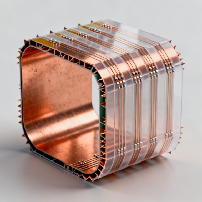
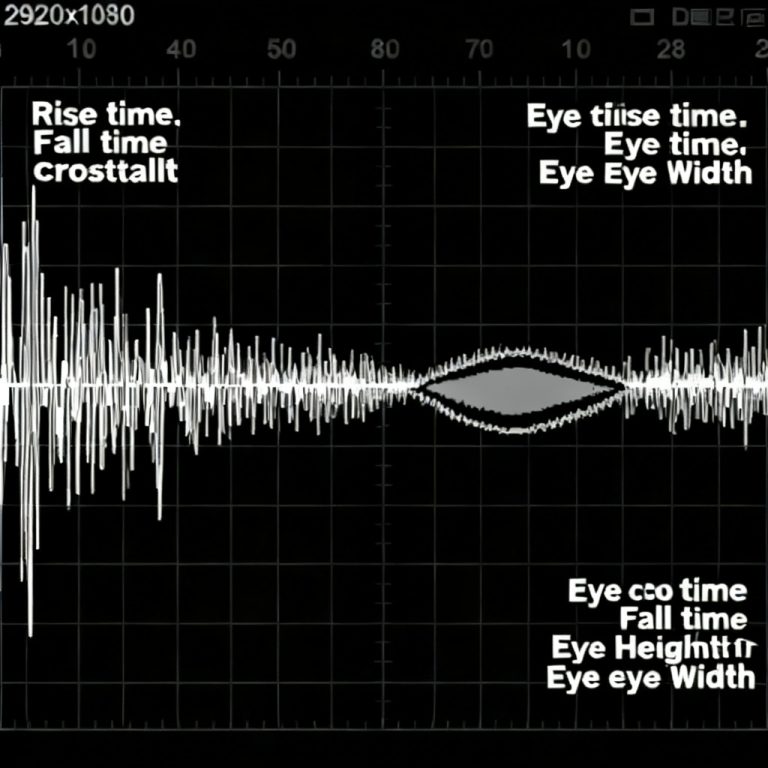
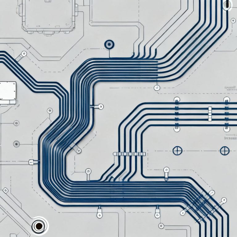
    This comprehensive Flexible Rigid Flex PCB Guide Materials Stackup Bend Cycles manual covers materials, stackup design, and bend cycles for engineers and buyers seeking reliable, high-performance interconnect solutions. Flexible and rigid-flex PCBs are essential for modern electronics, from wearables to aerospace. Core Topics: Substrates, adhesives, coverlays, copper foils, stiffeners, stackup rules, bend cycle testing, design…

    Read More Flexible Rigid Flex PCB Guide Materials Stackup Bend CyclesContinue

  • Flexible PCB Guide Single Double Multilayer Flex stackup diagram illustrating polyimide substrate layers, rolled annealed copper foil, and bend radius constraints
    Flexible PCB Guide

    Flexible PCB Guide Single Double Multilayer Flex

    Byroot 2026-05-232026-05-23

    Master the Flexible PCB Guide Single Double Multilayer Flex. Understand materials, design rules, stack-ups, manufacturing challenges, and applications. Your ultimate resource for B2B procurement for flexible PCB manufacturing and custom solutions. 1. What is a Flexible PCB? A flexible PCB (Flexible Printed Circuit Board) is a patterned arrangement of printed circuitry and components that utilizes…

    Read More Flexible PCB Guide Single Double Multilayer FlexContinue

  • Dielectric Loss and Dispersion in High Speed PCBs
    PCB Principles & Fundamentals | RF PCB Layout Guidelines

    Dielectric Loss and Dispersion in High Speed PCBs

    Byroot 2026-05-232026-05-23

    Dielectric Loss and Dispersion in High-Speed PCBs: The Ultimate Guide to Material Selection and Signal Integrity Dielectric Loss and Dispersion in High Speed PCBs are the dominant factors degrading signal integrity at multi-gigabit data rates. This guide synthesizes expert insights from leading engineering sources to help you master material selection, measurement, and mitigation strategies for…

    Read More Dielectric Loss and Dispersion in High Speed PCBsContinue

  • PCB Power Plane Resonance and Decoupling Network Design simulation graph plotting target impedance profiles, parallel anti-resonance peaks, and MLCC placement optimization
    PCB Principles & Fundamentals | Grounding Strategies

    PCB Grounding Strategies Single Point Multi Point and Mixed

    Byroot 2026-05-212026-05-21

    This comprehensive technical guide focuses on PCB Grounding Strategies Single Point Multi Point and Mixed design for hardware engineers. In printed circuit board layouts, selecting the correct grounding approach is the most critical factor for electromagnetic compatibility (EMC), signal integrity, and system reliability. This manual explores their principles, applications, advantages, and best practices. Core Concepts…

    Read More PCB Grounding Strategies Single Point Multi Point and MixedContinue

  • PCB Power Plane Resonance and Decoupling Network Design simulation graph plotting target impedance profiles, parallel anti-resonance peaks, and MLCC placement optimization
    PCB Principles & Fundamentals | Power Plane Resonance

    PCB Power Plane Resonance and Decoupling Network Design

    Byroot 2026-05-212026-05-21

    Master the critical relationship between PCB power plane resonance and decoupling network design. Learn how to mitigate impedance peaks, optimize capacitor selection, and ensure stable power delivery for high-speed digital and RF circuits. This comprehensive guide synthesizes expert knowledge for reliable PCB performance. PCB Power Plane Resonance and Decoupling Network Design Overview 1. Understanding PCB…

    Read More PCB Power Plane Resonance and Decoupling Network DesignContinue

  • PCB Crosstalk Causes Effects and Mitigation eye diagram analysis illustrating capacitive and inductive coupling noise between adjacent trace spacing on high-speed digital designs
    Crosstalk Mitigation | PCB Principles & Fundamentals

    PCB Crosstalk Causes Effects and Mitigation

    Byroot 2026-05-212026-05-22

    This comprehensive technical guide focuses on PCB Crosstalk Causes Effects and Mitigation for hardware engineers. PCB Crosstalk is the unwanted electromagnetic coupling between adjacent signal traces in a printed circuit board, directly impacting signal integrity. This manual explores its causes, effects, and proven mitigation strategies for high-speed digital and analog designs.   What Is PCB…

    Read More PCB Crosstalk Causes Effects and MitigationContinue

  • SPI in SMT Assembly Optimizing PCB
    Quality & Reliability

    SPI in SMT Assembly Optimizing PCB Quality

    Byroot 2026-05-212026-05-22

    Discover how SPI in SMT Assembly Optimizing PCB Quality transforms modern electronics manufacturing. In the fast-paced world of production, quality control is paramount. We understand that the key to producing high-quality PCBs lies in the details of our SMT assembly process. One crucial step that often goes unnoticed but plays a vital role in ensuring PCB quality is Solder Paste Inspection…

    Read More SPI in SMT Assembly Optimizing PCB QualityContinue

  • PCB Return Path and Via Inductance High Speed Rules simulation plot illustrating continuous ground reference plane transitions, parasitic via stubs, and signal integrity optimization
    PCB Principles & Fundamentals | Return Path & Via Inductance

    PCB Return Path and Via Inductance High Speed Rules

    Byroot 2026-05-212026-05-21

    This comprehensive guide covers essential PCB Return Path and Via Inductance High Speed Rules for hardware engineers. In modern design, ensuring a continuous PCB return path and minimizing via inductance are critical to achieving pristine signal integrity and passing strict EMI compliance testing. Understanding the PCB Return Path: Foundation of Signal Integrity The Principle of…

    Read More PCB Return Path and Via Inductance High Speed RulesContinue

  • Power Integrity in PCB Design PDN Decoupling Ripple simulation plot illustrating target impedance curves, multilayer power distribution network stackup, and MLCC capacitor placement.
    PCB Principles & Fundamentals | Power Integrity for PCBs

    Power Integrity in PCB Design PDN Decoupling Ripple

    Byroot 2026-05-202026-05-21

    This comprehensive technical manual focuses on Power Integrity in PCB Design PDN Decoupling Ripple analysis. Mastering Power Integrity in PCB Design is non-negotiable for modern high-speed, high-reliability applications. This guide provides an exhaustive, expert-level overview of Power Distribution Networks (PDNs), decoupling capacitor strategies, and ripple suppression, ensuring your board delivers clean, stable power to every…

    Read More Power Integrity in PCB Design PDN Decoupling RippleContinue

  • RF PCB Layout Guidelines diagram illustrating high-frequency component placement optimization with microstrip transmission lines, continuous ground plane via stitching, and impedance control
    PCB Principles & Fundamentals | RF PCB Layout Guidelines

    RF PCB Layout Guidelines

    Byroot 2026-05-202026-05-20

    Mastering RF PCB layout guidelines is essential for reliable high-frequency circuit performance. This pillar guide covers stack-up, grounding, via stitching, impedance control, and signal integrity for successful RF PCB design. 1. RF PCB Layout Guidelines for Stack-Up Design RF PCB layout guidelines for stack-up design require careful material selection and layer symmetry. The stack-up foundation…

    Read More RF PCB Layout GuidelinesContinue

Page navigation

Previous PagePrevious 1 2 3 4 5 6 Next PageNext

© 2026 PCB Types Powered by PCBTypes

  • Home