PCB Assembly (PCBA): SMT, Through‑Hole & Inspection – The Complete Guide
PCB Assembly PCBA SMT Through Hole Inspection is the ultimate framework for evaluating electronic manufacturing quality. PCB Assembly (PCBA) is the process of soldering electronic components onto a bare PCB to create a functional circuit. It is the critical step transforming design into working products.
What Is PCB Assembly (PCBA)? SMT, Through‑Hole & Inspection Explained
PCB Assembly (PCBA) encompasses the entire process of mounting components onto a printed circuit board. This comprehensive guide covers every aspect of PCBA, from component placement to quality assurance, based on the latest industry standards and best practices. The three core methods are SMT, THT, and mixed technology, each with unique advantages for different applications.

Surface Mount Technology (SMT) – The Industry Standard for PCB Assembly
SMT Definition and Key Advantages
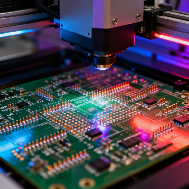
Surface Mount Technology (SMT) is the dominant assembly method where components are mounted directly onto the PCB surface. PCB Assembly using SMT has largely replaced through‑hole technology in high‑volume production due to efficiency and miniaturization capabilities. SMT components, such as resistors, capacitors, and ICs, have small leads or no leads at all, allowing for higher component density and smaller board sizes.
- High Component Density: SMT enables placement of hundreds of components on both sides of the PCB, maximizing functionality in compact designs.
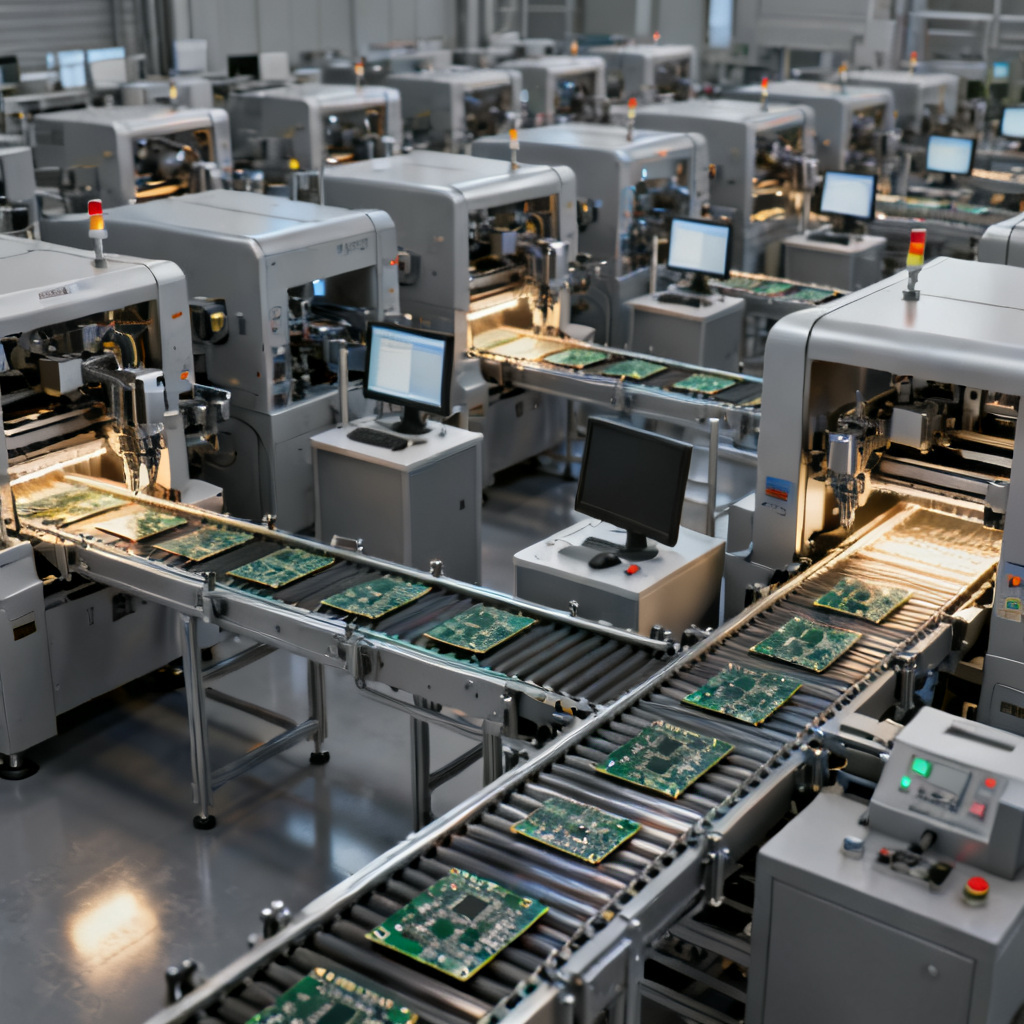
- Cost‑Effective for High Volume: Automated pick‑and‑place machines achieve high throughput, reducing labor costs.
- Improved Performance: Shorter signal paths reduce parasitic inductance and capacitance, enhancing high‑frequency performance.
- Better Mechanical Stability: SMT components are less prone to vibration‑induced failures compared to through‑hole parts.
The SMT Assembly Process Step‑by‑Step
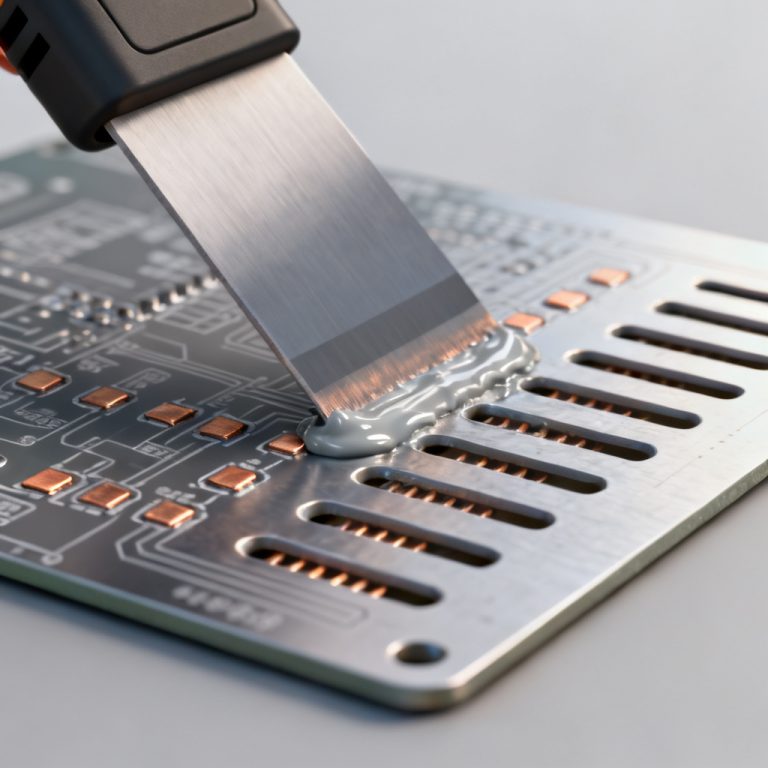
- Solder Paste Application: A stainless steel stencil applies solder paste (solder powder and flux) onto PCB pads. The stencil openings align precisely with pad locations.
- Pick‑and‑Place: High‑speed automated machines place components onto solder paste with precision, often using vision systems for alignment.
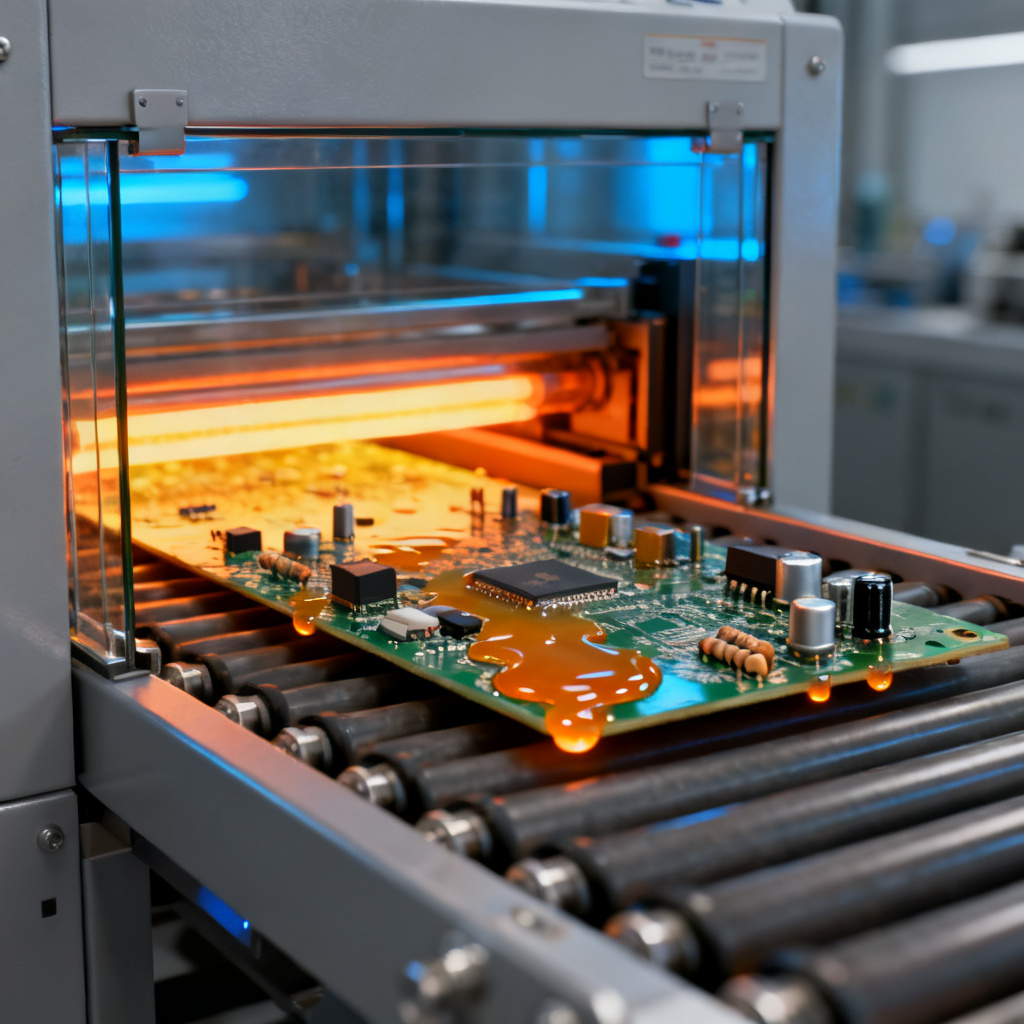
- Reflow Soldering: The board passes through a reflow oven with multiple temperature zones (preheat, soak, reflow, cooling). Solder paste melts, forming permanent electrical and mechanical connections.
- Inspection: Automated Optical Inspection (AOI) and X‑ray inspection verify solder joint quality and component placement.
SMT vs. Through‑Hole: When to Choose SMT
SMT is ideal for high‑density designs (e.g., smartphones, IoT devices), high‑volume production, and applications requiring high‑speed signal integrity. However, SMT is not suitable for high‑power or high‑voltage components, and it is less robust for heavy or large components.
Through‑Hole Technology (THT) – Strength and Reliability in PCB Assembly
THT Definition and Key Advantages
Through‑Hole Technology (THT) involves inserting component leads through pre‑drilled holes on the PCB and soldering them on the opposite side. PCB Assembly using THT remains essential for specific applications, especially in B2B and industrial sectors, due to superior mechanical strength and power handling.
- Superior Mechanical Strength: Components are physically anchored through the board, ideal for high‑stress environments (automotive, aerospace, military).
- Ease of Manual Assembly and Rework: THT components are easier to solder and replace by hand, beneficial for prototyping and low‑volume production.
- High Power Handling: Through‑hole components dissipate more heat, suitable for power supplies, relays, and connectors.
- Better Thermal and Electrical Conductivity: Larger leads and thicker copper traces improve performance in high‑current circuits.
The THT Assembly Process
- Component Insertion: Components are inserted into pre‑drilled holes manually or by automated insertion machines (axial, radial, or DIP inserters).
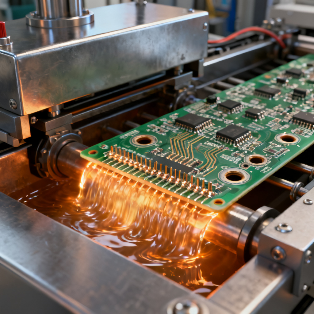
- Soldering: Two main methods: wave soldering (board passes over molten solder wave) or hand soldering (for prototypes or rework).
- Inspection: Visual inspection, AOI, and electrical testing ensure correct placement and solder quality.
THT vs. SMT: When to Choose THT
THT is preferred for high‑reliability applications (medical devices, military equipment), components requiring manual replacement (connectors, sockets), and high‑power or high‑voltage circuits. Drawbacks include lower component density, higher cost for high‑volume production, and limited high‑frequency performance.
Mixed Technology Assembly – The Best of Both Worlds in PCB Assembly
In modern B2B PCB Assembly, mixed technology (combining SMT and THT on the same board) is common. For example, a board may use SMT for most components to save space and cost, while using THT for connectors, power components, or heat sinks. The assembly process requires careful planning:
- Double‑sided SMT: Components placed on both sides, with bottom side often using smaller parts.
- Pin‑in‑Paste (PiP): Hybrid method where through‑hole components are placed on solder paste and reflowed with SMT parts, eliminating wave soldering.
- Selective Soldering: For mixed boards, wave soldering is used only for THT components, while SMT parts are protected by a mask or fixture.
Inspection and Quality Control – Ensuring Zero Defects in PCB Assembly
Automated Optical Inspection (AOI)
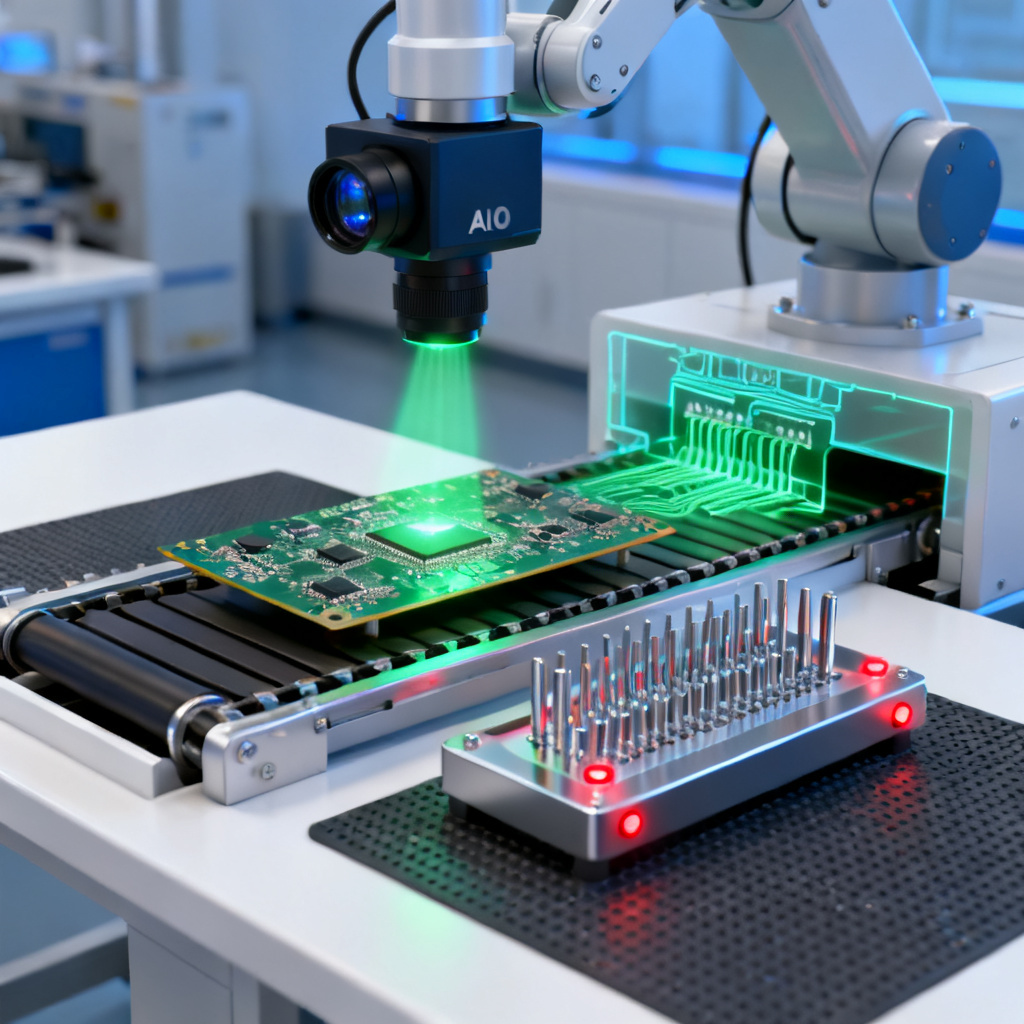
High‑resolution cameras capture PCB images and compare them to a CAD model. AOI detects missing components, incorrect polarity, solder bridges, tombstoning, and insufficient solder. It is fast, non‑contact, and suitable for high‑volume lines, but cannot inspect hidden solder joints (e.g., under BGA components).
X‑Ray Inspection
X‑rays penetrate the board to create a shadow image revealing internal solder joints. X‑ray detects voiding in BGA or QFN solder joints, hidden bridges, misalignment, and head‑in‑pillow defects. It is essential for dense SMT assemblies but has higher cost and slower speed.
In‑Circuit Testing (ICT)
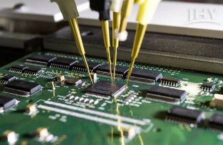
A bed‑of‑nails fixture contacts test points to measure resistance, capacitance, and diode behavior. ICT detects shorts, opens, incorrect component values, and missing parts. It offers high coverage and is fast for high‑volume production, but requires dedicated fixtures.
Functional Testing (FCT)
The assembled board is powered and tested under simulated operating conditions. FCT validates overall functionality, signal integrity, and performance under load. It ensures the board works as intended but may not catch subtle manufacturing defects.
Visual Inspection
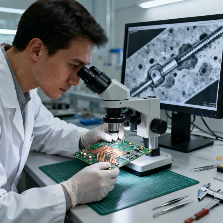
Operators inspect boards under magnification (microscopes or magnifying lenses). Visual inspection detects solder joint quality, component orientation, and cosmetic defects. It is low cost and flexible for prototypes but prone to human error.
Solder Joint Quality Standards (IPC‑A‑610)
The IPC‑A‑610 standard defines three classes: Class 1 (general electronics), Class 2 (dedicated service electronics), and Class 3 (high‑reliability electronics). For B2B customers, Class 2 or Class 3 is typically required. Key criteria include smooth, concave fillets with good wetting, component alignment within 25% of pad width for SMT, and no solder bridges or voids over 25% of joint area.
Defect Prevention and Best Practices for PCB Assembly
Design for Assembly (DFA)
- Pad Design: Follow IPC‑7351 standards for SMT pad sizes and tolerances.
- Component Spacing: Allow sufficient gap for pick‑and‑place nozzles and rework.
- Thermal Management: Avoid placing large THT components near heat‑sensitive SMT parts.
Solder Paste Selection
Use Type 3 or Type 4 solder paste for fine‑pitch SMT. For lead‑free assemblies, SAC305 (Sn‑Ag‑Cu) is the most common alloy.
Reflow Profile Optimization
Ensure the reflow profile matches solder paste specification (ramp rate, peak temperature, time above liquidus). Use nitrogen atmosphere for fine‑pitch or high‑reliability boards to reduce oxidation.
Wave Soldering for THT
Use flux compatible with the solder alloy and board surface finish. Maintain proper wave height and contact time (typically 2–4 seconds).
Advanced Topics – Fine‑Pitch, BGA, and Lead‑Free in PCB Assembly
Fine‑Pitch SMT
Components with lead pitches below 0.5 mm (QFP, QFN) require precise placement and inspection. Use high‑accuracy pick‑and‑place machines with vision alignment, AOI with high magnification and 3D capabilities, and X‑ray for hidden joints.
Ball Grid Array (BGA)
BGAs have solder balls underneath the package. Key considerations: stepped stencil to prevent solder bridging, slow ramp rate to avoid thermal shock, and mandatory X‑ray inspection for voids, bridges, and non‑wetting.
Lead‑Free Assembly
RoHS compliance requires lead‑free solders (SAC305). Challenges include higher reflow temperatures (260°C vs. 230°C), increased voiding and tin whiskers, and need for nitrogen atmosphere to improve wetting.
Cost Factors and Lead Times in B2B PCB Assembly
| Factor | Impact on Cost | Typical Lead Time |
|---|---|---|
| Component Sourcing | Custom or rare parts increase cost and lead time | 2–8 weeks |
| Board Complexity | More layers, fine‑pitch, or mixed technology add cost | 1–3 weeks |
| Volume | High volume reduces per‑unit cost | 2–4 weeks |
| Inspection Requirements | Full X‑ray or Class 3 inspection adds cost | 1–2 weeks |
| Testing | ICT or FCT requires fixture investment | 1–2 weeks |
Turnkey vs. Consignment: Turnkey (we source all components) is more convenient but may have higher material costs. Consignment (you provide components) reduces cost but requires inventory management.
Why Choose Our PCB Assembly Services?
As a trusted B2B partner, we offer full‑service PCBA from prototype to high‑volume production, including SMT, THT, mixed technology, and all inspection methods. Our advanced capabilities include fine‑pitch (down to 0.3 mm), BGA, QFN, and lead‑free assembly. We comply with IPC‑A‑610 Class 2 and Class 3 standards, using AOI, X‑ray, ICT, and FCT. Prototypes are available in 5–7 business days; production in 2–4 weeks. We source components from authorized distributors to avoid counterfeits.
Frequently Asked Questions About PCB Assembly (PCBA)
What is the difference between SMT and THT in PCB Assembly?
SMT (Surface Mount Technology) mounts components directly on the PCB surface, offering high density and cost efficiency for high volume. THT (Through‑Hole Technology) inserts leads through holes, providing superior mechanical strength for high‑reliability applications.
How does inspection ensure quality in PCB Assembly?
Inspection methods like AOI, X‑ray, ICT, and FCT detect defects such as solder bridges, voids, and incorrect placement. IPC‑A‑610 standards define acceptance criteria for Class 1, 2, and 3 assemblies, ensuring reliability.
What is mixed technology in PCB Assembly?
Mixed technology combines SMT and THT on the same board, optimizing space and cost for complex designs. It uses techniques like pin‑in‑paste and selective soldering to handle both component types.
Why choose your company for PCB Assembly services?
We provide comprehensive PCBA with advanced capabilities, fast turnaround, IPC‑A‑610 compliance, and global component sourcing. Our services cover SMT, THT, mixed technology, and full inspection to meet B2B requirements.
“`