PCB Assembly Defects Solder Bridging Tombstoning Voids
Master PCB assembly defects: solder bridging, tombstoning, and voids. Learn root causes, advanced prevention techniques, and reliable solutions from industry experts to boost yield and reliability.
1. Solder Bridging: Causes, Prevention, and Detection
Solder bridging occurs when molten solder creates an unintended electrical connection between two or more adjacent conductors, such as pads, pins, or traces. This typically results in a short circuit. Understanding solder bridging is critical for high-quality PCB assembly.

1.1 Root Causes of Solder Bridging
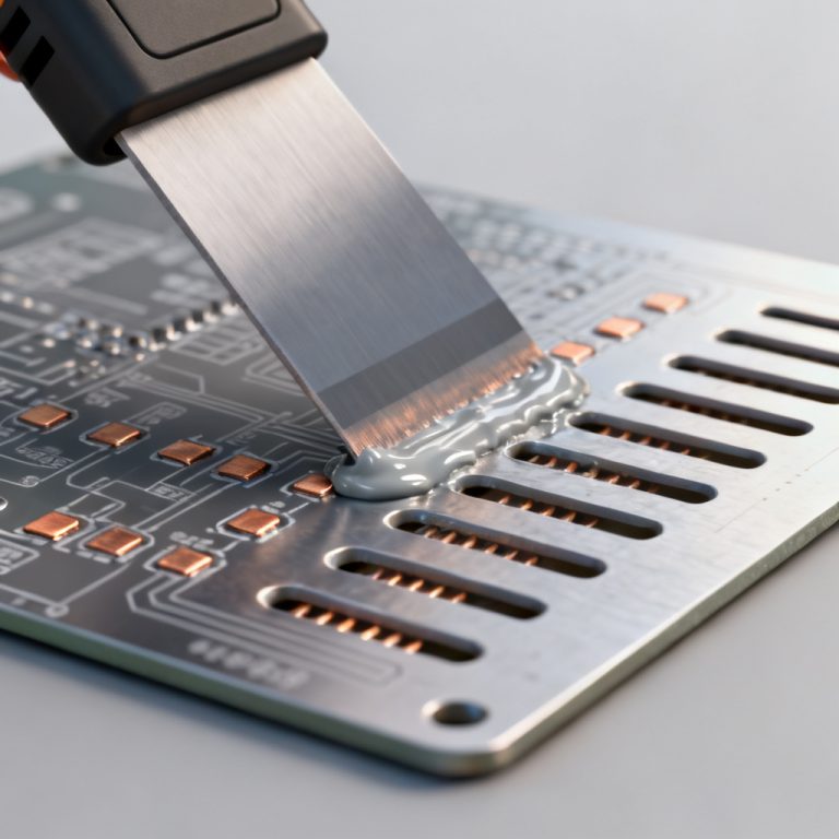
- Excessive Solder Paste Volume: Too much paste applied during stencil printing is the primary cause. This is often due to oversized stencil apertures or incorrect paste thickness.
- Poor Solder Paste Registration: Misalignment between the stencil and the PCB pads leads to paste deposition on non-wettable areas or between pads.
- Insufficient Solder Mask Webbing (Solder Mask Slivers): When the solder mask between fine-pitch pads is too narrow or missing, solder can easily bridge across.
- Inadequate Pad Spacing: Design rules that violate the PCB manufacturer’s capabilities (e.g., pad-to-pad gaps < 0.15mm for standard processes) increase bridging risk.
- Incorrect Reflow Profile: A ramp-to-peak profile that is too slow can cause paste to slump and flow into adjacent areas before solidification. Excessive peak temperature also promotes bridging.
- Component Placement Pressure: Excessive placement force can squeeze paste out from under the component, creating bridges.
- Warpage or Coplanarity Issues: PCB or component warpage during reflow can cause uneven contact, leading to solder flow into unintended gaps.
- Surface Contamination: Residues from fabrication (e.g., flux, oils) or handling can prevent proper solder wetting, causing bridges.
1.2 Prevention Strategies for Solder Bridging
- Optimize Stencil Design: Reduce aperture area ratio for fine-pitch components (e.g., use a 1:1 ratio or slightly smaller for 0.4mm pitch QFPs). Use step stencils to reduce paste volume on dense areas while maintaining volume on larger components. Employ aperture shaping (e.g., home-plate or trapezoidal shapes) to control paste release.
- Enhance Solder Paste Properties: Use no-clean or water-soluble pastes with high tack and anti-slump characteristics. Control paste viscosity (typically 800-1200 kcps) and ensure proper mixing.
- Improve Solder Mask Quality: Specify a minimum solder mask sliver width of 0.1mm (4 mils) between pads. Use LPI (Liquid Photoimageable) solder mask for better resolution.
- Refine Reflow Profile: Implement a linear or “soak” profile with a controlled preheat slope (1-3°C/sec) to allow solvent evaporation and reduce slump. Keep peak temperature within 20-40°C above solder liquidus (e.g., 230-250°C for SAC305).
- Control Placement Accuracy: Maintain pick-and-place machine alignment within ±0.05mm for fine-pitch components. Use vision systems for centering.
- Design for Manufacturing (DFM): Increase pad-to-pad spacing where possible (minimum 0.2mm for standard SMT). Avoid 90-degree pad corners; use rounded or chamfered pads to reduce solder wicking. Incorporate solder thief pads (dummy pads) at the ends of fine-pitch rows.
1.3 Detection and Repair of Solder Bridging
- Visual Inspection: Use a microscope (10x-40x magnification) for manual inspection.
- Automated Optical Inspection (AOI): High-speed AOI systems can detect bridges by comparing solder joint shapes to golden boards.
- X-ray Inspection: Essential for hidden bridges under BGAs, QFNs, or components with bottom terminations. X-ray reveals the actual solder connection geometry.
- Repair: Remove bridges using a fine-tipped soldering iron with a desoldering braid (solder wick). For dense areas, use a hot air rework station with flux to reflow and remove excess solder. After repair, re-inspect with AOI or X-ray.
2. Tombstoning: Causes, Prevention, and Solutions
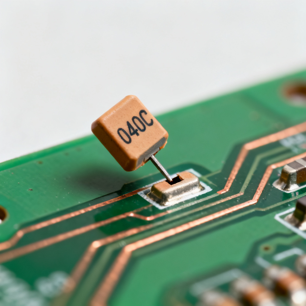
Tombstoning (also called “drawbridging” or “Manhattan effect”) is a defect where a surface-mount component, typically a small chip (e.g., 0402, 0603, 0805 resistor or capacitor), lifts vertically on one end while the other end remains soldered to the pad. This creates an open circuit. Preventing tombstoning is essential for reliable SMT assembly.
2.1 Root Causes of Tombstoning
- Uneven Wetting Forces: The primary cause is a mismatch in the surface tension forces acting on the two ends of the component during reflow. If one pad wets faster or with greater force than the other, the component tilts.
- Asymmetric Pad Design: Pads of unequal size (one significantly larger than the other) create unbalanced wetting forces. The larger pad pulls the component up.
- Thermal Imbalance: Uneven heating across the component. For example, if one pad is connected to a large ground plane (heat sink), it heats slower than the other pad, causing delayed wetting.
- Component Misplacement: A component placed off-center (even by 0.1mm) creates a lever effect, making one end more susceptible to lifting.
- Solder Paste Volume Imbalance: Unequal paste volume on the two pads (e.g., due to stencil aperture variation or paste slump) leads to different wetting forces.
- Incorrect Reflow Profile: A rapid ramp-up rate (>3°C/sec) can cause one end to reach reflow temperature before the other, accelerating tombstoning. Also, a slow cooling rate can exacerbate the effect.
- Component Weight and Size: Smaller, lighter components (e.g., 0402 and below) are more prone to tombstoning because their mass is insufficient to counteract the wetting forces.
- Solder Mask on Pad: If solder mask encroaches onto one pad, the effective pad area is reduced, altering wetting dynamics.
- Nitrogen Atmosphere: Using nitrogen in reflow can increase surface tension of molten solder, potentially worsening tombstoning if not carefully controlled.
2.2 Prevention Strategies for Tombstoning
- Optimize PCB Pad Design: Ensure both pads for a given component are identical in size, shape, and spacing. Follow IPC-7351B guidelines for land patterns. For small chip components, use “non-solder mask defined” (NSMD) pads to allow maximum pad area. Consider using “teardrop” or “fillet” pads to anchor the component ends.
- Control Solder Paste Application: Use a stencil with equal aperture sizes for both pads of a component. Maintain consistent paste height (typically 0.1-0.15mm for fine-pitch). Avoid paste slumping by using high-tack paste.
- Balance Thermal Mass: Add thermal relief spokes to pads connected to large copper pours (e.g., ground planes). Use “thermal vias” under pads to distribute heat evenly. Design the board layout to ensure symmetrical thermal paths for each component end.
- Refine Reflow Profile: Use a linear ramp rate of 1-2°C/sec to allow even heating. Implement a soak zone (150-180°C for 60-90 seconds) to equalize temperature across the board and components. Avoid excessive peak temperature; keep within 20-30°C above liquidus.
- Component Placement Optimization: Center components accurately using vision alignment. For very small components (0201, 01005), consider using “adhesive fixing” (dot of epoxy under the component) before reflow.
- Use Anti-Tombstoning Component Designs: Some component manufacturers offer “bottom-only termination” or “under-termination” designs that reduce lifting risk.
- Nitrogen Control: If using nitrogen, maintain oxygen levels below 50 ppm to reduce surface tension, but monitor for other effects.
2.3 Detection and Repair of Tombstoning
- Visual Inspection: Tombstoning is often visible to the naked eye or under low magnification (5-10x). Look for components standing upright.
- AOI: AOI systems can detect tombstoning by measuring component height or tilt angle.
- X-ray: For hidden components (e.g., under shields), X-ray can reveal tilted leads.
- Repair: Use a hot air rework station to reflow the lifted end. Apply flux to the lifted pad, then gently press the component down with tweezers while heating until the solder reflows. For severe cases, remove the component, clean pads, apply fresh solder paste, and reattach.
3. Voids: Causes, Prevention, and Detection
Voids are cavities or gas pockets trapped within a solder joint. They are most critical in BGA, QFN, and other area-array components where the joint is hidden and structural integrity is paramount. Managing voids is key for high-reliability PCB assembly.

3.1 Root Causes of Voids
- Outgassing from Solder Paste: Volatile solvents and flux components that do not fully evaporate during preheat get trapped as the solder solidifies. This is the most common cause.
- Insufficient Preheating: A too-short or too-low preheat zone fails to drive off solvents and moisture from the paste, PCB, and component surfaces.
- Moisture Absorption: PCBs (especially those with high Tg or organic substrates) and components (e.g., BGAs) can absorb moisture from the environment. During reflow, this moisture vaporizes, creating voids.
- Oxide or Contamination: Oxidized pad surfaces or component terminations prevent proper wetting, causing gas entrapment. Flux residues can also decompose.
- Solder Paste Chemistry: Some flux formulations (e.g., no-clean) are more prone to voiding than water-soluble types due to their higher solids content.
- Stencil Design Issues: Aperture shape and aspect ratio affect paste deposition. Thick stencils with small apertures can trap air.
- Reflow Profile: A fast ramp rate can cause rapid outgassing that exceeds the solder’s ability to release gas. A slow cooling rate allows more time for voids to form.
- Component Geometry: BGAs with large solder balls or small stand-off heights (e.g., 0.3mm) have less space for gas to escape.
3.2 Prevention Strategies for Voids
- Optimize Reflow Profile: Extend the preheat zone (150-180°C) to 90-120 seconds to ensure complete outgassing. Use a slow ramp rate (1-2°C/sec) in the preheat stage. Increase peak temperature by 5-10°C above the standard for the solder alloy to reduce solder viscosity, allowing bubbles to escape. Implement a “soak” profile with a plateau at 180-200°C for 60-90 seconds before ramp to peak.
- Control Material Quality: Use solder paste with low voiding formulations (e.g., “low void” or “vacuum reflow” compatible pastes). Look for IPC J-STD-005A classification. Ensure PCBs are baked before assembly if stored in high humidity (e.g., 125°C for 4 hours). Store components in dry cabinets (<30% RH) and bake moisture-sensitive devices per IPC/JEDEC J-STD-033.
- Improve Stencil Design: Use square or rectangular apertures with rounded corners for better paste release. For BGAs, consider using “via-in-pad” filled with conductive epoxy to reduce pad volume. Reduce stencil thickness for fine-pitch BGAs (e.g., 0.1mm for 0.4mm pitch).
- Vacuum Reflow (Void Reduction): Implement vacuum reflow technology. After the solder melts, a vacuum is applied (typically 10-50 mbar) to extract gases before solidification. This can reduce voiding to <5% for BGAs.
- Nitrogen Atmosphere: Using nitrogen in the reflow oven (oxygen < 50 ppm) reduces oxide formation and improves wetting, which helps release trapped gases.
- Design for Manufacturing (DFM): Avoid placing large ground planes directly under BGA pads without thermal relief. Use solder mask defined (SMD) pads for BGAs to reduce pad area and voiding risk. Ensure adequate clearance between pads for gas escape.
3.3 Detection and Acceptance Criteria for Voids
- X-ray Inspection: The primary method. 2D X-ray can show void area percentage. 3D X-ray (CT) provides volumetric data.
- Acceptance Criteria (per IPC-A-610G, Class 2 & 3): For BGA and QFN: Voids should not exceed 25% of the solder joint area (Class 2) or 15% (Class 3) when viewed in 2D X-ray. For through-hole components: Voids should not exceed 25% of the fillet area. For surface-mount components: Voids are generally acceptable if they do not compromise mechanical strength or electrical conductivity. IPC-7095C provides detailed guidance for BGAs.
- Cross-sectioning: Destructive analysis to confirm void size and location.
- Repair: For unacceptable voids (e.g., >25% in a critical BGA joint), remove the component, clean pads, apply fresh paste, and reflow with a optimized profile (consider vacuum reflow). For minor voids, reflow with flux may help.
Comparison: Solder Bridging vs. Tombstoning vs. Voids
| Defect Type | Primary Cause | Key Prevention | Detection Method |
|---|---|---|---|
| Solder Bridging | Excessive paste, poor registration | Stencil optimization, DFM | AOI, X-ray |
| Tombstoning | Uneven wetting, thermal imbalance | Pad symmetry, reflow profile | Visual, AOI |
| Voids | Outgassing, moisture | Preheat, vacuum reflow | X-ray |
Glossary: Industry Terminology
- Solder Bridging: Unintended solder connection between conductors causing short circuits.
- Tombstoning: Component lifting on one end due to unbalanced wetting forces.
- Voids: Gas pockets trapped in solder joints, affecting reliability.
- Reflow Profile: Temperature curve during soldering process.
- DFM (Design for Manufacturing): Design practices to improve manufacturability.
- AOI (Automated Optical Inspection): Machine vision for defect detection.
- BGA (Ball Grid Array): Surface-mount packaging with solder balls.
FAQ: Assembly Defects – Solder Bridging, Tombstoning, Voids
What is the most common cause of solder bridging?
Excessive solder paste volume is the most common cause of solder bridging, often due to oversized stencil apertures or incorrect paste thickness.
How can I prevent tombstoning in PCB assembly?
Prevent tombstoning by ensuring symmetric pad design, using balanced reflow profiles with slow ramp rates, and optimizing component placement accuracy.
What is the acceptable void percentage for BGA solder joints?
Per IPC-A-610G, voids should not exceed 25% of the solder joint area for Class 2 and 15% for Class 3 when viewed in 2D X-ray.
How does reflow profile affect assembly defects?
Incorrect reflow profiles can cause solder bridging, tombstoning, and voids. A slow ramp rate and proper soak zone help reduce these defects.
What is the difference between AOI and X-ray for defect detection?
AOI is effective for visible defects like bridging and tombstoning, while X-ray is essential for hidden defects like voids under BGAs.
Conclusion: A Holistic Approach to Defect Prevention
Solder bridging, tombstoning, and voids are interconnected challenges in PCB assembly. A single root cause—such as an incorrect reflow profile—can trigger all three. The most effective strategy is a holistic approach that integrates:
- DFM (Design for Manufacturing): Collaborate with your PCB manufacturer early to optimize pad geometry, thermal management, and solder mask.
- Process Control: Standardize stencil design, paste application, placement accuracy, and reflow profiles. Use SPC (Statistical Process Control) to monitor key parameters.
- Material Selection: Choose high-quality solder paste, PCBs, and components with low moisture sensitivity.
- Advanced Inspection: Implement AOI, X-ray, and in-line process monitoring to catch defects early.
- Continuous Improvement: Analyze defect data to identify trends and implement corrective actions.
By mastering these three common defects, you can significantly improve first-pass yield, reduce rework costs, and deliver reliable electronic products to your customers. For additional guidance, refer to industry standards like IPC-A-610 (Acceptability of Electronic Assemblies) and IPC-7095 (BGA Design and Assembly).