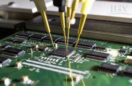
SMT Assembly Solder Paste Pick and Place Reflow
SMT assembly is the backbone of modern electronics manufacturing, enabling the production of compact, high‑performance printed circuit boards (PCBs). Unlike through‑hole technology, SMT assembly involves mounting components directly onto the surface of a PCB, which allows for higher component density, faster assembly, and improved electrical performance. The SMT assembly process consists of three critical stages: solder paste application, pick‑and‑place, and reflow soldering. Each stage requires precise control of materials, equipment, and environmental conditions to ensure reliable solder joints and high yield rates. This pillar content provides an in‑depth exploration of these processes, covering best practices, common challenges, and advanced techniques, based on insights from industry‑leading resources.
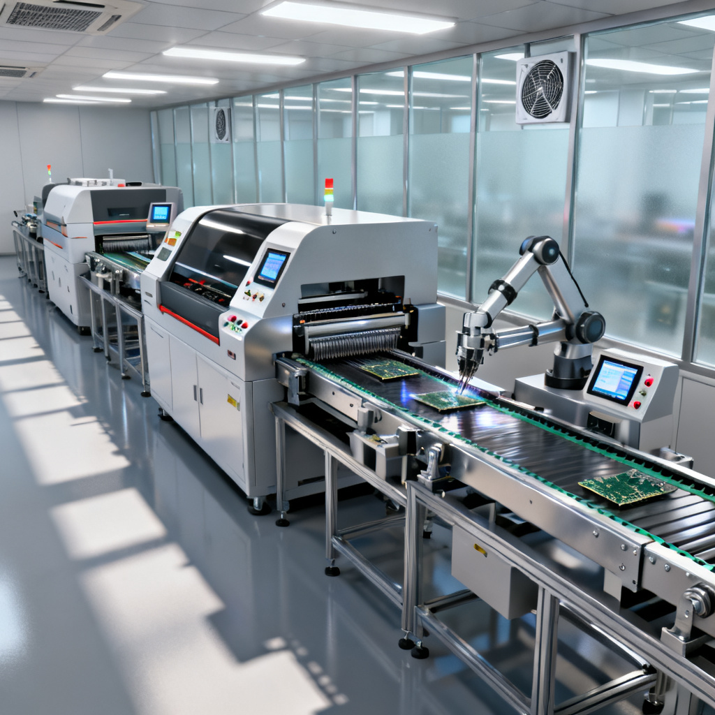
1. Solder Paste Application: The Foundation of SMT Assembly
1.1 What is Solder Paste?
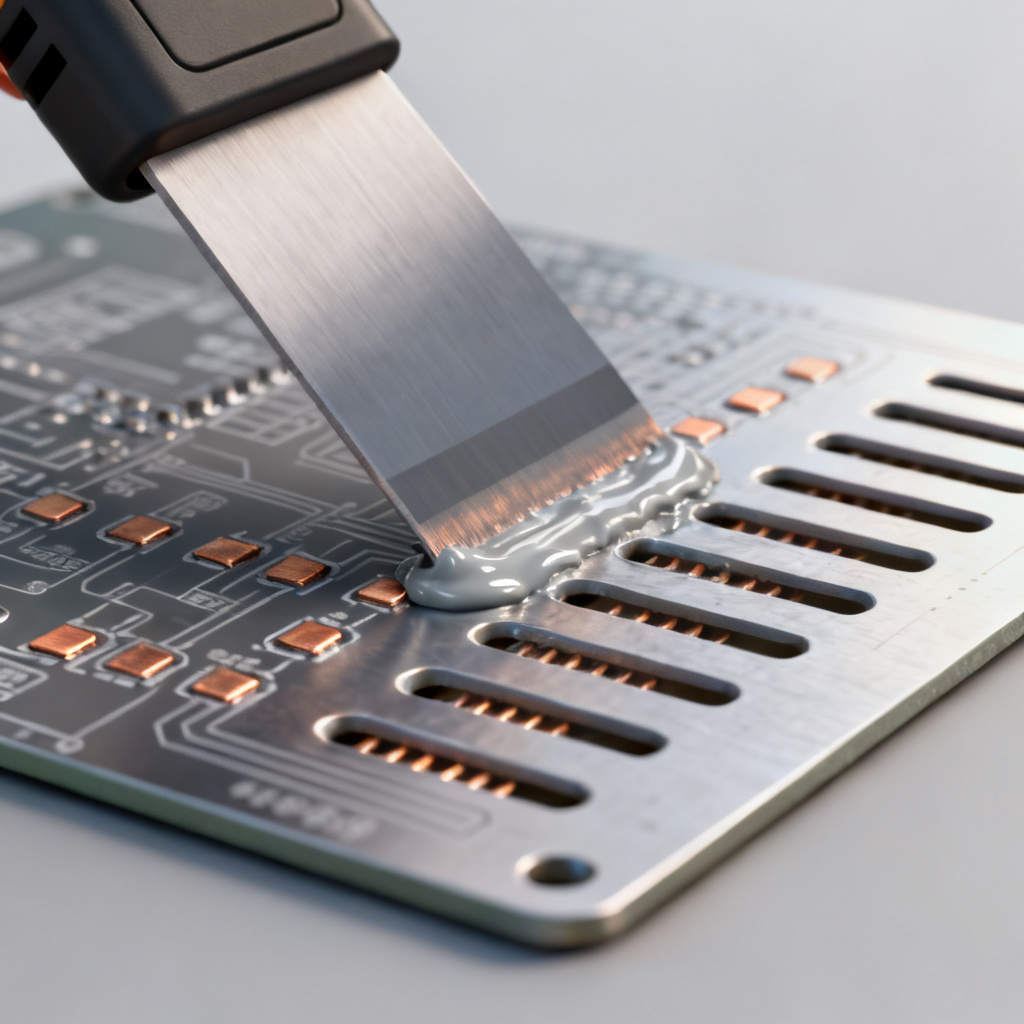
SMT assembly begins with solder paste, a mixture of solder alloy powder and flux. The flux serves multiple purposes: it removes oxides from the metal surfaces, promotes wetting, and prevents re‑oxidation during soldering. The solder powder is typically made from tin‑lead (SnPb) or lead‑free alloys (e.g., SAC305 – Sn96.5Ag3.0Cu0.5). The particle size is classified by type (e.g., Type 3, Type 4, Type 5), with finer particles used for fine‑pitch components. The viscosity and rheology of the paste are crucial for consistent printing.
1.2 Solder Paste Printing Process
The most common method for applying solder paste is stencil printing. A stainless steel or nickel stencil is aligned over the PCB, and a squeegee blade forces the paste through apertures onto the board’s pads. Key parameters include:
| Parameter | Typical Value | Impact on SMT Assembly |
|---|---|---|
| Squeegee pressure | 50–100 N | Excess pressure causes paste bleed; too little leads to insufficient deposit. |
| Squeegee speed | 20–50 mm/s | Affects paste volume consistency. |
| Squeegee angle | 60° | Standard angle for optimal paste rolling. |
| Stencil thickness | 0.1–0.2 mm | Thicker stencils deposit more paste for large components. |
| Aperture area ratio | >0.66 | Ensures good paste release from stencil. |
| Separation speed | 1–5 mm/s | Slow separation reduces paste bridging and smearing. |
| Temperature | 20–25°C | Prevents paste drying or absorption. |
| Humidity | 30–60% RH | Controls paste rheology. |
1.3 Solder Paste Inspection (SPI)
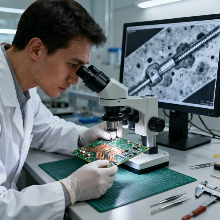
After printing, solder paste inspection (SPI) systems use 3D laser or structured light to measure paste volume, height, area, and alignment. SPI is critical because over 60% of SMT assembly defects originate from paste application issues. Common defects include:
- Insufficient solder: Leads to open joints.
- Excess solder: Causes bridging or solder balls.
- Smear or bridging: Often due to high squeegee pressure or poor stencil alignment.
SPI data is fed back to the printer for real‑time adjustments (closed‑loop control).
1.4 Advanced Techniques
- Step stencils: Used for boards with mixed component sizes (e.g., large QFNs and tiny 0201s). Different thicknesses in specific areas optimize paste volume.
- Electroformed stencils: Provide better aperture geometry and release for fine‑pitch applications.
- Paste jetting: A non‑contact method (e.g., from MyData or Asymtek) that deposits paste droplets directly onto pads, ideal for prototypes or high‑mix low‑volume production.
2. Pick‑and‑Place: Precision Component Mounting
2.1 Overview of Pick‑and‑Place Equipment
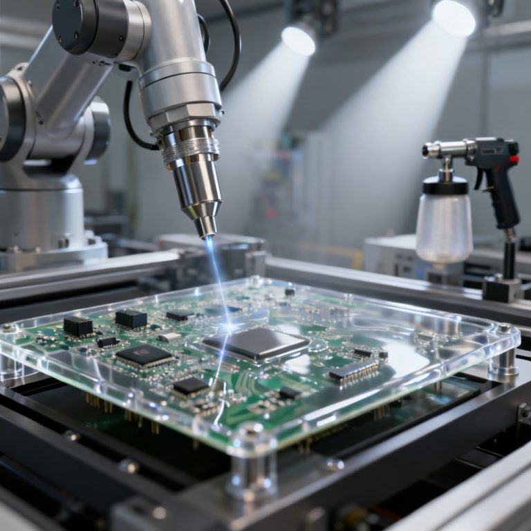
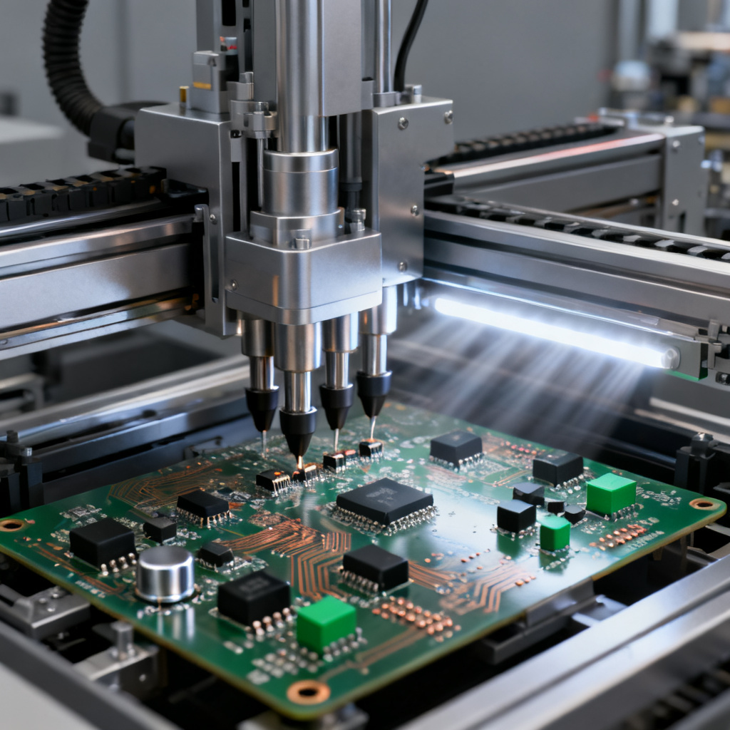
Pick‑and‑place machines are robotic systems that retrieve components from feeders (tape, tray, or tube) and place them onto the PCB with high speed and accuracy. Most modern machines use vision systems to align components to pads. Key specifications include:
| Specification | Typical Value | Relevance to SMT Assembly |
|---|---|---|
| Placement speed | 50,000–100,000 CPH (high‑speed) | Determines throughput for mass production. |
| Placement accuracy | ±50 μm (standard), ±30 μm (fine‑pitch) | Critical for pick‑and‑place of small components. |
| Feeder capacity | Depends on machine model | Determines the number of unique component types. |
2.2 The Placement Process
The process involves four steps:
- Component pickup: A vacuum nozzle picks the component from the feeder. Nozzle size and shape must match the component surface (e.g., flat, concave, or soft‑touch for delicate parts).
- Vision alignment: The component is imaged by a camera (downward‑looking for leads or upward‑looking for body). The system calculates the component’s centroid and rotation, then adjusts the placement position.
- Placement: The nozzle descends to the PCB and releases the component with controlled force (typically 0.5–5 N). Excessive force can damage the component or cause solder paste displacement.
- Inspection: Some machines include on‑the‑fly inspection to verify component presence and orientation.
2.3 Component Handling Challenges
- Small components (e.g., 0201, 01005): Require precise nozzle alignment and anti‑static measures to prevent “tombstoning” (one end lifts during reflow soldering).
- Large components (e.g., BGAs, QFNs): Need accurate paste deposition and placement to avoid solder ball bridging or opens. Vacuum hold‑down is critical for warped boards.
- Odd‑form components (e.g., connectors, shields): Often require specialized nozzles or tray feeders.
2.4 Advanced Pick‑and‑Place Technologies
- Dual‑beam or multi‑head systems: Increase throughput by placing multiple components simultaneously.
- 3D vision and laser alignment: For components with non‑planar surfaces (e.g., connectors with stand‑offs).
- Automatic nozzle changer: Allows rapid switching between nozzle types for different component sizes.
2.5 Quality Control: Post‑Placement Inspection
After placement, an automated optical inspection (AOI) system checks for missing, misaligned, or rotated components. AOI uses image comparison against a golden board. Some systems also measure component height to detect “pop‑corning” (component cracking due to moisture). If defects are found, the board is either reworked or scrapped.
3. Reflow Soldering: Creating Reliable Solder Joints
3.1 The Reflow Process
Reflow soldering is the final SMT assembly step, where the solder paste is melted to form permanent electrical and mechanical connections. The process is performed in a convection reflow oven (with or without nitrogen atmosphere). The oven has multiple heating zones, each set to a specific temperature. The PCB travels through these zones on a conveyor belt.
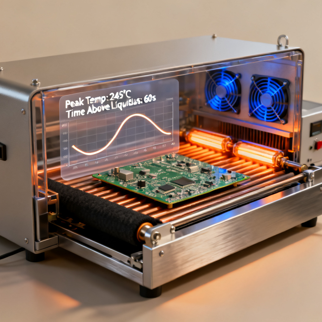
The standard reflow profile consists of four stages:
- Preheat (soak zone): The board is gradually heated from room temperature to about 150–170°C at a rate of 1–3°C/s. This activates the flux, removes solvents, and reduces thermal shock.
- Thermal soak: The board is held at 150–170°C for 60–120 seconds. This allows the flux to clean the surfaces and ensures uniform temperature across the board.
- Reflow (peak zone): The temperature rises rapidly to the peak temperature (typically 30–40°C above the melting point of the solder alloy). For lead‑free SAC305, the peak is 235–245°C, with a time above liquidus (TAL) of 30–90 seconds. The solder melts, wets the pads, and forms the joint.
- Cooling: The board is cooled at a rate of 2–4°C/s to solidify the solder joints. Fast cooling produces a finer grain structure, which improves joint strength.
3.2 Reflow Profile Optimization
A properly optimized profile is critical to avoid defects. Key parameters include:
- Ramp‑to‑soak slope: Too steep can cause solder balls or component cracking; too slow can cause excessive oxidation.
- Soak time: Insufficient soak leads to cold joints; excessive soak burns off flux, causing reoxidation.
- Peak temperature and TAL: Too low results in incomplete wetting; too high damages components or causes pad lifting.
- Cooling rate: Slow cooling leads to large grain size and weak joints; rapid cooling can cause thermal stress and cracks.
3.3 Common Reflow Defects and Solutions
| Defect | Root Cause | Solution |
|---|---|---|
| Solder bridging | Excess solder or insufficient pad spacing | Reduce paste volume, increase pad gap, or use solder mask between pads. |
| Tombstoning | Uneven wetting forces | Balance pad sizes, ensure uniform paste deposition, use slower heating in soak zone. |
| Voiding | Gas bubbles trapped in solder joint | Use low‑void flux, increase soak time, or apply vacuum reflow. |
| Head‑in‑pillow (HIP) | Solder ball and paste do not coalesce | Ensure proper paste volume, use nitrogen atmosphere, optimize profile. |
| Solder balling | Paste oxidation or high humidity | Reduce paste oxidation, control humidity, adjust squeegee pressure. |
3.4 Advanced Reflow Technologies
- Nitrogen reflow: Using nitrogen (N₂) in the oven reduces oxidation, improves wetting, and reduces voiding. It is essential for lead‑free soldering of fine‑pitch components.
- Vapor phase reflow: Uses a vapor blanket (e.g., perfluoropolyether) to heat the board uniformly. This eliminates temperature gradients and is ideal for complex boards with high thermal mass.
- Vacuum reflow: A vacuum is applied during the reflow stage to remove voids, especially for high‑reliability applications (e.g., automotive, aerospace).
- Convection‑dominated vs. infrared (IR) ovens: Modern ovens use forced convection for better heat transfer and uniformity, while IR is used for selective heating.
3.5 Quality Control: Post‑Reflow Inspection
After reflow soldering, boards undergo:
- Automated X‑ray inspection (AXI): Detects hidden defects such as voids, solder bridges under BGAs, and insufficient solder in through‑hole components (if used in mixed technology).
- AOI again: Confirms component presence, polarity, and solder joint appearance (e.g., fillet shape, wetting angle).
- Electrical testing: In‑circuit test (ICT) or flying probe test checks for shorts, opens, and component values.
4. Integration and Best Practices for SMT Assembly
4.1 Process Flow Optimization
To achieve high yield and throughput, the three stages must be tightly integrated:
- Stencil design must match component pitch and pad geometry.
- Pick‑and‑place programming should account for component weight, size, and sensitivity to heat.
- Reflow profile must consider the thermal mass of the board and components (e.g., large copper planes, BGAs).
- Data feedback loops: SPI data informs stencil adjustments; AOI data informs placement optimization; X‑ray data informs reflow profile tuning.
4.2 Material Selection
- Solder paste: Choose alloy based on end‑use (lead‑free for RoHS compliance, SnPb for legacy or high‑reliability). Flux type (RMA, no‑clean, water‑wash) depends on post‑solder cleaning requirements.
- Stencil material: Stainless steel for durability, nickel for fine‑pitch, and electroformed for best release.
- Flux: For no‑clean processes, ensure flux residue is non‑conductive (SIR test). For water‑wash, use water‑soluble flux.
4.3 Environmental and Safety Considerations
- Lead‑free soldering requires higher temperatures, which can degrade PCB materials (e.g., FR‑4) and components. Use high‑Tg laminates.
- Nitrogen atmosphere reduces oxidation but adds cost. Evaluate ROI for high‑reliability products.
- Fume extraction is mandatory for solder paste and reflow processes to protect operators from flux fumes.
4.4 Troubleshooting Common Issues
| Issue | Root Cause | Solution |
|---|---|---|
| Insufficient solder | Stencil aperture clogged | Clean stencil; increase squeegee pressure. |
| Component shift | Vibration during reflow | Reduce conveyor speed; use slower cooling. |
| Solder balling | Paste oxidation | Use fresh paste; control humidity. |
| Voiding | Flux outgassing | Increase soak time; use vacuum reflow. |
| Cold joints | Low peak temperature | Increase peak temperature; extend TAL. |
4.5 Comparison: Our SMT Assembly Services vs. Industry Standards
Our SMT assembly services offer advanced capabilities including 100% X‑ray inspection, nitrogen reflow for fine‑pitch components, and closed‑loop SPI feedback. We maintain defect rates below 50 ppm, exceeding the industry average of 100–200 ppm for standard pick‑and‑place and reflow soldering processes. Our process engineers optimize every profile based on board thermal mass, ensuring consistent results for both prototype and high‑volume runs.
5. FAQ: SMT Assembly
What is SMT assembly?
SMT assembly stands for Surface Mount Technology assembly, a process where electronic components are mounted directly onto the surface of a printed circuit board (PCB) using solder paste, pick‑and‑place machines, and reflow soldering.
What are the three main steps of SMT assembly?
The three main steps of SMT assembly are: applying solder paste to the PCB pads, placing components using pick‑and‑place equipment, and melting the paste in a reflow soldering oven to form permanent connections.
How do I choose the right solder paste for SMT assembly?
Choosing the right solder paste for SMT assembly depends on the alloy (lead‑free for RoHS, SnPb for high‑reliability), particle size (Type 3–5 for fine‑pitch), and flux type (no‑clean, water‑wash, or RMA).
What causes tombstoning in SMT assembly?
Tombstoning in SMT assembly occurs when one end of a component lifts during reflow soldering due to uneven wetting forces. It can be minimized by balancing pad sizes, ensuring uniform solder paste deposition, and optimizing the reflow profile.
How can I reduce voiding in reflow soldering?
Voiding in reflow soldering can be reduced by using low‑void flux, extending the soak time in the reflow profile, or applying vacuum reflow soldering for high‑reliability applications.
What is the difference between AOI and AXI in SMT assembly?
AOI (Automated Optical Inspection) checks component presence, alignment, and solder joint appearance after pick‑and‑place and reflow soldering, while AXI (Automated X‑ray Inspection) detects hidden defects like voids and solder bridges under components like BGAs in SMT assembly.