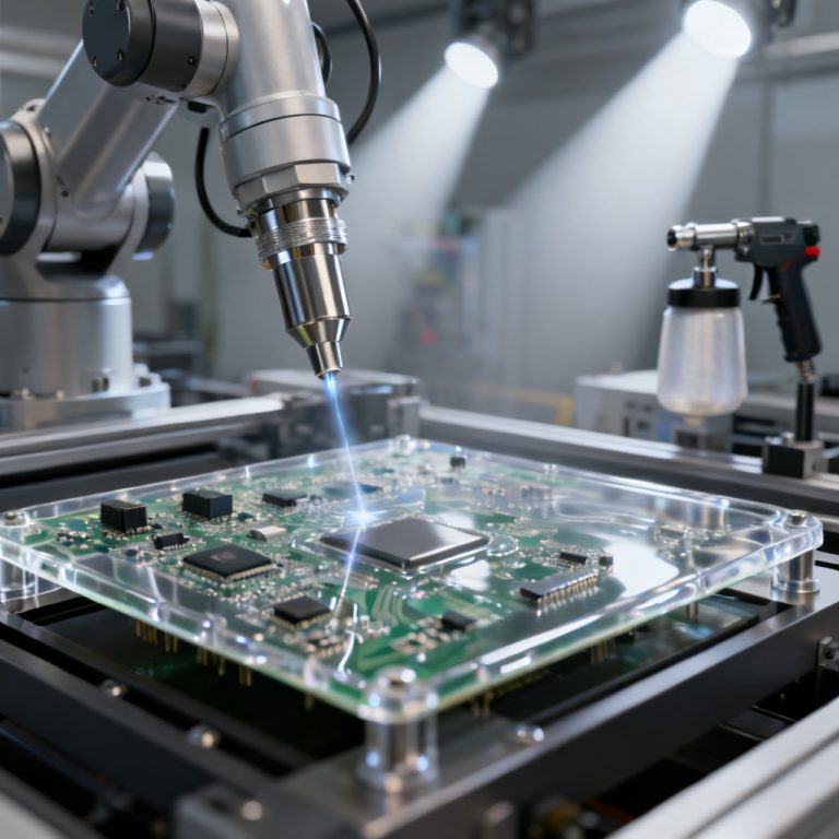
PCB Assembly PCBA Guide SMT Through Hole AOI
This PCB Assembly PCBA Guide covers SMT, through‑hole technology, and AOI inspection in full depth. It is the definitive resource for B2B buyers seeking reliable, high‑yield assembly for their electronic products.
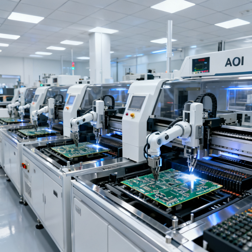
Surface Mount Technology (SMT) – The Modern Standard in PCB Assembly
PCB assembly using SMT mounts components directly onto the board surface. This method enables high‑density, high‑speed, and fully automated production.
1.1 The SMT Process: Step‑by‑Step
The SMT process in PCB assembly follows a precise automated sequence. Each step is critical for final quality.
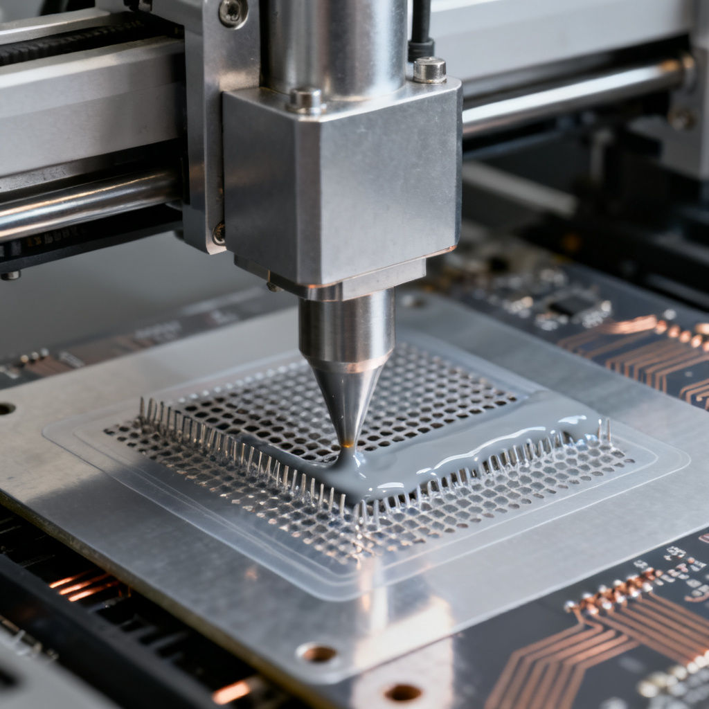
Step 1: Solder Paste Printing
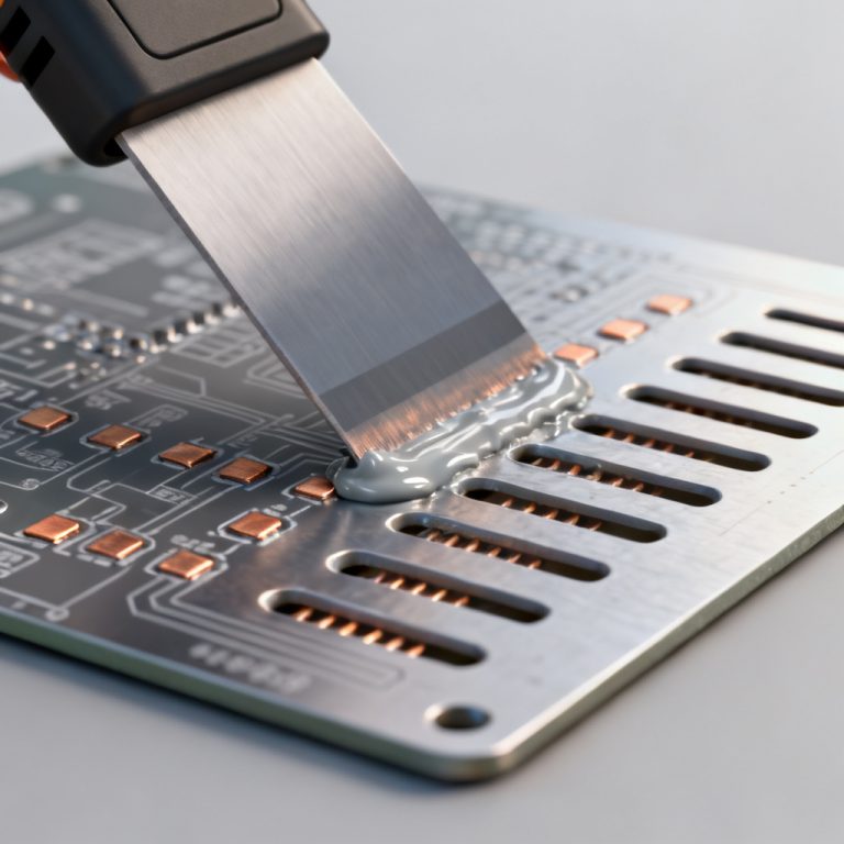
A stainless steel stencil is aligned over the bare PCB. Solder paste—a mixture of tiny solder spheres and flux—is applied and squeegeed across the stencil, depositing paste only where components will be placed. Stencil thickness, aperture size, and paste viscosity are meticulously controlled. For fine‑pitch components (e.g., 0.4 mm pitch BGAs), stencil design is paramount. Incorrect paste volume leads to shorts (bridges) or insufficient solder joints. Post‑printing, many high‑volume lines use Solder Paste Inspection (SPI) to measure paste height, volume, and area. This is a critical first step in defect prevention.
Step 2: Pick and Place
High‑speed pick‑and‑place machines use vacuum nozzles to pick components from tape‑and‑reel, tray, or tube feeders and place them onto the PCB with extreme accuracy. These machines can place up to 30,000+ components per hour (CPH) with accuracy down to ±25 microns (0.025 mm). Vision systems align components using fiducial marks on the PCB. SMDs include resistors, capacitors, ICs (QFP, QFN, BGA), LEDs, and connectors. The machine’s software must know the exact X‑Y coordinates and rotation for each component.
Step 3: Reflow Soldering
The PCB passes through a reflow oven with multiple heating zones. The solder paste melts (reflows), forming a permanent electrical and mechanical connection. A precise thermal profile is critical, consisting of four zones: Preheat – gradually heats the board and components; Soak (Dwell) – activates the flux, removing oxides; Reflow – peak temperature (typically 235–250 °C for lead‑free solder) where the solder melts; Cooling – controlled cooling solidifies the joints. Reflow is often performed in a nitrogen (N2) atmosphere to reduce oxidation and improve wetting, especially for fine‑pitch and BGA components.
Step 4: Cleaning (Optional but Recommended)
Flux residues can be conductive or corrosive over time, leading to electrical failures, especially in high‑reliability or high‑humidity environments. Methods include aqueous cleaning with deionized water and saponifiers, or solvent‑based cleaning. For no‑clean flux, cleaning may be omitted, but residues must be considered for conformal coating adhesion.
1.2 Advantages of SMT in PCB Assembly
- Higher Component Density: Components can be placed on both sides of the board.
- Smaller & Lighter: No holes or leads needed, allowing for miniaturization.
- Better High‑Frequency Performance: Shorter signal paths and lower parasitic inductance.
- Lower Cost per Component: Automated assembly is faster and more efficient.
- Easier Automation: Ideal for high‑volume production.
1.3 Common SMT Defects & Solutions
| Defect | Cause | Solution in PCB Assembly |
|---|---|---|
| Solder Bridges (Shorts) | Excess paste, misalignment, incorrect stencil design | Optimize stencil aperture, adjust placement accuracy |
| Tombstoning (Drawbridging) | Unbalanced pad designs, incorrect temperature profile | Balanced pad designs, correct reflow profile, uniform paste deposition |
| Solder Balls | Incorrect paste chemistry, improper reflow profile | Correct paste chemistry, proper reflow profile, adequate soak time |
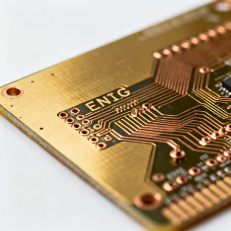
| Insufficient Solder | Low paste volume, poor pad finish | Increase paste volume, ensure good pad finish (e.g., ENIG) |
Through‑Hole Technology (THT) – The Robust Standard in PCB Assembly
PCB assembly using THT (or PTH – Plated Through‑Hole) involves inserting component leads through holes drilled in the PCB and soldering them to pads on the opposite side. It is older than SMT but remains essential for high‑reliability applications.
2.1 The THT Process: Step‑by‑Step
Step 1: Component Preparation & Insertion
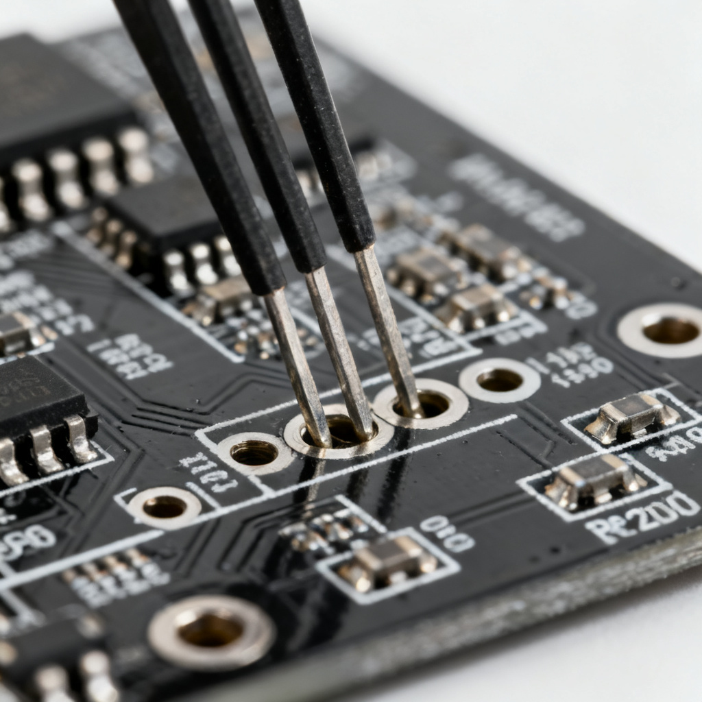
Manual Insertion: Used for low‑volume or complex assemblies. Operators hand‑place components (e.g., connectors, large capacitors, transformers) into the board. Auto‑Insertion (Axial & Radial): For high‑volume, specialized machines cut, form, and insert components automatically. Components are often loaded onto a tape or tube in a specific order for automated insertion.
Step 2: Soldering Methods
Wave Soldering (Most Common): The underside of the board is sprayed with flux, preheated, and then passed over a standing wave of molten solder. The solder wicks up through the plated holes and around the component leads, then solidifies during cooling. Selective Soldering: Used for boards with both SMT and THT components. A robotic nozzle precisely applies molten solder to individual THT joints, protecting sensitive SMT parts from the wave. Hand Soldering: For prototypes, rework, or low‑volume production, skilled operators use soldering irons.
Step 3: Lead Trimming (Clinching)
After soldering, excess lead lengths are trimmed close to the board surface. In some processes, leads are mechanically clinched (bent) against the pad before soldering to hold components in place during wave soldering.
2.2 Advantages of THT in PCB Assembly
- Superior Mechanical Strength: The lead‑through‑hole connection is physically stronger than SMT, ideal for components subject to vibration or stress (connectors, transformers, relays).
- High‑Power Handling: Can handle higher currents and dissipate more heat than SMT equivalents.
- Ease of Prototyping: Easier for manual assembly and rework.
- Reliability in Harsh Environments: Better for automotive, aerospace, and military applications.
2.3 Common THT Defects & Solutions
| Defect | Cause | Solution in PCB Assembly |
|---|---|---|
| Solder Bridges (Shorts) | Dense connectors, incorrect wave height | Use solder mask dams, adjust wave height, optimize board orientation |
| Insufficient Solder (Hole Fill) | Short wave contact time, poor flux activity | Increase wave contact time, improve flux activity, ensure proper preheat |
| Solder Voids | Incorrect flux chemistry, improper preheat | Optimize flux chemistry, adjust preheat profile |
| Component Lifting | Leads not clinched, adhesive missing | Ensure leads are properly clinched or use temporary adhesive |
Automated Optical Inspection (AOI) – The Quality Gate in PCB Assembly
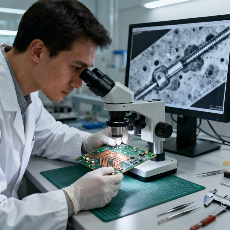
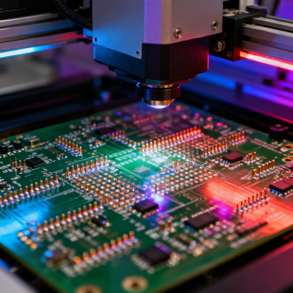
AOI is a non‑contact, vision‑based inspection system used after SMT reflow and after THT soldering to detect defects. It is the most common in‑line inspection method for PCB assembly.
3.1 How AOI Works
- Image Acquisition: High‑resolution cameras (often using multiple lighting angles – top, side, ring) capture images of the assembled board.
- Image Processing: The system compares the captured image to a “golden board” (a known‑good assembly) or to a CAD model/design data.
- Defect Detection: The software uses algorithms (e.g., pattern matching, color analysis, measurement) to identify anomalies. SMT defects detected: missing components, wrong component, tombstoning, solder bridges, insufficient solder, misalignment, polarity errors, lifted leads. THT defects detected: missing components, wrong component, insufficient hole fill, solder bridges, bent leads, component height issues.
- Reporting & Repair: The system flags defective boards and often generates a repair station with a high‑resolution image of the defect for an operator to verify and rework.
3.2 Types of AOI Systems
2D AOI: Inspects from above. Good for detecting missing/misaligned components and polarity. Less effective for solder joint quality. 3D AOI: Uses laser triangulation or structured light to create a 3D profile of the board. Critical for measuring solder joint height, volume, and shape. Essential for inspecting BGA and QFN hidden solder joints. Inline vs. Offline: Inline AOI is integrated into the production line for 100% inspection at production speed. Offline AOI is a standalone workstation for sampling or low‑volume inspection.
3.3 The Role of AOI in a PCBA Line
Post‑SMT Reflow: The most common placement. Catches SMT defects before the board moves to THT or final test. Post‑Wave/Selective Solder: Inspects THT joints for bridges, insufficient fill, and component presence. Final Inspection: Some lines use a final AOI to ensure no damage occurred during handling or secondary processes. Data for Yield Improvement: AOI software generates statistical data (e.g., Pareto charts of defect types). This data is fed back to the SMT line for continuous process improvement.
3.4 AOI vs. Other Inspection Methods
AOI vs. X‑Ray: AOI is for external, visible defects. X‑ray is for internal defects (e.g., BGA voids, hidden solder joints under shielded components, via fill). They are complementary, not alternatives. AOI vs. ICT (In‑Circuit Test): ICT is an electrical test that checks for shorts, opens, and component values. AOI is a visual test. AOI catches defects that ICT might miss (e.g., wrong component orientation), while ICT catches electrical failures that AOI cannot see. Both are used in a comprehensive test strategy.
Mixed Technology Assembly (SMT + THT) – The Best of Both Worlds in PCB Assembly
Most modern PCBs are mixed technology assemblies, combining SMT and THT components on the same board. The assembly process must be carefully sequenced.
4.1 The Typical Mixed‑Technology Process Flow
- Top‑Side SMT: Solder paste is printed on the top side. SMT components are placed. The board undergoes reflow soldering.
- Bottom‑Side SMT (Optional): If SMT components are on the bottom, they are glued to the board with a dot of adhesive before wave soldering to prevent them from falling off.
- THT Insertion: THT components (connectors, relays) are inserted into the board.
- Wave or Selective Soldering: The bottom side of the board is soldered. The glue holds the bottom‑side SMT components in place, and the wave solders the THT leads. The wave must not damage the top‑side SMT components.
- Inspection: AOI is typically performed after reflow and again after wave/selective soldering.
4.2 Design for Assembly (DFA) Considerations
- Component Spacing: Allow sufficient space between SMT components and THT holes to avoid shadowing during wave soldering.
- Orientation: Orient THT connectors so that leads are parallel to the wave direction to minimize bridges.
- Thermal Management: Large THT components (e.g., transformers) can act as heat sinks, requiring longer wave contact time or a preheater.
- Solder Mask: Use solder mask dams between THT pads to prevent bridges.
Quality & Reliability – Beyond AOI in PCB Assembly
While AOI is critical, a robust PCB assembly quality system involves multiple layers.
5.1 Other Inspection & Test Methods
- SPI (Solder Paste Inspection): The first line of defense.
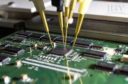
- ICT (In‑Circuit Test): A “bed of nails” fixture makes electrical contact with test points to check for shorts, opens, resistor/capacitor values, and diode orientation. Fast and reliable for volume production.
- Flying Probe Test: A slower, fixtureless alternative to ICT. Uses moving probes to test electrical points. Ideal for prototypes and low‑volume runs.
- Functional Test (FCT): Simulates the final operating environment of the PCB. Powers up the board and tests its actual functionality.
- Burn‑In Test: Running the board at elevated temperature and voltage for an extended period to identify early‑life failures.
5.2 Industry Standards & Certifications
- IPC‑A‑610: The most widely accepted standard for acceptability of electronic assemblies. Defines three classes: Class 1 (general electronic products), Class 2 (dedicated service electronics), Class 3 (high‑performance/harsh environment electronics).
- IPC‑J‑STD‑001: Requirements for soldered electrical and electronic assemblies.
- ISO 9001: Quality management system standard.
- AS9100: Aerospace quality management system standard.
- ISO 13485: Medical devices quality management system standard.
5.3 Common Failure Modes & Root Causes
- Solder Joint Fatigue: Caused by thermal cycling. Root cause: Coefficient of Thermal Expansion (CTE) mismatch between component and board.
- Electrochemical Migration (ECM): Growth of conductive metal filaments under bias and humidity. Root cause: Flux residues, ionic contamination.
- Pad Cratering: Cracks in the laminate under the copper pad. Root cause: Mechanical stress (board flex, drop impact), poor board material quality.
- Delamination: Separation of the copper foil from the laminate. Root cause: Thermal stress, moisture absorption, poor board quality.
Choosing the Right Assembly Partner – A B2B Perspective on PCB Assembly
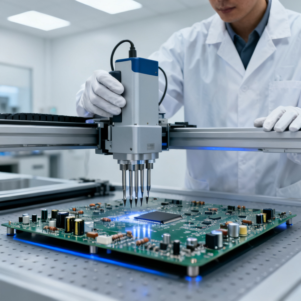
For B2B buyers, selecting a PCB assembly partner is a strategic decision. Key factors to evaluate:
6.1 Technical Capabilities
- Component Sourcing: Do they have a robust supply chain? Can they source hard‑to‑find or obsolete parts?
- Technology Range: Can they handle SMT, THT, mixed technology, BGA, fine‑pitch, and flex/rigid‑flex?
- Inspection & Test: Do they have in‑house AOI, X‑ray, ICT, and functional test? What is their defect rate (e.g., DPPM – Defective Parts Per Million)?
- Certifications: Are they IPC‑A‑610, ISO 9001, or AS9100 certified?
6.2 Production Flexibility
- Volume: Can they handle prototypes, low‑volume, and high‑volume runs?
- Lead Times: What are their standard and expedited lead times?
- NPI (New Product Introduction): Do they offer design‑for‑manufacturability (DFM) feedback to help optimize your design for lower cost and higher yield?
6.3 Communication & Transparency
- Customer Portal: Do they offer a portal to track order status, BOM costs, and quality reports?
- Engineering Support: Do they have experienced engineers who can answer technical questions and provide design recommendations?
- RMA (Return Material Authorization) Process: What is their process for handling defective units?
6.4 Cost Structure
- NRE (Non‑Recurring Engineering) Fees: Costs for setup, tooling, and programming.
- Unit Price: The cost per assembled board, which decreases with volume.
- Hidden Costs: Component procurement fees, testing fees, shipping.