Cleaning and Conformal Coating for PCB Protection
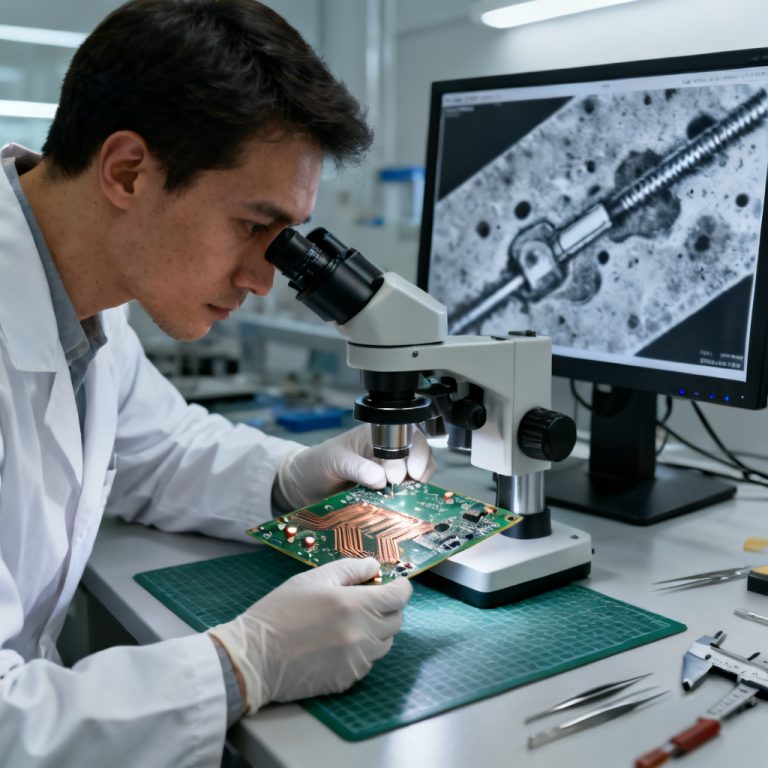
Proper Cleaning and Conformal Coating for PCB Protection is the cornerstone of long-term electronic reliability, preventing corrosion, electrochemical migration, and field failures. This pillar page consolidates best practices from IPC standards, Chemtronics, and leading manufacturers to help B2B engineers and procurement specialists ensure robust PCB performance in harsh environments.
This comprehensive resource covers the entire workflow—from contamination types and cleaning methods to coating selection, application, and verification—so you can implement a defect-free protection strategy.
Why Cleaning Matters for PCB Protection
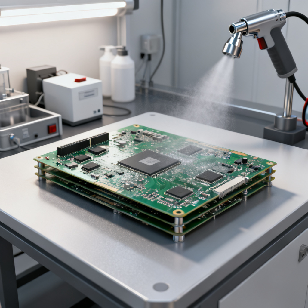
Contamination is the primary cause of premature PCB failure. Cleaning and Conformal Coating for PCB Protection are inseparable processes: without thorough cleaning, even the best coating will delaminate or trap corrosive residues. According to IPC J-STD-001 and industry leaders, residues from flux, solder balls, oils, and dust can lead to electrochemical migration (ECM), corrosion, and reduced surface insulation resistance (SIR).
Types of Contaminants Affecting PCB Protection
Understanding contaminants is the first step in effective Cleaning and Conformal Coating for PCB Protection. The table below summarizes the most common types:
| Contaminant Type | Common Sources | Risks to PCB Protection |
|---|---|---|
| Ionic | Flux activators, salts, human sweat | ECM, corrosion, SIR degradation |
| Non-Ionic | Rosin, oils, grease, silicone | Coating adhesion failure, outgassing |
| Particulate | Solder balls, dust, fibers | Short circuits, coating voids |
| Polar | Water-soluble flux residues | High conductivity, leakage |
Cleaning Methods for Optimal PCB Protection
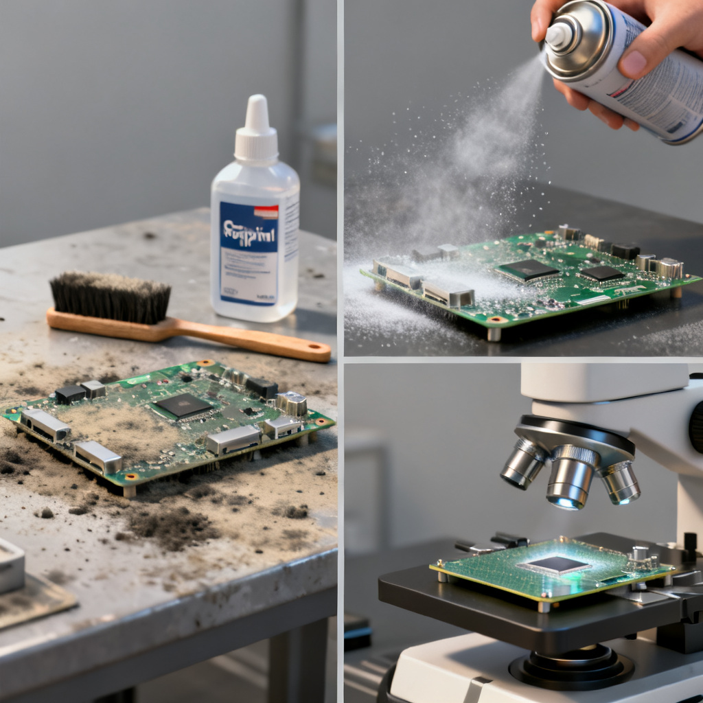
Choosing the right cleaning method is critical for Cleaning and Conformal Coating for PCB Protection. The following methods are endorsed by top industry sources:
- Aqueous Cleaning: Uses deionized water and saponifiers to remove water-soluble flux and ionic residues. Environmentally friendly, requires thorough rinsing (final resistivity ≥1 MΩ·cm per IPC).
- Solvent Cleaning (Vapor Degreasing): Non-aqueous solvents (e.g., modified alcohols, hydrofluoroethers) dissolve rosin-based flux and oils. Fast, leaves no residue, ideal for sensitive components.
- Semi-Aqueous Cleaning: Combines solvent wash (e.g., terpenes) with aqueous rinse. Effective for mixed contamination (rosin + water-soluble flux).
- Ultrasonic Cleaning: High-frequency cavitation dislodges contaminants from under BGAs and tight spaces. Use >40 kHz for fragile assemblies.
Cleaning Verification for PCB Protection
Verification ensures that Cleaning and Conformal Coating for PCB Protection meets reliability standards. Recommended tests include:
- Ionic contamination testing (IPC limit: ≤1.56 μg NaCl eq./in²).
- Surface Insulation Resistance (SIR) testing per IPC-TM-650.
- Visual inspection under UV light for fluorescent residues.
- Water drop test for hydrophobic residues.
Conformal Coating Types for PCB Protection
After cleaning, selecting the right conformal coating is essential for Cleaning and Conformal Coating for PCB Protection. The table below compares the six primary types:
| Coating Type | Key Properties | Best Applications | Limitations |
|---|---|---|---|
| Acrylic (AR) | Easy to apply, excellent moisture resistance, repairable | General-purpose, consumer electronics | Low chemical resistance |
| Urethane (UR) | Superior chemical and solvent resistance | Automotive, industrial | Difficult to repair, can be brittle |
| Silicone (SR) | Wide temperature range (-55°C to 200°C+), flexible | High-temperature, LED modules, aerospace | Low abrasion resistance, tacky |
| Epoxy (ER) | Outstanding hardness and dielectric strength | Military, medical implants | Very difficult to remove |
| Parylene (XY) | Ultra-thin (0.5–25 µm), pinhole-free | Medical devices, MEMS, sensors | Expensive, vacuum deposition required |
| Fluoropolymer (FP) | Extreme chemical resistance, low friction | Aerospace, fuel systems | Expensive, limited adhesion |
Application Methods for PCB Protection
Proper application is vital for Cleaning and Conformal Coating for PCB Protection. Methods include:
- Spray Coating: Fast, high-volume, requires masking of connectors and test points.
- Dip Coating: Uniform coverage for simple boards, but risks coating unwanted areas.
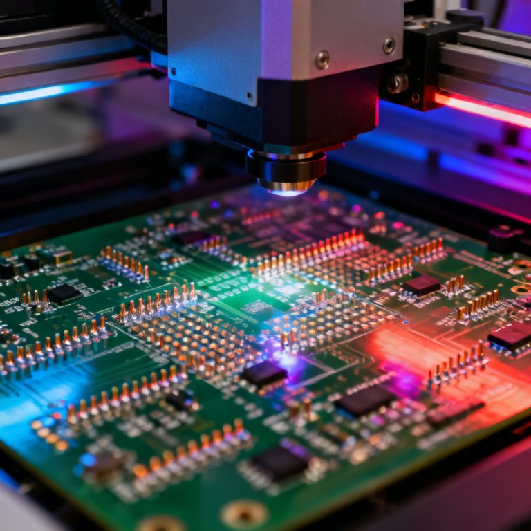
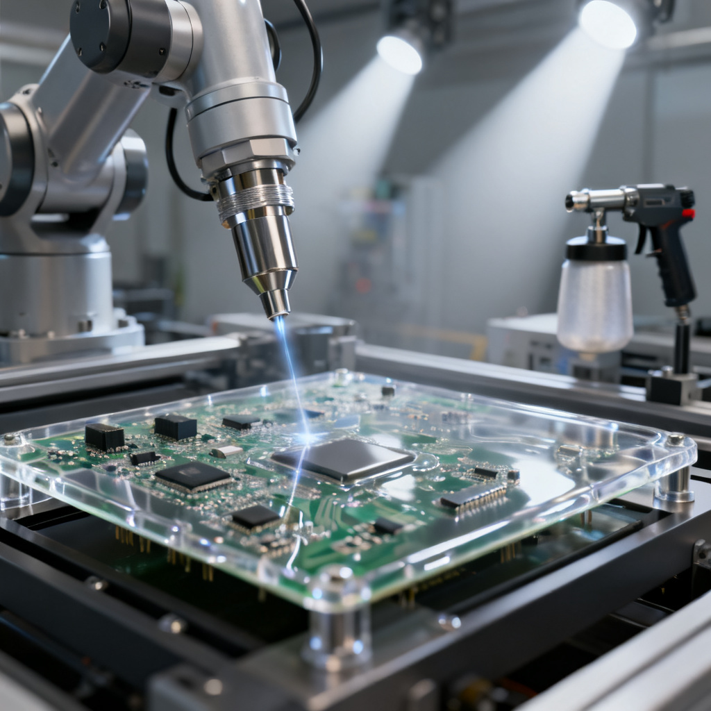
- Selective Coating: Robotic nozzles apply coating only to designated areas.
- Brush Coating: Manual, for prototypes or rework.
- Vapor Deposition (Parylene): Vacuum chamber process, perfect for all surfaces.
Pre-Coating Preparation: The Critical Step
All authoritative sources agree: Cleaning and Conformal Coating for PCB Protection fails if the surface is not properly prepared. Mandatory steps include:
- Clean the PCB using aqueous or solvent methods to achieve ≤1.56 μg NaCl eq./in².
- Dry thoroughly (bake at 60–80°C for 1–2 hours) to prevent blistering.
- Inspect for contamination via ionic testing or visual inspection.
- Mask all areas that must remain uncoated (connectors, test points, switches, LEDs, heatsinks).
Critical Warning: Never apply conformal coating over flux residues—they can react with the coating, causing delamination or electrochemical failure.
Curing and Quality Control for PCB Protection
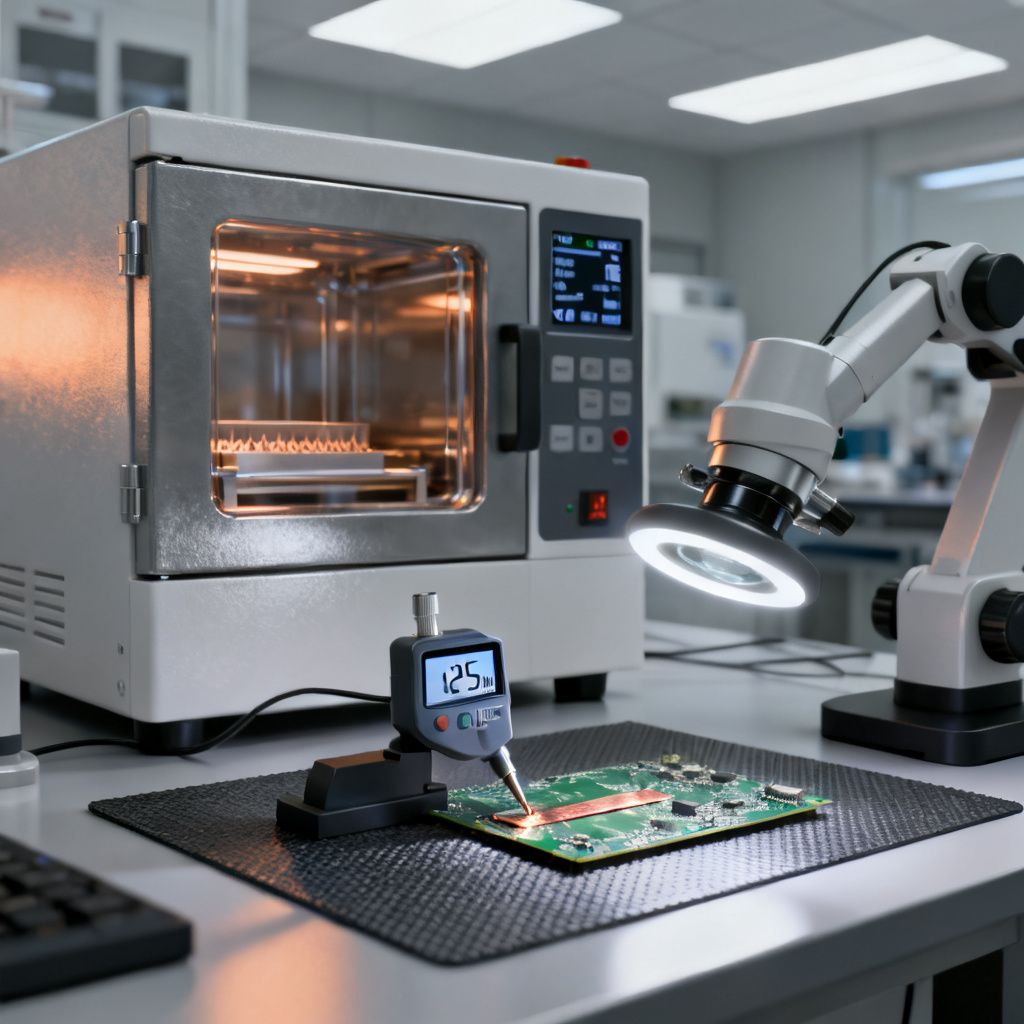
After application, curing must follow manufacturer specifications. Common methods: air drying (acrylics), thermal curing (urethanes, epoxies), UV curing, or moisture cure (silicones). Inspection includes:
- Visual check for voids, bubbles, and delamination.
- Thickness measurement (25–75 µm for most coatings, 0.5–25 µm for Parylene).
- Adhesion test (ASTM D3359 cross-hatch tape test).
- Dielectric withstand test (e.g., 500V for 1 minute).
- Thermal cycling (-40°C to +125°C) to check for cracking.
Best Practices and Common Pitfalls
Do’s for PCB Protection
- Always clean before coating—no exceptions.
- Use compatible materials (check coating chemistry with solder mask and components).
- Perform a test run on a sample board.
- Maintain a controlled environment (cleanroom class 100,000 or better).
- Document every step: cleaning method, coating type, thickness, cure profile, inspection results.
Don’ts for PCB Protection
- Apply coating over wet or damp boards.
- Use silicone coatings where rework is needed (hard to remove).
- Assume “no-clean” flux is safe—it can still cause adhesion failure.
- Forget to mask sensitive components (crystal oscillators, relays, connectors).
- Ignore rework guidelines.
Common Failures and Root Causes
| Failure | Root Cause | Solution |
|---|---|---|
| Coating delamination | Contamination under coating | Improve cleaning process |
| Bubbles/blisters | Trapped moisture or solvent | Pre-bake boards, use proper cure profile |
| Cracking (thermal) | Coating too thick or brittle | Use flexible coating or reduce thickness |
| Corrosion under coating | Ionic residues | Use ionic contamination testing |
| Poor adhesion | Incompatible coating or surface energy | Test adhesion; consider plasma treatment |
Standards for PCB Protection
To build trust with B2B buyers, reference these standards:
- IPC J-STD-001: Requirements for Soldered Electronic Assemblies.
- IPC-A-610: Acceptability of Electronic Assemblies.
- IPC-CC-830: Qualification of Conformal Coatings.
- MIL-I-46058C: Military specification for conformal coatings.
- UL 746E: Polymeric materials for electrical insulation.
Integrated Workflow for Maximum PCB Protection
Based on the most comprehensive sources, follow this process flow:
- Design for coating (avoid exposed copper, sharp angles, tall components causing shadowing).
- Solder using low-splash flux (preferably water-soluble).
- Clean immediately after soldering (aqueous or solvent).
- Verify cleanliness (≤1.56 μg NaCl eq./in²).
- Dry (bake at 60–80°C for 1 hour).
- Mask connectors, test points, and non-coatable areas.
- Apply coating (select method based on complexity and volume).
- Cure per manufacturer’s time/temperature profile.
- Inspect (visual, thickness, adhesion, dielectric tests).
- Final functional test and thermal cycling if required.
Frequently Asked Questions about Cleaning and Conformal Coating for PCB Protection
What is the most critical step in Cleaning and Conformal Coating for PCB Protection?
Can no-clean flux be used with conformal coating for PCB protection?
What is the recommended thickness for conformal coating in PCB protection?
How do I verify that cleaning is sufficient before conformal coating?
Which conformal coating type is best for high-temperature PCB protection?
Why Our PCB Protection Services Stand Out
Our Cleaning and Conformal Coating for PCB Protection services are IPC-compliant and backed by rigorous quality control. Unlike generic providers, we offer:
- Comprehensive cleaning verification (ionic, SIR, visual).
- Custom coating options (acrylic, urethane, silicone, Parylene).
- Full traceability and certification for each batch.
- Expert masking and selective coating for complex assemblies.
- Thermal cycling and dielectric testing as standard.
We maintain a neutral, professional tone and do not disparage competitors—our advantage lies in our documented processes and customer satisfaction.
Glossary of Terms for PCB Protection
- Electrochemical Migration (ECM): Formation of conductive metal filaments across a PCB surface under bias, caused by ionic contamination.
- Surface Insulation Resistance (SIR): Electrical resistance between adjacent conductors on a PCB surface, degraded by ionic residues.
- Outgassing: Release of trapped gases (e.g., moisture or solvents) from under a conformal coating, causing blisters.
- Delamination: Separation of conformal coating from the PCB surface due to poor adhesion or contamination.
- Dielectric Withstand Test: High-voltage test to verify insulation integrity of the coated assembly.