Stackup Design Layer Count Material Thickness
Stackup Design is the foundation of any high-performance PCB. This guide:Stackup Design Layer Count Material Thickness covers layer count, material selection, and thickness to help you achieve optimal signal integrity, thermal management, and cost efficiency.
Layer Count in Stackup Design
Layer Count Basics
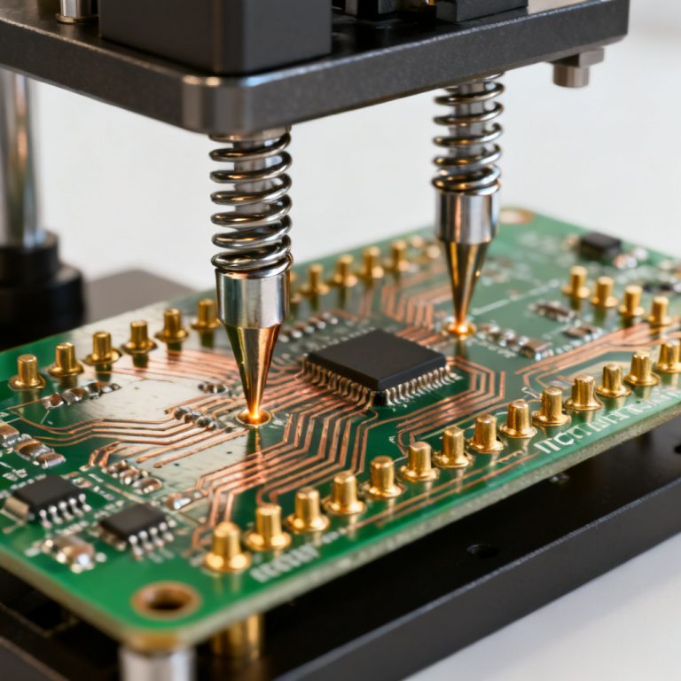
Stackup Design layer count refers to the number of conductive copper layers in a PCB. Common configurations include 2-layer, 4-layer, 6-layer, 8-layer, and beyond. The choice depends on circuit complexity, signal routing density, and EMI requirements. A 2-layer board is cost-effective for simple designs (e.g., power supplies or low-speed digital), but it offers limited routing space and poor noise isolation. In contrast, multi-layer boards (4+ layers) provide dedicated power and ground planes, reducing crosstalk and improving signal integrity.
Key Considerations for Layer Count Selection
- Signal Integrity: For high-speed signals (e.g., DDR, PCIe, or RF), a minimum of 4 layers is recommended. This allows a ground plane adjacent to signal layers, controlling impedance and minimizing loop inductance.
- Power Distribution: More layers enable separate power planes (e.g., 3.3V, 5V, and GND), reducing voltage drop and noise. For complex designs, 6-8 layers are typical.
- Thermal Management: Higher layer counts improve heat dissipation by distributing thermal load across multiple copper planes. For high-power applications, consider 8+ layers with thermal vias.
- Cost vs. Performance: Each additional layer increases fabrication cost by 20-30%. However, for prototypes or low-volume production, 4-6 layers balance cost and performance. For high-volume runs, optimize layer count to avoid over-engineering.
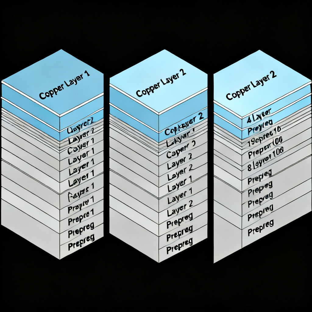
Advanced Layer Stackup Strategies
- Symmetry: Always maintain a symmetric stackup (e.g., even number of layers) to prevent warpage during lamination. Asymmetric stackups (e.g., 3 layers) are possible but require careful material balancing.
- Layer Ordering: Place critical signal layers adjacent to ground planes. For example, in a 6-layer stackup: Top (signal) – GND – Signal – Power – GND – Bottom (signal). This minimizes EMI and ensures controlled impedance.
- Blind and Buried Vias: For high-density designs (e.g., HDI), use blind vias (connecting outer to inner layers) and buried vias (connecting inner layers only) to save space. This increases layer count but reduces board size.
Material Selection in Stackup Design
Common PCB Materials
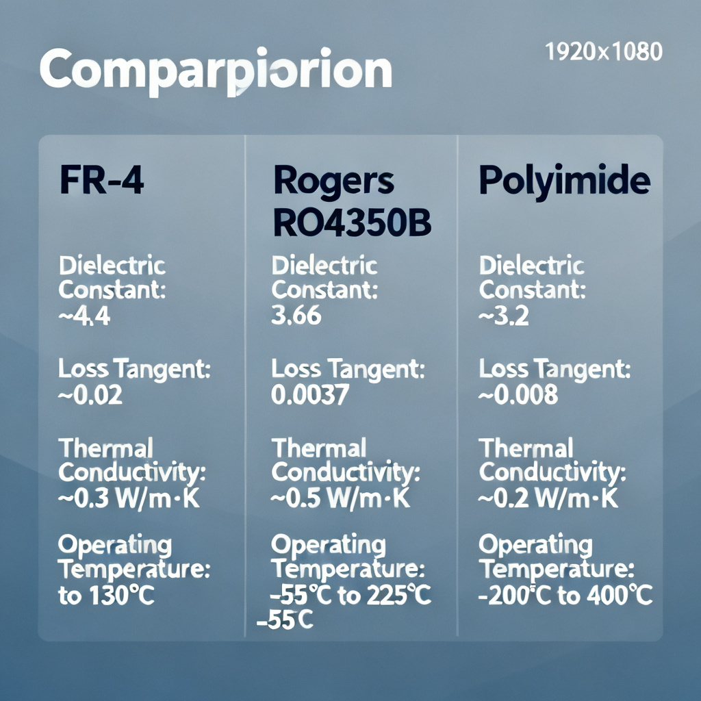
The substrate material (e.g., FR-4, high-Tg FR-4, Rogers, or polyimide) directly impacts electrical, thermal, and mechanical properties. Each has trade-offs:
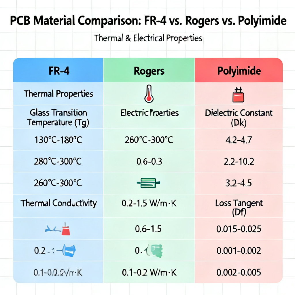
- FR-4: Standard epoxy-glass laminate, suitable for most digital and low-frequency analog designs. It offers good mechanical strength and cost-effectiveness (Tg ~130-140°C).
- High-Tg FR-4: For high-temperature applications (e.g., automotive or industrial), use materials with Tg >170°C (e.g., Isola 370HR or Shengyi S1000-2). This prevents delamination during soldering or operation.
- Rogers Materials: For RF/microwave designs (e.g., 5G or radar), use Rogers 4000 series (e.g., RO4350B) with low dielectric loss (Df <0.004) and stable Dk (3.48). They are expensive but essential for high-frequency performance.
- Polyimide: For flexible or high-reliability designs (e.g., aerospace or medical), polyimide (e.g., Kapton) offers thermal resistance up to 300°C and excellent flexibility.
Key Material Properties to Evaluate
- Dielectric Constant (Dk): Affects signal propagation speed and impedance. For controlled impedance, ensure consistent Dk across the board (e.g., FR-4 Dk = 4.2-4.8, Rogers Dk = 3.0-3.5). Lower Dk reduces signal delay.
- Dissipation Factor (Df): Measures signal loss. For high-speed digital, Df should be <0.02 at 1 GHz. For RF, target Df <0.001 (e.g., Rogers RO3003).
- Thermal Conductivity: For power electronics, use materials with high thermal conductivity (e.g., aluminum-backed or ceramic-filled substrates). Standard FR-4 has ~0.3 W/mK, while metal-core PCBs (MCPCBs) exceed 1.5 W/mK.
- CTE (Coefficient of Thermal Expansion): Match CTE of copper (17 ppm/°C) to prevent stress. High-Tg FR-4 has lower Z-axis CTE, reducing via failures.
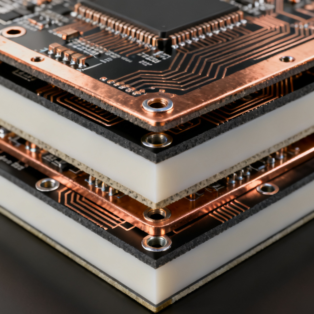
Material Stackup Combinations
- Hybrid Stackups: Combine FR-4 with Rogers for cost-effective high-frequency designs. For example, use Rogers for top signal layers and FR-4 for inner power planes. This reduces cost while maintaining RF performance.
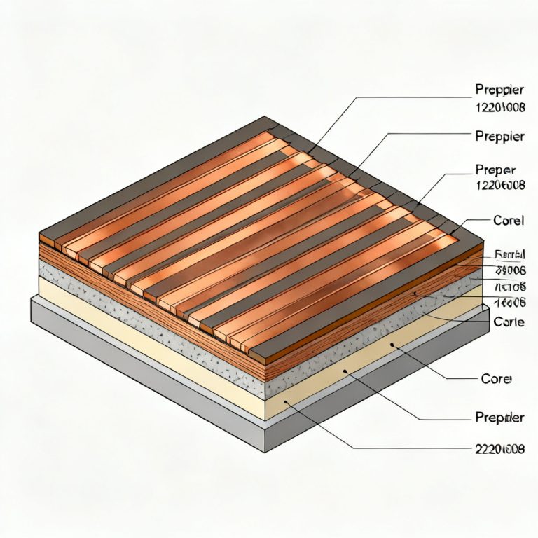
- Prepreg and Core: In multi-layer boards, alternate prepreg (bonding sheets) and core layers. For impedance control, select prepreg with the same Dk as the core. Common prepregs include 106, 1080, and 2116 (thickness varies from 0.05mm to 0.2mm).
Thickness in Stackup Design
Overall Board Thickness
Standard PCB thickness ranges from 0.6mm to 3.2mm, with 1.6mm being the most common. Thinner boards (0.8mm-1.0mm) are used for compact designs (e.g., mobile devices), while thicker boards (2.4mm-3.2mm) handle high current or mechanical strength. For multi-layer boards, thickness is determined by layer count and material thickness. A 4-layer board typically has a total thickness of 1.6mm (using 0.2mm core + 1.2mm prepreg + 0.2mm core).
Copper Weight (Thickness)
Copper thickness is measured in ounces per square foot (oz). Standard options:
- 1 oz (35 µm): For most digital and low-current analog designs.
- 2 oz (70 µm): For high-current applications (e.g., power supplies or motor drivers) to reduce resistance and heat.
- 0.5 oz (17.5 µm): For fine-pitch traces (e.g., 0.4mm BGA) to improve etching accuracy.
- Heavy Copper (3 oz to 10 oz): For industrial or automotive power circuits; requires wider trace spacing due to etching limitations.
Impedance Control and Thickness
- Microstrip and Stripline: For controlled impedance (e.g., 50Ω single-ended or 100Ω differential), adjust trace width, copper thickness, and dielectric height. Thinner dielectrics (e.g., 0.1mm) allow narrower traces for high-density routing.
- Impedance Calculation: Use tools like Polar SI8000 or IPC-2141 formulas. For example, a 50Ω microstrip on FR-4 (Dk=4.5) with 1 oz copper requires a trace width of 0.18mm for a 0.1mm dielectric height.
- Tolerance: Maintain ±10% impedance tolerance. For RF designs, tighten to ±5% using controlled materials (e.g., Rogers with <2% Dk variation).
Thickness for Specific Applications
- High-Speed Digital: Use thin dielectrics (0.1mm-0.2mm) between signal and ground layers to reduce loop inductance. For 100Ω differential pairs, target a dielectric thickness of 0.15mm.
- Power Electronics: Increase copper weight (e.g., 2 oz) and board thickness (e.g., 2.4mm) to handle 10A+ currents. Add thermal vias to dissipate heat.
- RF/Microwave: Use low-loss materials (e.g., Rogers RO4350B) with consistent thickness (e.g., 0.254mm or 0.508mm) to maintain Dk stability.
Advanced Stackup Design Practices
Signal Integrity and EMI Mitigation
- Return Paths: Ensure every signal layer has an adjacent ground plane (within 0.2mm) for low-inductance return paths. Avoid splits in ground planes.
- Decoupling Capacitors: Place capacitors close to power pins, using low-inductance vias (e.g., 0.2mm diameter). For high-frequency noise, use embedded capacitors in inner layers.
- EMI Shielding: Use ground planes on outer layers (e.g., top and bottom) to shield internal signals. For sensitive circuits, add a Faraday cage with stitching vias.
Thermal Management in Stackup
- Thermal Vias: Use arrays of vias (e.g., 0.3mm diameter, 1mm pitch) under hot components to transfer heat to inner ground planes. Fill vias with thermally conductive epoxy.
- Copper Pour Areas: Add large copper pours on top and bottom layers for heat spreading. Connect to ground planes via multiple vias.
- Material Selection: For high-power LEDs or IGBTs, use metal-core PCBs (MCPCBs) with aluminum base (1.5mm-3mm) and thin dielectric (0.1mm) for optimal thermal conductivity.
Manufacturability and DFM Rules
- Minimum Trace/Space: For standard FR-4, use 0.15mm/0.15mm (6 mil/6 mil). For HDI, reduce to 0.1mm/0.1mm (4 mil/4 mil) with laser-drilled vias.
- Via Size: Mechanical vias require 0.3mm minimum diameter; laser vias can be 0.1mm. For buried vias, ensure alignment within ±0.05mm.
- Panel Utilization: Design stackup to fit standard panel sizes (e.g., 18” x 24”) to reduce waste. Avoid odd layer counts to prevent bowing.
Cost Optimization Strategies
- Reduce Layer Count: Use high-density routing (e.g., via-in-pad or microvias) to achieve 2-layer designs where possible.
- Material Substitution: Replace Rogers with high-Tg FR-4 for non-critical RF layers. For prototypes, use standard FR-4 (e.g., TG130) instead of high-Tg.
- Standard Thicknesses: Stick to 1.6mm or 0.8mm to avoid special tooling charges. Use 1 oz copper for most designs.
Comparison: FR-4 vs. Rogers for High-Frequency Stackup Design
| Parameter | FR-4 (Standard) | Rogers RO4350B |
|---|---|---|
| Dielectric Constant (Dk) | 4.2-4.8 (varies with frequency) | 3.48 (stable up to 10 GHz) |
| Dissipation Factor (Df) | 0.02 at 1 GHz | 0.004 at 10 GHz |
| Thermal Conductivity | ~0.3 W/mK | ~0.6 W/mK |
| Cost per sq. ft. | $0.50-$1.00 | $5.00-$10.00 |
| Best Application | Low-speed digital, general purpose | RF/microwave, 5G, radar |
FAQ: Stackup Design – Layer Count, Material, Thickness
What is the optimal layer count for a high-speed stackup design?
For high-speed signals, a stackup design with at least 4 layers is recommended to provide dedicated ground planes and controlled impedance.
How does material selection impact stackup design thickness?
Material selection affects thickness because different substrates (e.g., FR-4 vs. Rogers) have varying dielectric constants and thermal properties, influencing the overall board thickness and impedance control.
Can I use a hybrid stackup design to reduce cost?
Yes, a hybrid stackup design combining FR-4 for inner layers and Rogers for outer signal layers can reduce cost while maintaining RF performance.
What copper weight is best for power electronics in stackup design?
For power electronics, use 2 oz or heavier copper in your stackup design to handle high currents and reduce resistive losses.
How do I control impedance in a multi-layer stackup design?
Impedance control in a stackup design requires careful adjustment of trace width, copper thickness, and dielectric height, often using tools like Polar SI8000.
{ “@context”: “https://schema.org”, “@type”: “BreadcrumbList”, “description”: “Breadcrumb navigation for Stackup Design guide”, “itemListElement”: [ { “@type”: “ListItem”, “position”: 1, “name”: “Home”, “item”: “https://advancepcbs.com/” }, { “@type”: “ListItem”, “position”: 2, “name”: “Blog”, “item”: “https://advancepcbs.com/blog/” }, { “@type”: “ListItem”, “position”: 3, “name”: “Stackup Design Layer Count Material Thickness”, “item”: “https://advancepcbs.com/stackup-design-layer-count-material-thickness/” } ] }