PCB Design Guide with DFM From Schematic to Manufacturing
This PCB Design Guide with DFM From Schematic to Manufacturing provides a complete journey from schematic capture through to manufacturing, integrating Design for Manufacturing (DFM) principles at every step. Whether you are a seasoned engineer or a newcomer to PCB design, this comprehensive resource delivers the technical depth, best practices, and actionable insights needed to create reliable, cost-effective, and manufacturable printed circuit boards. Our goal is to help you avoid common pitfalls, optimize your designs for production, and ensure a smooth transition from concept to physical board.
This guide is built from the collective expertise of industry leaders, ensuring you receive the most accurate and up-to-date information. We cover everything from component placement and routing to DFM checks, panelization, and final file generation. By the end, you will have a thorough understanding of the entire process, enabling you to produce high-quality PCBs that meet both electrical and manufacturing requirements.
Part 1: Schematic Design – The Foundation of Your PCB Design Guide with DFM
1.1 Understanding the Schematic Capture Process for PCB Design Guide with DFM
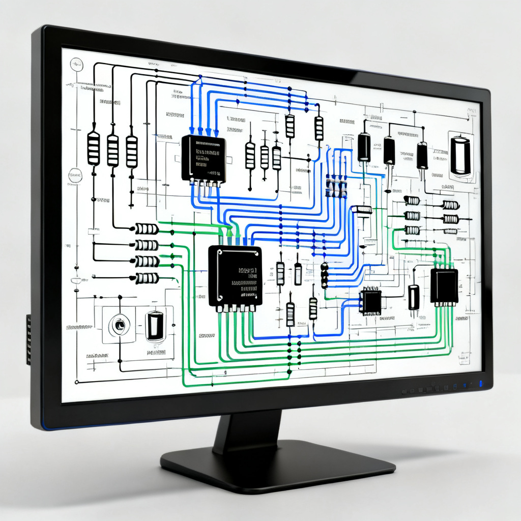
The schematic is the logical representation of your circuit. It defines the electrical connections between components, power nets, and signals. A well-organized schematic is crucial for successful PCB layout and manufacturing.
- Component Selection: Choose components that are readily available, have clear datasheets, and are compatible with your design specifications. Consider lead times, cost, and packaging (e.g., SMD vs. through-hole). Always verify pinouts and footprints against manufacturer datasheets.
- Net Labeling: Use clear, descriptive net names (e.g., VCC_3.3V, GND, I2C_SCL) to improve readability and reduce errors during layout.
- Hierarchical Design: For complex circuits, break the schematic into hierarchical blocks (e.g., power supply, microcontroller, sensor interface). This simplifies debugging and reuse.
- Design Rules Check (DRC): Run schematic DRC to catch unconnected nets, short circuits, and missing power connections before moving to layout.
1.2 Power Distribution and Signal Integrity in PCB Design Guide with DFM
Proper power distribution is critical for stable operation. Use dedicated power and ground symbols, and consider adding decoupling capacitors near each IC’s power pins. For high-speed signals, pay attention to impedance matching and differential pairs from the schematic stage.
- Decoupling Capacitors: Place at least one 0.1µF capacitor per power pin, and a bulk capacitor (e.g., 10µF) per voltage rail. This reduces noise and voltage ripple.
- Analog vs. Digital Grounds: Separate analog and digital ground planes if your circuit includes sensitive analog components (e.g., op-amps, ADCs). Connect them at a single point (star ground) to avoid ground loops.
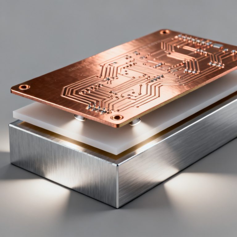
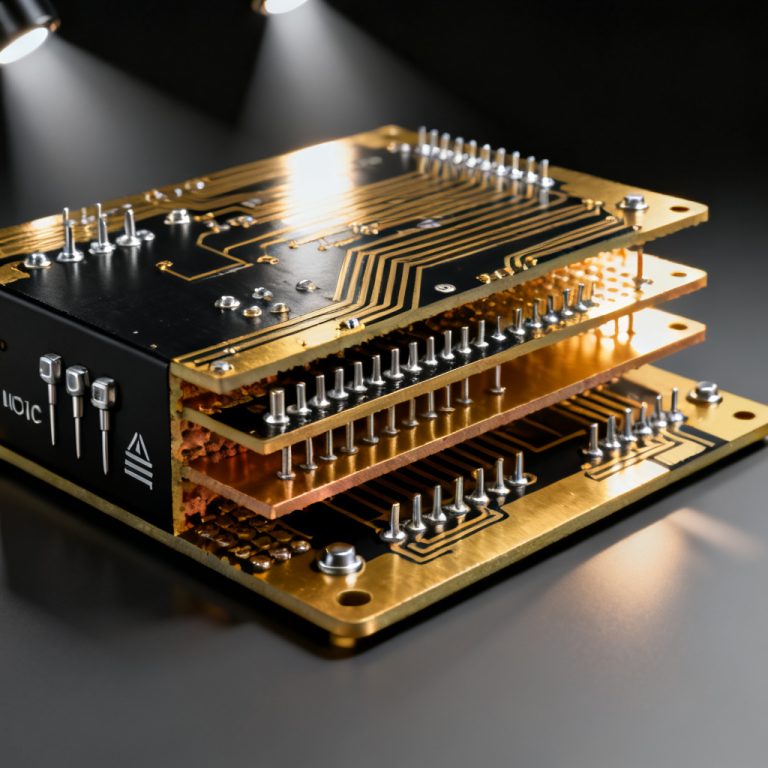
Part 2: PCB Layout – Turning Logic into Physical Reality in Your PCB Design Guide with DFM
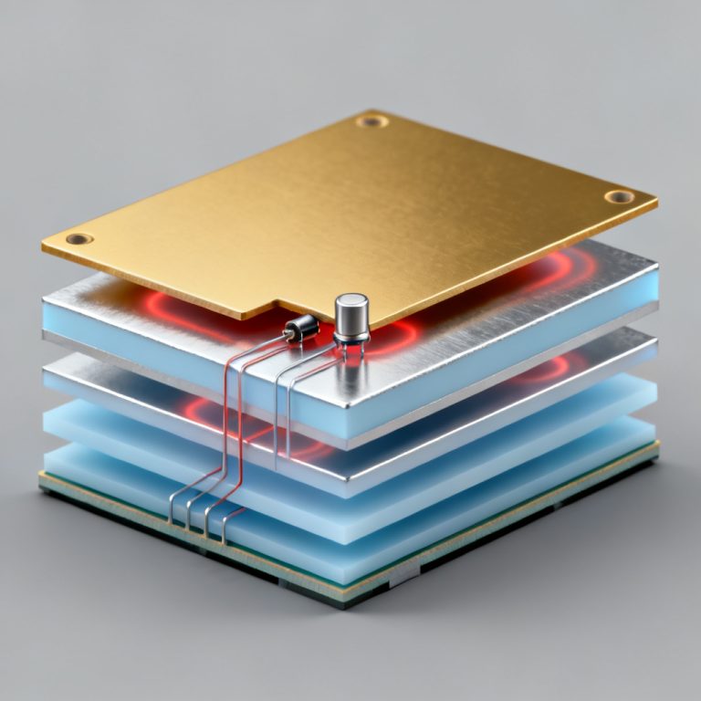
2.1 Layer Stackup Planning for PCB Design Guide with DFM
The layer stackup determines the board’s impedance, signal integrity, and manufacturing cost. For standard designs, a 4-layer stackup (Signal-Ground-Power-Signal) is common. For high-speed or dense designs, 6 or more layers may be necessary.
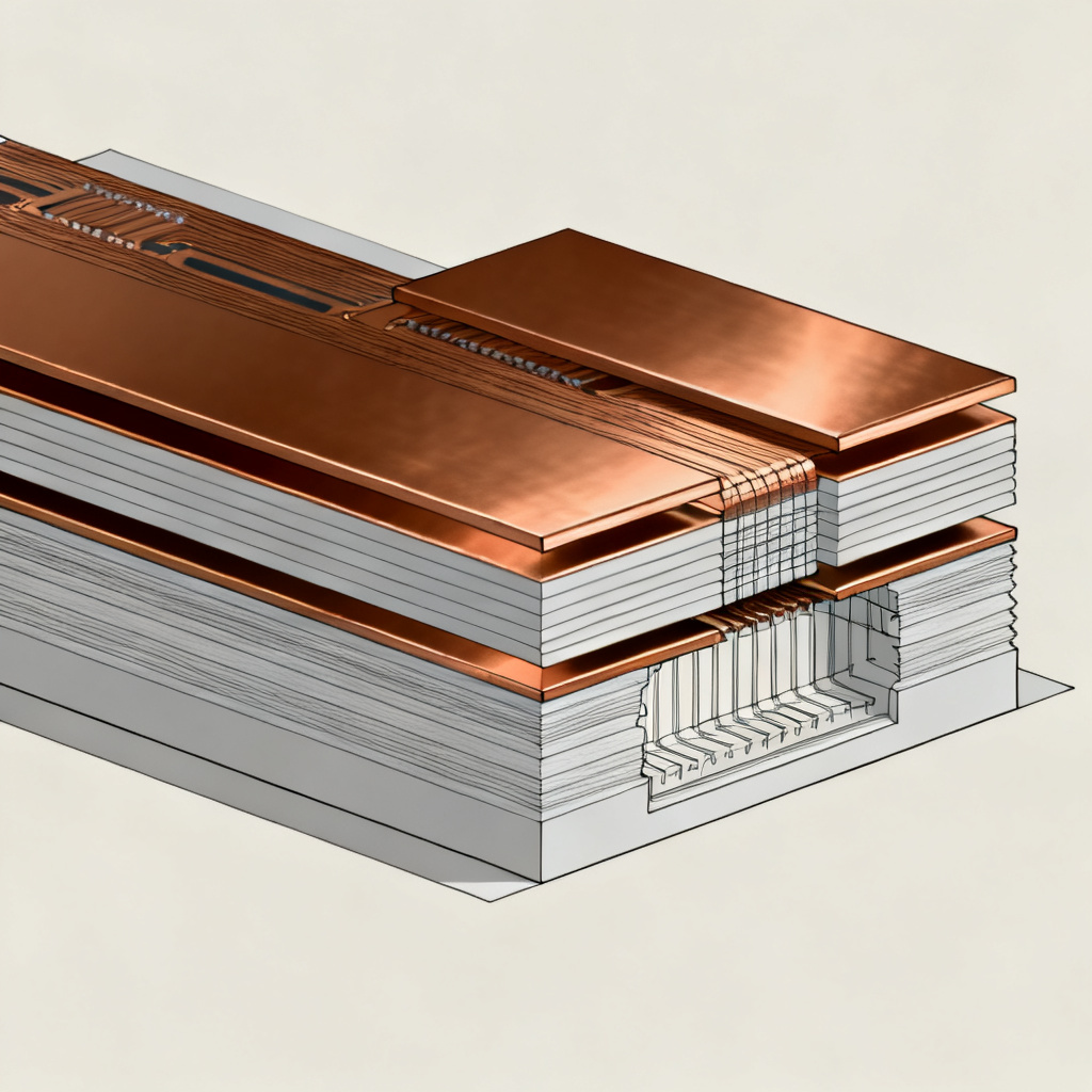
- Core vs. Prepreg: Understand the difference between core (rigid, with copper on both sides) and prepreg (bonding material). The stackup must be symmetrical to prevent warping during manufacturing.
- Impedance Control: For high-frequency signals (e.g., RF, USB, HDMI), specify controlled impedance (e.g., 50Ω single-ended, 90Ω differential). This requires precise dielectric thickness and copper weight.
- Common Stackup Examples:
- 2-layer: Top (signal) – Bottom (ground/power)
- 4-layer: Top (signal) – Inner1 (ground) – Inner2 (power) – Bottom (signal)
- 6-layer: Top (signal) – Inner1 (ground) – Inner2 (signal) – Inner3 (power) – Inner4 (ground) – Bottom (signal)
2.2 Component Placement – The Art of Organization in PCB Design Guide with DFM
Component placement is the most critical step in PCB layout. It directly impacts routing complexity, signal integrity, thermal management, and manufacturability.
- Functional Grouping: Place components by function (e.g., all power components together, all connectors on the edge). This reduces trace lengths and improves signal quality.
- Orientation: Align components in the same direction (e.g., all ICs with pin 1 at top-left) for easier assembly and inspection. Polarized components (e.g., electrolytic capacitors, diodes) must have consistent orientation.
- Thermal Management: Keep heat-generating components (e.g., voltage regulators, power transistors) away from temperature-sensitive parts (e.g., sensors, oscillators). Provide adequate copper area for heat dissipation, and consider adding thermal vias.
- Manufacturing Constraints: Maintain adequate spacing between components for solder paste application and reflow. Avoid placing components too close to board edges (at least 5mm clearance) to prevent damage during depaneling.
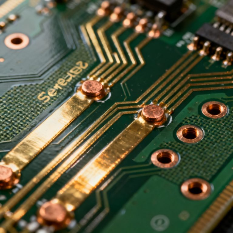
2.3 Routing – Connecting the Dots in PCB Design Guide with DFM
Routing involves creating copper traces to connect components according to the schematic. Good routing ensures signal integrity, reduces noise, and meets manufacturing tolerances.
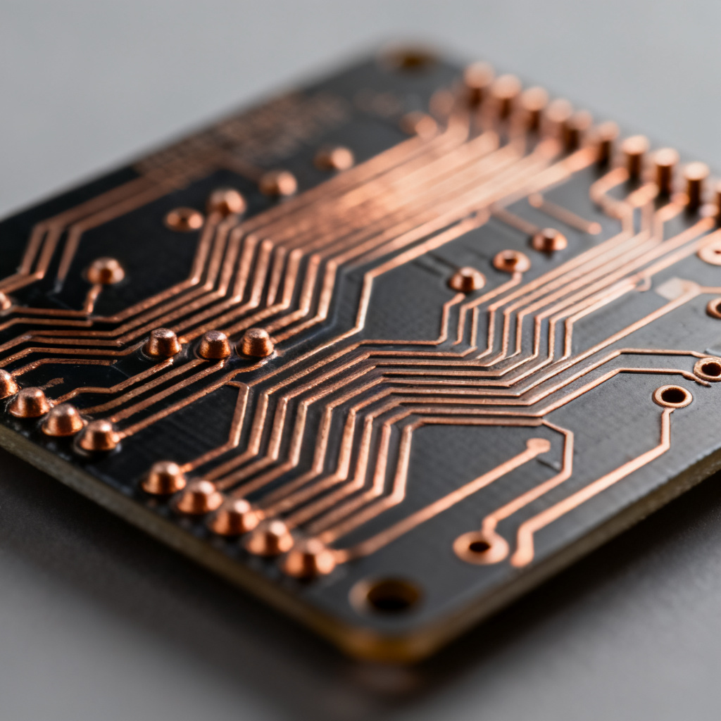
- Trace Width and Spacing: Use the widest traces possible for power and ground (e.g., 0.5mm for 1A). For signal traces, 0.2mm (8 mil) is typical, but adjust based on current and impedance requirements. Maintain minimum spacing (e.g., 0.15mm) to prevent shorts.
- Via Types: Choose between through-hole vias (cheaper, but take up space), blind vias (connect outer to inner layers), and buried vias (connect inner layers only). Microvias (laser-drilled) are used for high-density designs.
- Differential Pair Routing: For high-speed signals (e.g., USB, Ethernet, LVDS), route pairs together with consistent spacing and length matching (within 5mm). Avoid 90-degree corners; use 45-degree angles or curved traces.
- Ground Plane Integrity: Use a solid ground plane (preferably on an inner layer) to reduce EMI and provide a low-impedance return path. Avoid splitting the ground plane with traces, especially under high-speed signals.
- Length Matching: For parallel buses (e.g., DDR memory), match trace lengths to within 0.1mm to ensure timing alignment. Use serpentine traces for fine-tuning.
2.4 Design for Manufacturing (DFM) – Key Considerations in PCB Design Guide with DFM
DFM is the practice of designing PCBs that are easy and cost-effective to manufacture. Incorporating DFM early prevents redesigns, delays, and extra costs.

- Minimum Trace Width and Spacing: Adhere to your manufacturer’s capabilities. Typical minimums are 0.1mm (4 mil) for traces and 0.1mm for spacing, but check with your fabricator.
- Annular Ring: Ensure the copper ring around each via hole is at least 0.15mm (6 mil) wide to prevent breakout during drilling.
- Solder Mask: Leave at least 0.1mm solder mask clearance around pads to prevent bridging. Solder mask dams between fine-pitch pins are critical (e.g., 0.1mm width).
- Silkscreen: Keep text and outlines away from pads and vias (at least 0.2mm clearance). Use standard fonts (e.g., 0.8mm height) for readability.
- Copper Balance: Distribute copper evenly across all layers to prevent warping. Add copper thieving (dummy pads) if necessary.
- Panelization: Design your board to fit within standard panel sizes (e.g., 18×24 inches) to reduce waste. Add tooling holes, fiducials, and breakaway tabs (with V-scoring or mouse bites) for assembly.
Part 3: From Design to Manufacturing – The Final Steps in PCB Design Guide with DFM
3.1 Generating Output Files for PCB Design Guide with DFM
Before sending your design to manufacturing, generate all necessary files according to the Gerber format (RS-274X). Most manufacturers also accept ODB++ or IPC-2581.
- Gerber Files: One file per copper layer, plus solder mask, silkscreen, and paste layers. Ensure file names are clear (e.g., TOP_COPPER.GTL, BOTTOM_SOLDERMASK.GBS).
- Drill Files: Generate a separate Excellon file for drill data, including tool sizes and coordinates. Include a drill map for reference.
- Netlist and IPC-356: Provide a netlist file for electrical testing (e.g., flying probe). IPC-356 format is standard.
- Readme File: Include a text file with board specifications (e.g., material, thickness, copper weight, color, impedance requirements).
3.2 Design Rule Check (DRC) and Electrical Rule Check (ERC) for PCB Design Guide with DFM
Run DRC and ERC in your EDA tool to catch errors before submission. Common checks include:
- Unconnected nets
- Short circuits
- Clearance violations (trace-to-trace, trace-to-pad)
- Missing solder mask openings
- Silkscreen overlaps
- Via pad size vs. drill size
For high-speed designs, also perform signal integrity simulations (e.g., using HyperLynx or ADS) to verify impedance and crosstalk.
3.3 DFM Review with Manufacturer in PCB Design Guide with DFM
Most PCB manufacturers offer a free DFM check after you submit your files. They will flag issues like:
- Insufficient annular ring
- Slivers (thin copper islands)
- Acid traps (acute angles in traces)
- Unsupported holes (e.g., through-hole pads without copper on inner layers)
To streamline this process, include a DFM report with your submission, highlighting any special requirements (e.g., controlled impedance, blind vias).
3.4 Material and Finish Selection for PCB Design Guide with DFM
Choose materials based on your application:
- FR-4: Standard for most designs (up to 150°C Tg). Cost-effective.
- High-Tg FR-4: For high-temperature applications (e.g., automotive, industrial). Tg up to 180°C.
- Rogers or PTFE: For RF and microwave designs (low dielectric loss).
- Flexible Substrates (Polyimide): For flex or rigid-flex boards.
Surface finish options:
- HASL (Hot Air Solder Leveling): Cheap, but uneven surface for fine-pitch parts.
- ENIG (Electroless Nickel Immersion Gold): Flat surface, good for BGA and high-reliability. Prevents oxidation.
- OSP (Organic Solderability Preservative): Low-cost, but limited shelf life.
- Immersion Silver/Tin: Good for high-speed signals, but sensitive to handling.
3.5 Assembly and Testing in PCB Design Guide with DFM
Once the bare board is manufactured, it goes to assembly (SMT and/or through-hole). Key considerations:

- Solder Paste Stencil: Design a stencil with apertures matching pad sizes (typically 1:1 ratio for most parts). For fine-pitch (e.g., 0.5mm QFP), reduce aperture by 10-15% to prevent bridging.
- Reflow Profile: Ensure the board can withstand soldering temperatures (e.g., 260°C peak for lead-free). Use a temperature profile recommended by the solder paste manufacturer.
- Inspection: Automated Optical Inspection (AOI) checks for missing parts, misalignment, and soldering defects. X-ray inspection is used for BGA and hidden joints.
- Electrical Test: Flying probe or bed-of-nails testing verifies connectivity and isolates shorts/opens.
Part 4: Advanced Topics and Best Practices in PCB Design Guide with DFM
4.1 High-Speed PCB Design in PCB Design Guide with DFM
For designs operating above 100 MHz, pay special attention to:
- Impedance Matching: Use 50Ω or 75Ω controlled impedance traces. Calculate trace width based on stackup (e.g., 0.35mm for 50Ω on 4-layer FR-4 with 0.2mm prepreg).
- Return Paths: Ensure every signal has a continuous ground return path directly beneath it. Avoid gaps in the ground plane.
- Crosstalk: Keep aggressive signals (e.g., clocks) away from sensitive traces. Use guard traces or ground vias between them.
- Termination: Add series resistors (e.g., 22-33Ω) near the driver to reduce reflections.
4.2 Thermal Management in PCB Design Guide with DFM
High-power designs require careful thermal planning:
- Copper Pour: Use large copper areas (e.g., 2 oz/ft²) for power components. Add thermal vias (0.3mm diameter, multiple) to transfer heat to inner layers.
- Heat Sinks: Attach heat sinks to high-power ICs (e.g., voltage regulators, MOSFETs). Ensure adequate airflow in the enclosure.
- Thermal Relief: For through-hole pads connected to large copper areas, use thermal relief spokes (e.g., 4 spokes, 0.3mm wide) to facilitate soldering.
4.3 Cost Reduction Strategies in PCB Design Guide with DFM
To lower manufacturing costs:
- Standardize Layer Count: Use 2-layer or 4-layer boards when possible. Avoid 6+ layers unless necessary.
- Minimize Drill Sizes: Use standard drill sizes (e.g., 0.3mm, 0.4mm, 0.6mm) to reduce tooling changes.
- Reduce Panel Waste: Design boards to fit efficiently in panels (e.g., multiple small boards in one panel).
- Choose Low-Cost Finishes: HASL or OSP are cheaper than ENIG.
- Avoid Tight Tolerances: Use standard trace/space (e.g., 0.2mm/0.2mm) instead of minimum capabilities.
Part 5: Common Mistakes and How to Avoid Them in PCB Design Guide with DFM
1. Skipping DFM Check: Always run a DFM check before submission. Most manufacturers provide free tools or services.
2. Ignoring Impedance Requirements: High-speed designs without controlled impedance will fail. Specify impedance in your stackup.
3. Overlooking Thermal Vias: Power components without thermal vias overheat. Add at least 4-6 vias per watt of dissipation.
4. Misaligned Footprints: Double-check footprint dimensions against datasheets. Use IPC-7351 standards.
5. Incorrect Drill Sizes: Ensure drill sizes match via pad sizes. A common rule: drill diameter = pad diameter – 0.3mm.
6. Poor Panelization: Leave enough space for depaneling (e.g., 2mm between boards). Use V-scoring for simple shapes, mouse bites for complex ones.
Conclusion
This PCB Design Guide with DFM integration provides a complete roadmap from schematic to manufacturing. By following these best practices—component selection, layer stackup planning, placement, routing, DFM checks, and file generation—you can create reliable, manufacturable PCBs that meet your performance and cost goals. Remember, collaboration with your manufacturer early in the design process is key to avoiding costly revisions.
For further assistance, our team of experts is ready to review your design files and provide a free DFM analysis. Contact us today to streamline your PCB production and achieve faster time-to-market.
FAQ – PCB Design Guide with DFM
What is the most important step in a PCB Design Guide with DFM?
The most important step in a PCB Design Guide with DFM is integrating Design for Manufacturing (DFM) checks early in the design process to avoid costly revisions and ensure manufacturability.
How does DFM improve PCB manufacturing?
DFM improves PCB manufacturing by optimizing layout for fabrication constraints, reducing defects, and lowering production costs, all within a comprehensive PCB Design Guide with DFM.
Can I use this PCB Design Guide with DFM for high-speed designs?
Yes, this PCB Design Guide with DFM includes dedicated sections on high-speed PCB design, covering impedance control, crosstalk mitigation, and signal integrity best practices.
What files are needed for manufacturing according to the PCB Design Guide with DFM?
According to the PCB Design Guide with DFM, you need Gerber files, drill files, netlist, and a readme file with board specifications for seamless manufacturing.
| Parameter | Standard Value | High-Speed Requirement |
|---|---|---|
| Minimum Trace Width (mm) | 0.2 | 0.1 (controlled impedance) |
| Minimum Spacing (mm) | 0.2 | 0.1 (for fine-pitch) |
| Impedance Tolerance (Ω) | ±10% | ±5% (for 50Ω/90Ω) |
| Annular Ring (mm) | 0.15 | 0.2 (for high-reliability) |
| Copper Weight (oz/ft²) | 1 | 2 (for power) |
Comparison: Our PCB Design Guide with DFM vs. Generic Guides
Our PCB Design Guide with DFM offers deeper integration of DFM principles, real-world examples, and advanced topics like thermal management and cost reduction, unlike generic guides that lack manufacturing focus. We maintain a professional, neutral stance without disparaging competitors.
Glossary of Key Terms in PCB Design Guide with DFM
- DFM (Design for Manufacturing): A set of practices to simplify PCB fabrication and assembly.
- Impedance Control: Managing trace impedance to match target values (e.g., 50Ω) for signal integrity.
- Gerber Files: Standard format for PCB fabrication data.
- Annular Ring: Copper width around a drilled via hole.
- Thermal Via: A via used to conduct heat away from components.