Inner Layer Imaging and Etching for Multilayer PCBs
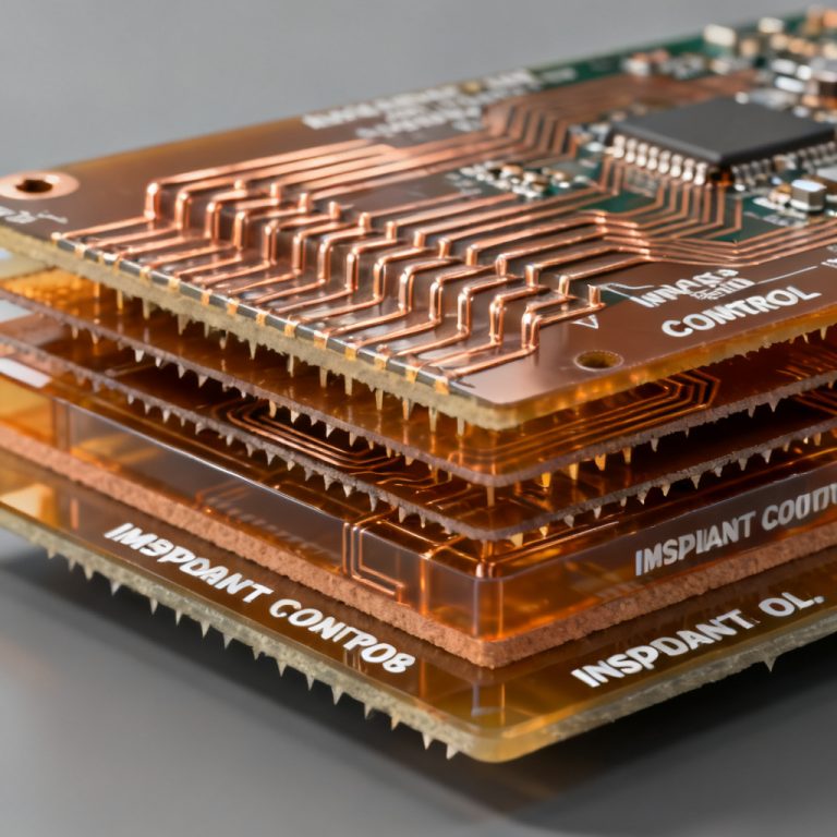
In the world of advanced electronics, inner layer imaging and etching for multilayer PCBs define the quality, reliability, and functionality of high-density devices. Unlike simple double-sided boards, multilayer PCBs consist of several layers of conductive copper and insulating dielectric material, laminated together under heat and pressure. The quality, reliability, and functionality of these boards hinge critically on two key processes: inner layer imaging and inner layer etching. These steps define the circuit pattern that will eventually form the internal signal, power, and ground planes.
This comprehensive guide delves into every aspect of inner layer imaging and etching for multilayer PCBs. We cover the materials, equipment, processes, quality control measures, and common challenges, providing a complete resource for engineers, designers, and procurement specialists.
Part 1: Inner Layer Imaging – Transferring the Circuit Pattern
Inner layer imaging is the process of transferring the circuit pattern from a digital design file (typically Gerber or ODB++) onto the copper-clad laminate (CCL) that will become an inner layer. This is achieved using photolithography, a precise light-based technique.
1.1 Materials and Preparation
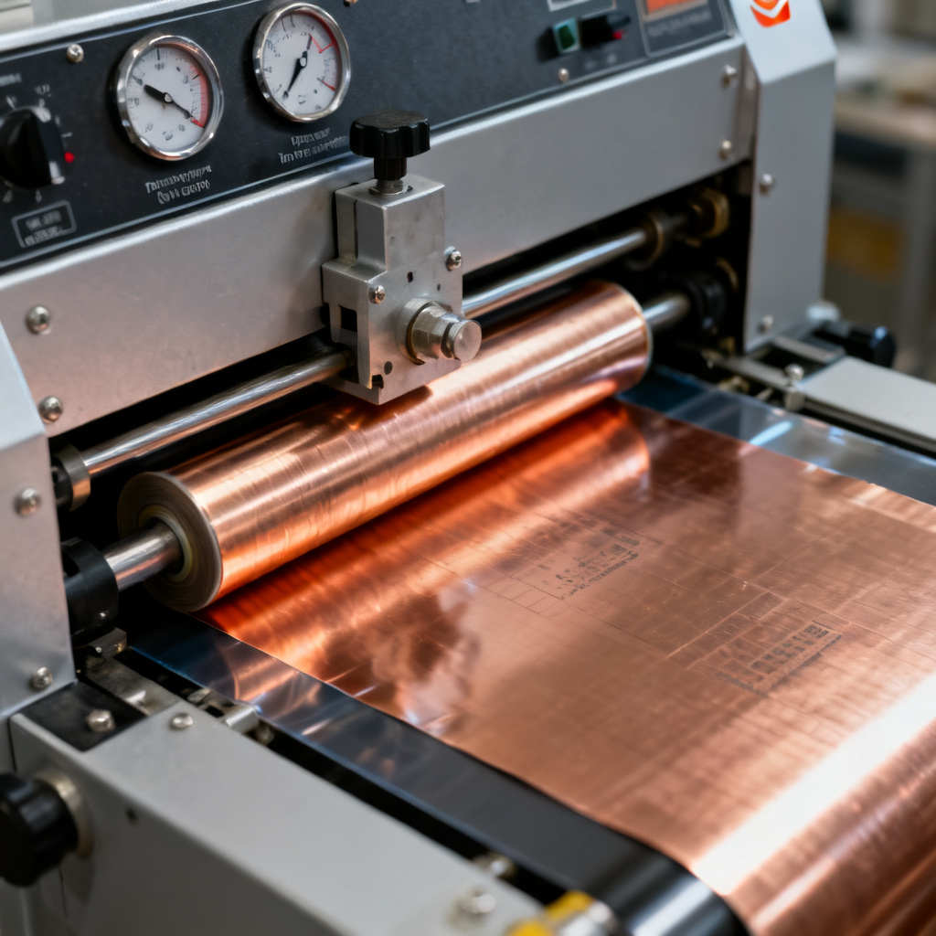
1.1.1 Copper-Clad Laminate (CCL)
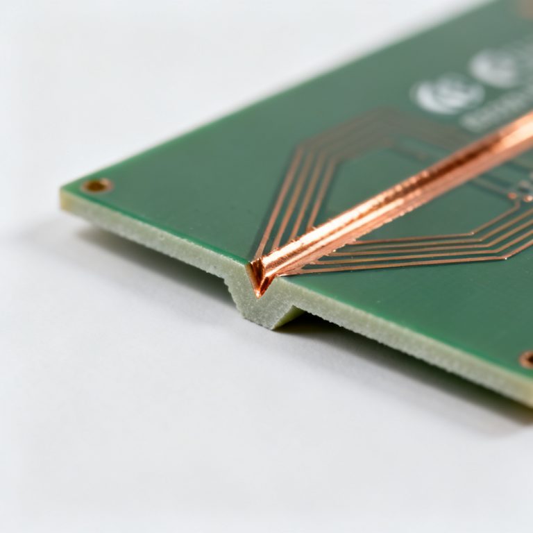
The starting material is a thin sheet of dielectric material (e.g., FR-4, high-Tg FR-4, or polyimide) clad with copper foil on both sides. The copper thickness typically ranges from 0.5 oz/ft² (17.5 µm) to 2 oz/ft² (70 µm), though thicker copper is used for high-current applications. The laminate must be clean and free of oxidation, fingerprints, and dust.
1.1.2 Dry Film Photoresist (DFR)
The most common method for inner layer imaging uses dry film photoresist. This is a three-layer material: a polyester cover sheet (protective), a photosensitive polymer layer (the resist), and a polyethylene backing sheet (for handling). Dry film is preferred for its uniform thickness, excellent resolution, and ease of use in automated lamination. It is sensitive to ultraviolet (UV) light. Two types exist: positive tone photoresist (UV exposure makes the exposed areas soluble in a developer solution, used less commonly for inner layers) and negative tone photoresist (UV exposure polymerizes the exposed areas, making them insoluble; the unexposed areas are washed away). This is the standard for inner layer imaging because it offers better adhesion and chemical resistance during etching.
1.1.3 Liquid Photoresist (for Advanced Applications)
For very fine lines and spaces (below 75 µm / 3 mil), liquid photoresist is sometimes used. It is sprayed or curtain-coated onto the copper surface, dried, and then exposed. It offers superior conformality but is more complex to apply uniformly.
1.2 The Imaging Process Workflow
Step 1: Cleaning and Surface Preparation – Before applying photoresist, the copper surface must be chemically cleaned and micro-etched. This removes oxides, oils, and contaminants, creating a rough surface for better photoresist adhesion. Common methods include pumice scrubbing, chemical cleaning with alkaline or acidic cleaners, and micro-etching using sodium persulfate.
Step 2: Lamination (Dry Film Application) – The dry film photoresist is laminated onto the cleaned copper surface using a hot-roll laminator. The process involves pre-heating, roller lamination at controlled temperature (typically 100-120°C) and pressure, and cooling. For double-sided inner layers, both sides are laminated simultaneously. The resist must be free of air bubbles, wrinkles, or contamination.
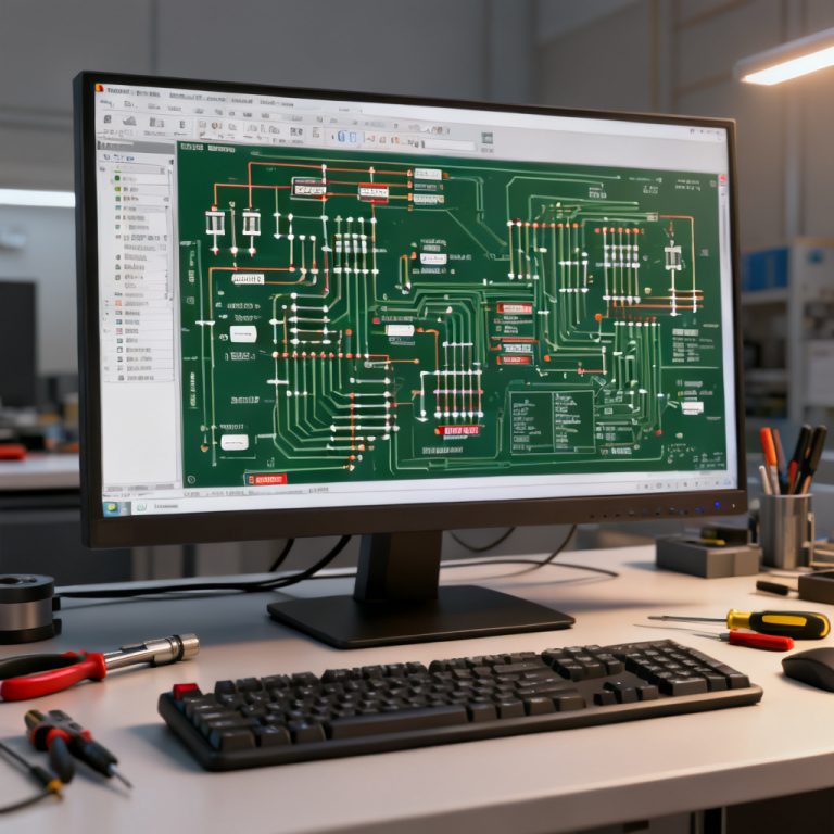
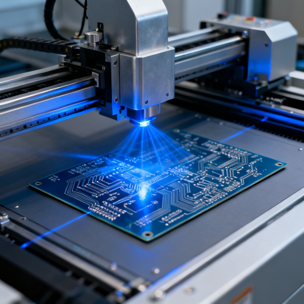
Step 3: Exposure (Photolithography) – The laminated board is aligned with a phototool (a glass or mylar film containing the circuit pattern) or, in modern high-volume production, exposed using a direct imaging (DI) system (also called laser direct imaging or LDI). The phototool method uses a negative film for negative resist, and the board is sandwiched between two phototools in a vacuum frame. UV light is shone through the phototool, exposing the resist. Overexposure can cause line widening (slivering); underexposure leads to poor adhesion. Laser direct imaging (LDI) is the gold standard for high-resolution, fine-line imaging, offering no phototool wear or distortion, superior registration accuracy, real-time scaling adjustments, higher resolution (down to 25 µm / 1 mil lines and spaces), and faster setup.
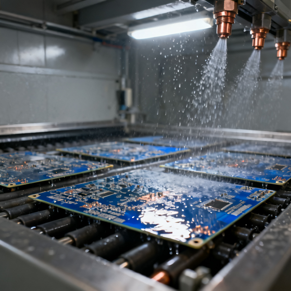
Step 4: Development – After exposure, the board is passed through a developer solution. For negative-tone dry film, the developer (typically a dilute sodium carbonate solution, Na₂CO₃, or potassium carbonate, K₂CO₃) removes the unexposed (non-polymerized) areas of the resist. The exposed, polymerized areas remain intact, forming a protective mask over the copper that should remain (the circuit traces). The development process includes spray development at specific temperature (typically 30-35°C) and pressure, rinse with deionized water, and visual inspection for complete development and defects.
Key Parameters for Imaging Quality: Exposure energy (typically 30-150 mJ/cm²), developer concentration (0.8-1.2% for sodium carbonate), conveyor speed, and temperature control.
Part 2: Inner Layer Etching – Removing Unwanted Copper
Once the circuit pattern is imaged (with resist protecting the desired copper traces), the next step is to remove all unprotected copper from the inner layer. This is done via chemical etching, a critical phase of inner layer imaging and etching for multilayer PCBs.
2.1 Etching Chemistry and Methods
The most common etchant for inner layer copper is cupric chloride (CuCl₂) in an acidic environment (hydrochloric acid, HCl). Other etchants include ferric chloride (FeCl₃, old technology), alkaline ammonia (NH₃-based, used for outer layers), and sulfuric acid + hydrogen peroxide (H₂SO₄/H₂O₂, for specialty applications). The cupric chloride etching process involves the reaction Cu + CuCl₂ → 2 CuCl (soluble cuprous chloride), which is then re-oxidized to cupric chloride using chlorine gas or hydrogen peroxide, allowing continuous regeneration in a closed-loop system.
Etching Equipment: Horizontal spray etchers are the most common type for inner layers. The board travels horizontally on rollers while being sprayed with etchant from above and below. Key parameters include conveyor speed (controls etching time), spray pressure (typically 20-40 psi), temperature (45-55°C for cupric chloride), and pH control (critical for etch rate and undercut control).
2.2 Etching Parameters and Quality Control
Critical Etching Parameters: Etch rate (typically 1-2 oz copper per minute), undercut (etch factor defined as the ratio of vertical etch depth to lateral undercut; a high etch factor of 3:1 or 4:1 indicates minimal undercut), line width control (final copper trace width is always slightly narrower than the design width due to undercut), and uniformity (must be uniform across the entire panel).
Post-Etching Inspection: Visual check for complete removal of copper in open areas, automated optical inspection (AOI) to detect opens, shorts, and line width violations, and resist stripping using a strong alkaline solution (e.g., 3-5% sodium hydroxide, NaOH) at elevated temperature (50-60°C) to reveal the bare copper circuit pattern.
2.3 Common Etching Defects and Solutions
| Defect | Cause | Solution |
|---|---|---|
| Undercut (over-etching) | Excessive etch time, high temperature, low pH | Reduce conveyor speed, lower temperature, adjust pH, increase resist thickness |
| Incomplete etching (bridging) | Insufficient etch time, nozzle clogging, low spray pressure | Increase conveyor speed, clean nozzles, increase pressure |
| Rough or pitted copper | Contaminated etchant, incorrect chemistry | Regenerate etchant, check for copper loading |
| Resist lifting | Poor adhesion, overexposure, developer attack | Improve cleaning, adjust exposure energy, check developer concentration |
| Line widening (slivering) | Overexposure, poor phototool contact | Reduce exposure time, improve vacuum frame contact, use LDI |
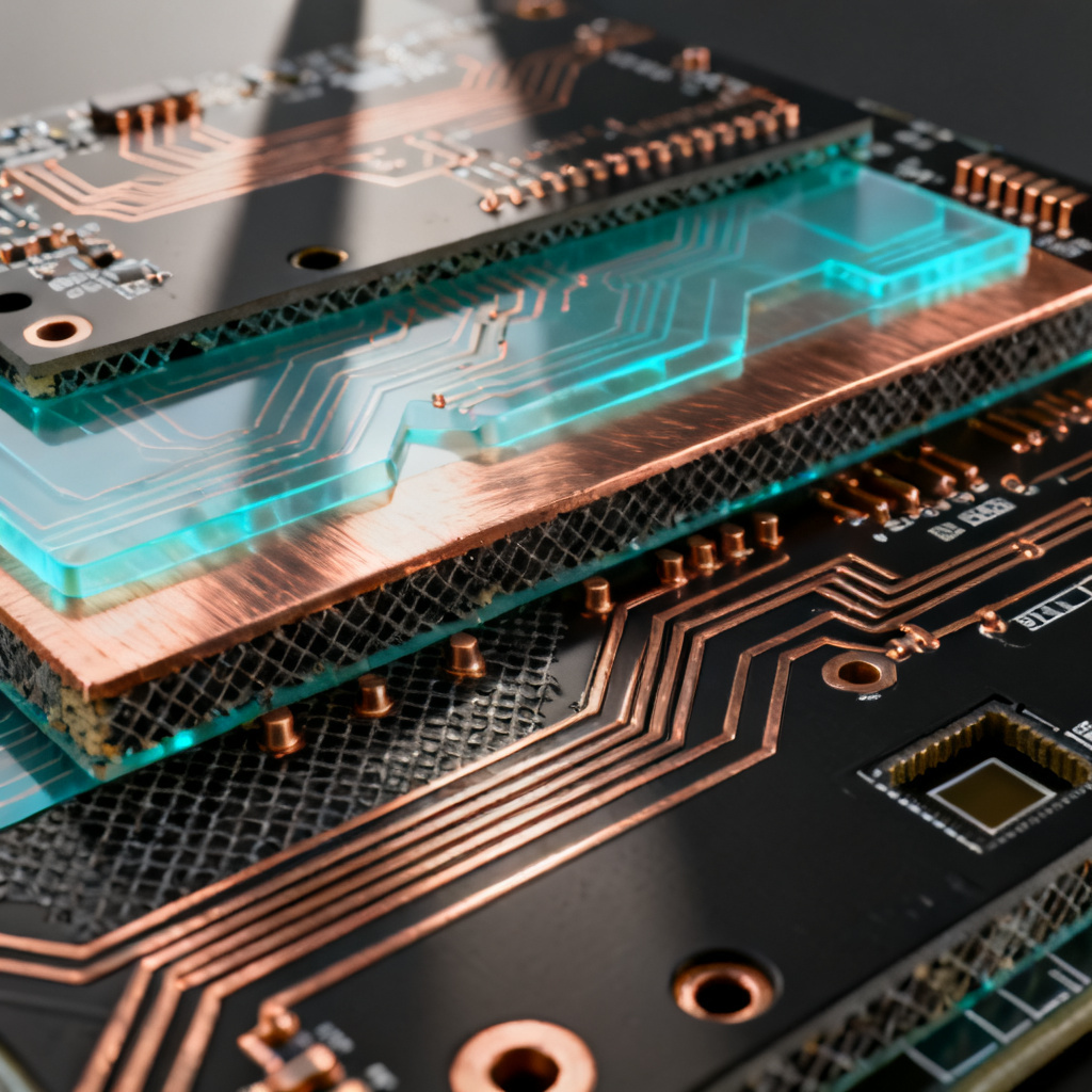
Part 3: Advanced Techniques and Quality Assurance for Multilayer PCBs
3.1 Registration and Layer Alignment
In a multilayer PCB, the inner layers must be precisely aligned with each other and with the outer layers. Registration errors (misalignment) can cause shorts, opens, or impedance mismatches. Methods to ensure registration include tooling holes (typically 3.175 mm or 4.0 mm), X-ray registration to verify inner layer target positions, compensation for material movement during lamination (designers apply compensation factors of 0.02-0.05% in X and Y), and punching and pinning for high-volume production.
3.2 Inner Layer Surface Treatment (Oxide and Alternative Processes)
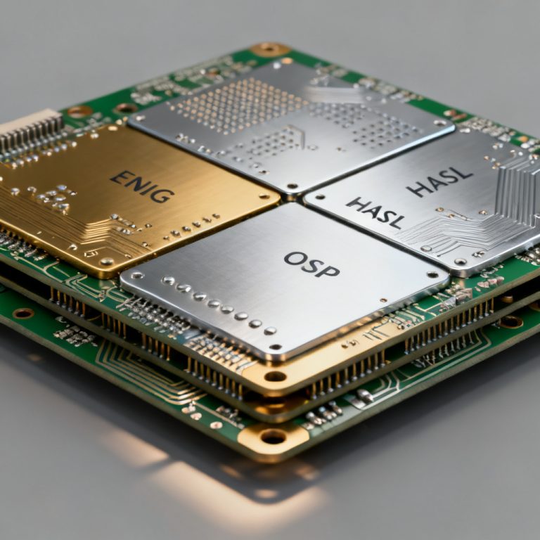
After etching and resist stripping, the inner layer copper must be treated to promote adhesion to the prepreg during lamination. Traditional black oxide forms a black cupric oxide (CuO) coating but has disadvantages like pink ring and potential corrosion. Alternative processes include brown oxide (cuprous oxide, Cu₂O), reduced oxide (chemical reduction to metallic copper with a rough surface, eliminating pink ring), and direct bonding films (e.g., ABF film) for HDI boards.
3.3 Inspection and Testing Before Lamination
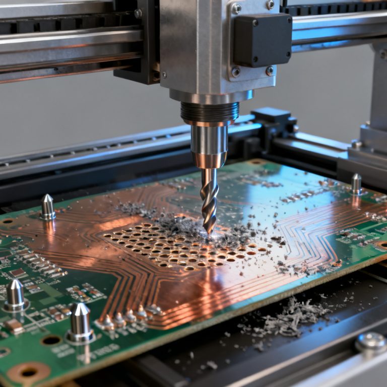
Before lamination, inner layers undergo rigorous inspection: automated optical inspection (AOI) for opens, shorts, pinholes, and copper slivers; electrical testing (flying probe or fixture-based) for complex boards; and micro-sectioning to verify etch quality and resist adhesion.
3.4 Environmental and Safety Considerations
Etchant regeneration (closed-loop cupric chloride systems), wastewater treatment for copper and organic compounds, photoresist recycling (not widespread), and proper ventilation for fumes (HCl, chlorine, ammonia) are essential.
Conclusion: Achieving Perfection in Inner Layer Fabrication
Inner layer imaging and etching for multilayer PCBs are the most critical processes in multilayer PCB manufacturing. They determine the electrical performance, reliability, and yield of the final product. By mastering the materials (dry film photoresist, copper-clad laminate), the processes (lamination, exposure, development, etching), and the quality control measures (AOI, registration, surface treatment), manufacturers can produce boards with fine lines, tight tolerances, and high layer counts. For design engineers, understanding these processes is equally important. Specifying appropriate line widths, copper weights, and material choices, while accounting for etch compensation and registration tolerances, will ensure that your design is manufacturable and reliable.
At [Your Company Name], we leverage state-of-the-art LDI systems, closed-loop cupric chloride etching, and strict IPC Class 3 inspection protocols to deliver multilayer PCBs that meet the highest industry standards. Contact us for your next high-complexity project.
FAQ: Inner Layer Imaging and Etching for Multilayer PCBs
What is inner layer imaging in PCB manufacturing?
Inner layer imaging is the process of transferring circuit patterns onto copper-clad laminate using photoresist and UV light, enabling fine-line accuracy for inner layer imaging and etching for multilayer PCBs.
Why is inner layer etching critical for multilayer PCBs?
Inner layer etching precisely removes unwanted copper, defining the circuit traces that carry signals and power. Proper etching prevents shorts, opens, and impedance issues in inner layer imaging and etching for multilayer PCBs.
What are common defects in inner layer etching?
Common defects include undercut, incomplete etching, and resist lifting. Solutions involve adjusting etch parameters, improving cleaning, and using LDI for better registration in inner layer imaging and etching for multilayer PCBs.
How to ensure layer alignment in multilayer PCBs?
Use tooling holes, X-ray registration, and material compensation factors. LDI systems offer real-time scaling for precise registration in inner layer imaging and etching for multilayer PCBs.