Skip to content

PCB Types

  • Home
PCB Types
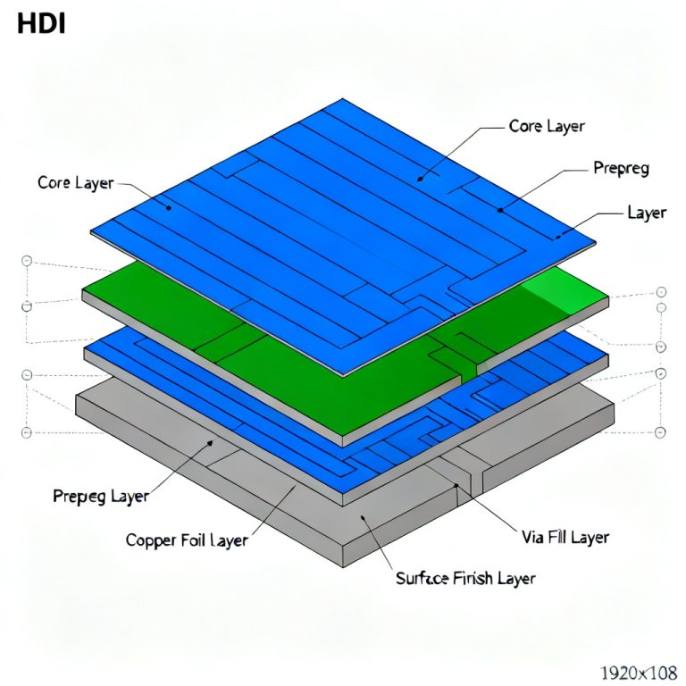
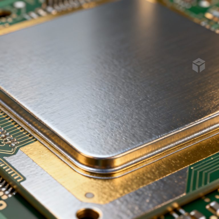
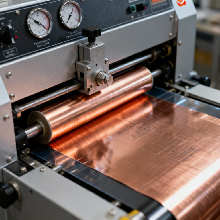
  • HDI Manufacturing Microvia Fill and Lay up engineering diagram showing sequential lamination stackup design with copper-filled blind microvias and ultra-thin dielectrics
    PCB Manufacturing Processes | HDI Manufacturing

    HDI Manufacturing Microvia Fill and Lay up

    Byroot 2026-06-112026-06-11

    HDI Manufacturing is essential for modern compact electronics, enabling high‑density interconnects through precise microvia formation, via filling, and layer lay‑up. This guide:”HDI Manufacturing Microvia Fill and Lay up” covers every critical process for reliable HDI PCB production. HDI Manufacturing: Microvia Technology, Types, and Reliability What Is a Microvia in HDI Manufacturing? A microvia is a…
    Read More HDI Manufacturing Microvia Fill and Lay upContinue

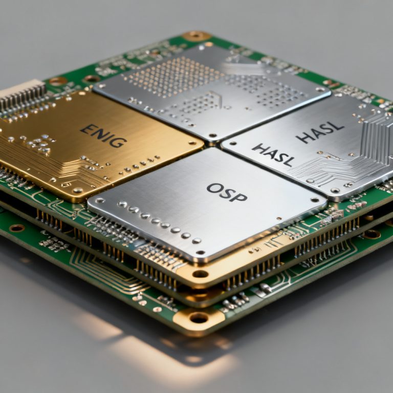
  • PCB Surface Finish Materials ENIG HASL OSP Immersion inspection comparing electroless nickel gold plating flatness and hot air solder leveling pad thickness.
    PCB Materials & Substrates | Surface Finish Materials

    PCB Surface Finish Materials ENIG HASL OSP Immersion

    Byroot 2026-06-112026-06-11

    PCB Surface Finish Materials – ENIG, HASL, OSP, Immersion: A Comprehensive Guide for B2B Buyers Introduction: Why Surface Finish Matters in PCB Manufacturing In the world of printed circuit board (PCB) production, the surface finish is a critical factor that determines solderability, reliability, and long-term performance of your electronic assemblies. Whether you are designing high-frequency…

    Read More PCB Surface Finish Materials ENIG HASL OSP ImmersionContinue

  • Inner Layer Imaging and Etching for Multilayer PCBs line running automated laser direct imaging LDI and chemical spray copper etching.
    PCB Manufacturing Processes | Inner Layer Etching

    Inner Layer Imaging and Etching for Multilayer PCBs

    Byroot 2026-06-102026-06-10

    In the world of advanced electronics, inner layer imaging and etching for multilayer PCBs define the quality, reliability, and functionality of high-density devices. Unlike simple double-sided boards, multilayer PCBs consist of several layers of conductive copper and insulating dielectric material, laminated together under heat and pressure. The quality, reliability, and functionality of these boards hinge…

    Read More Inner Layer Imaging and Etching for Multilayer PCBsContinue

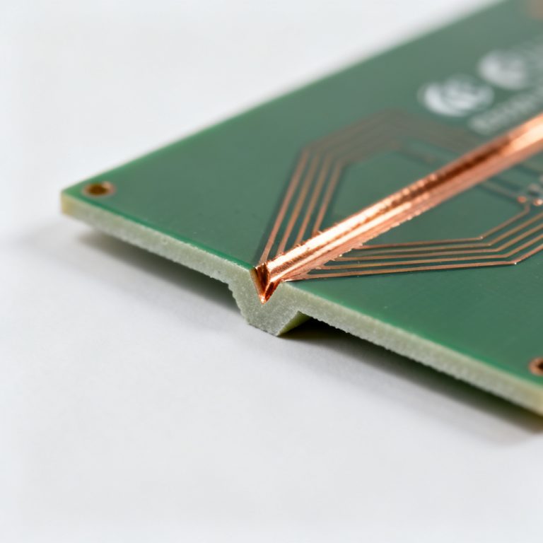
  • PCB Routing and Profiling VS coring Tab Routing setup displaying CNC routing bits, break-away tabs layout, and V-groove depth comparison on a production panel.
    PCB Manufacturing Processes | Routing & Profiling

    PCB Routing and Profiling VS coring Tab Routing

    Byroot 2026-06-102026-06-10

    PCB Routing and Profiling VS coring Tab Routing are the final mechanical steps in printed circuit board fabrication, where individual boards are separated from a larger production panel. This process is critical because it directly impacts board edge quality, component integrity, and assembly yield. Two primary methods dominate the industry: V‑Scoring and Tab Routing (also…

    Read More PCB Routing and Profiling VS coring Tab RoutingContinue

  • Advanced multi-layer board surface finish inspection featuring ENIG flat pad planarity and Immersion Silver circuit trace details according to IPC standards.
    PCB Manufacturing Processes | PCB Surface Finish Guide

    PCB Surface Finish Guide ENIG HASL OSP Immersion Silver Tin

    Byroot 2026-06-092026-06-09

    This post “PCB Surface Finish Guide ENIG HASL OSP Immersion Silver Tin”provides a comprehensive comparison of ENIG, HASL, OSP, Immersion Silver, and Immersion Tin. Whether you are designing high-frequency RF boards, medical devices, or automotive electronics, choosing the right PCB surface finish is critical for reliability and cost. This guide consolidates expertise from leading manufacturers…

    Read More PCB Surface Finish Guide ENIG HASL OSP Immersion Silver TinContinue

  • FR 4 Materials Standard High Tg Halogen Free
    PCB Materials & Substrates | Ultimate Guide to PCB Materials

    FR 4 Materials Standard High Tg Halogen Free

    Byroot 2026-06-042026-06-05

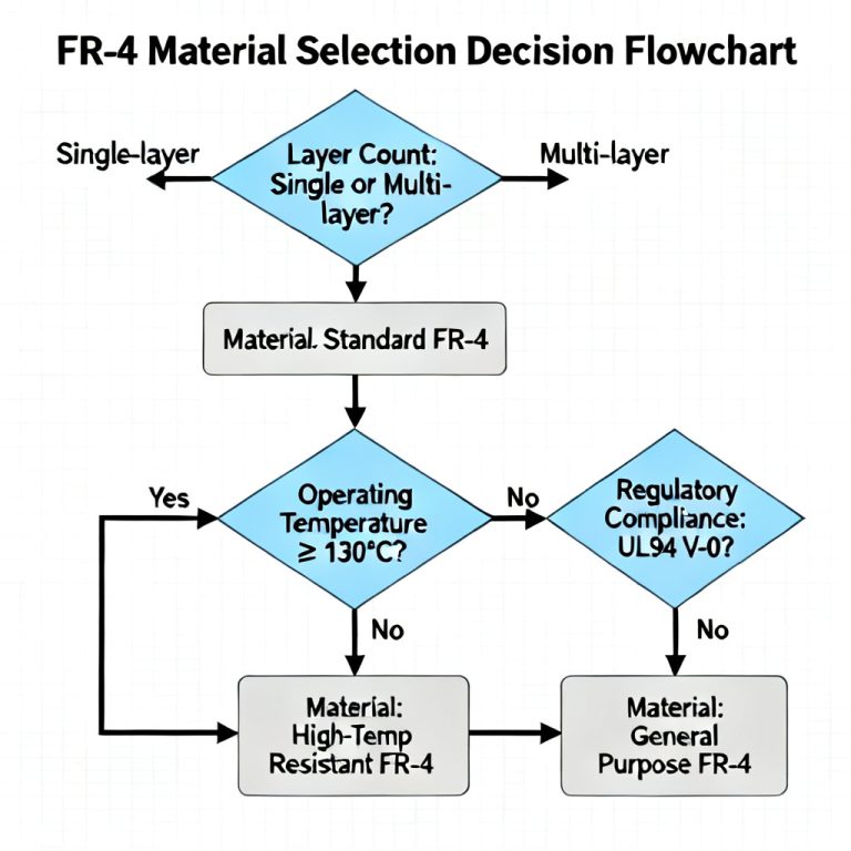
    FR‑4 Materials – Standard, High‑Tg, Halogen‑Free: The Complete Guide for PCB Design and Manufacturing Introduction: Why FR‑4 Matters in PCB Production FR‑4 (Flame Retardant 4) is the most widely used substrate material in the printed circuit board (PCB) industry, accounting for over 90% of all rigid PCBs manufactured globally. It is a glass-reinforced epoxy laminate…

    Read More FR 4 Materials Standard High Tg Halogen FreeContinue

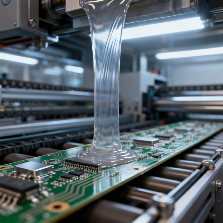
  • Solder Mask Application LPI Spray and Curtain manufacturing line showing automated curtain coating head dispensing liquid epoxy resin on a moving PCB panel
    PCB Manufacturing Processes | Solder Mask Application

    Solder Mask Application LPI Spray and Curtain

    Byroot 2026-05-272026-06-05

    Solder mask application is a critical process in PCB manufacturing that determines board reliability, resolution, and cost. This guide Solder Mask Application LPI Spray and Curtaincovers three primary solder mask application methods—Liquid Photoimageable (LPI), Spray, and Curtain Coating—to help B2B buyers make informed decisions for custom PCB production and export. 1. Liquid Photoimageable (LPI) Solder…

    Read More Solder Mask Application LPI Spray and CurtainContinue

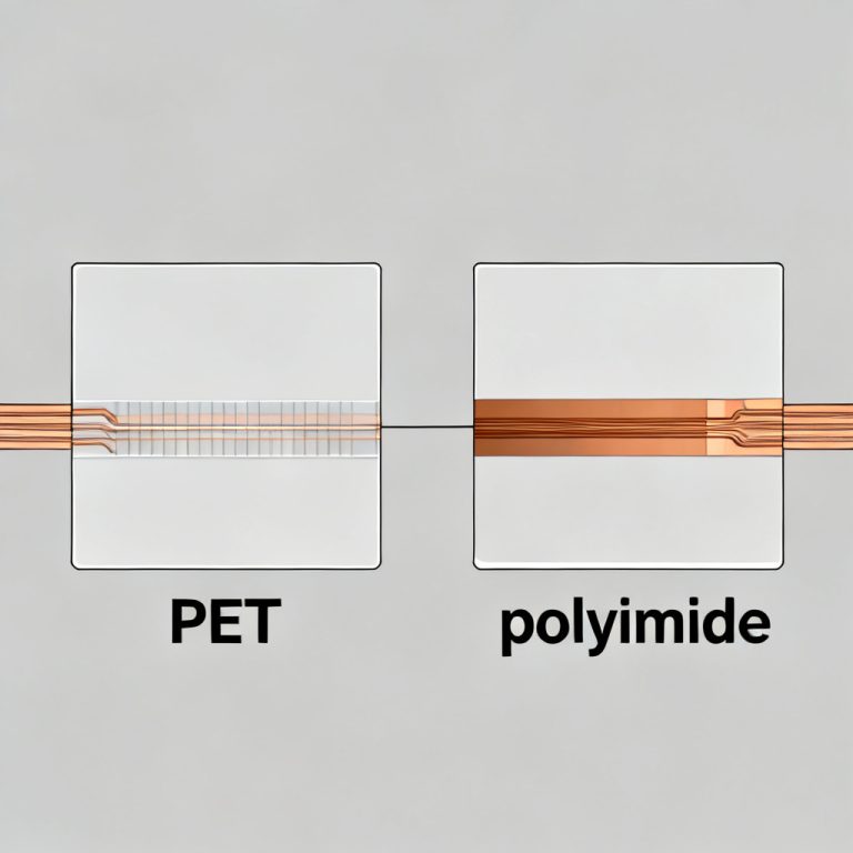
  • Flexible PCB Materials Polyimide PET Coverlay
    PCB Materials & Substrates | Flexible Materials

    Flexible PCB Materials Polyimide PET Coverlay

    Byroot 2026-05-272026-06-03

    Flexible PCB Materials Polyimide PET Coverlay define the performance and reliability of modern flex circuits. In this comprehensive guide, we explore every aspect of these critical substrates and protective layers, helping engineers and buyers make informed decisions for dynamic, high-temperature, or cost-sensitive applications. Understanding Flexible PCB Materials: Polyimide, PET, and Coverlay Polyimide (PI): The Gold…

    Read More Flexible PCB Materials Polyimide PET CoverlayContinue

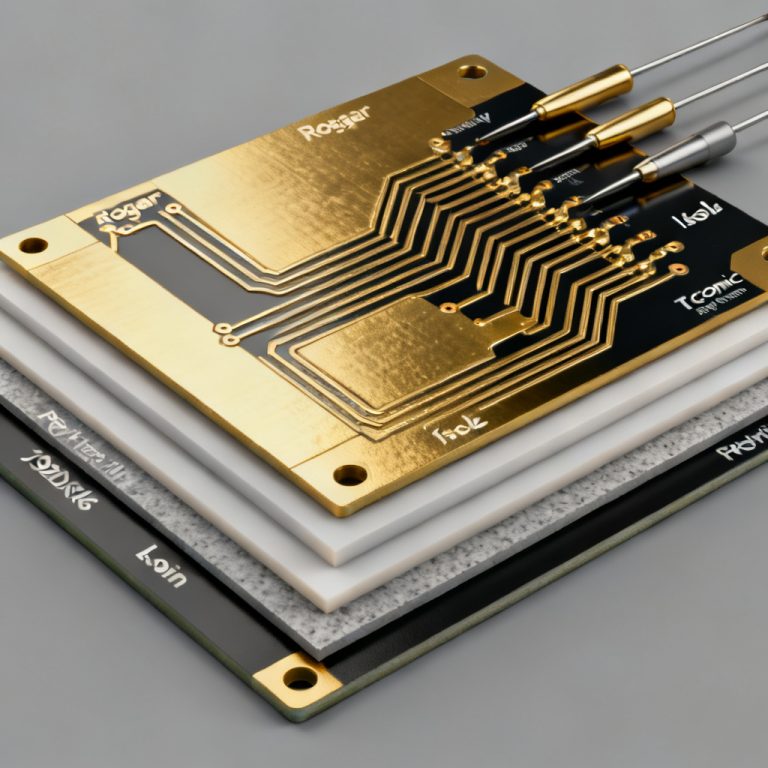
  • High Frequency Materials Rogers PTFE Isola Taconic
    PCB Materials & Substrates | High-Frequency Materials

    High Frequency Materials Rogers PTFE Isola Taconic

    Byroot 2026-05-272026-05-27

    In high‑frequency PCB design, selecting the right High Frequency Materials Rogers PTFE Isola Taconic is critical for signal integrity and low loss. Standard FR‑4 fails above a few hundred MHz, making specialized laminates mandatory for 5G, radar, and aerospace. This guide covers all key parameters, product families, and selection criteria. Why Standard FR‑4 Fails at High…

    Read More High Frequency Materials Rogers PTFE Isola TaconicContinue

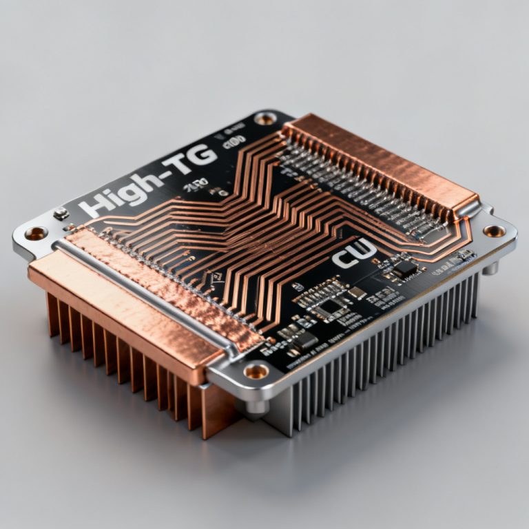
  • High Tg PCB Guide Advantages Materials Applications
    PCB Materials & Substrates | High-Tg PCB Guide

    High Tg PCB Guide Advantages Materials Applications

    Byroot 2026-05-272026-05-27

    This High Tg PCB Guide Advantages Materials Applications explains everything you need to know about glass transition temperature, material selection, and thermal reliability. High‑Tg PCBs are essential for automotive, aerospace, and industrial electronics that demand stable performance under extreme heat. Whether you are designing a power inverter, an engine control unit, or a satellite communication module,…

    Read More High Tg PCB Guide Advantages Materials ApplicationsContinue

Page navigation

Previous PagePrevious 1 … 4 5 6 7 8 … 11 Next PageNext

© 2026 PCB Types Powered by PCBTypes

  • Home