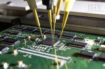
Inspection Methods AOI SPI X ray ICT
In PCB manufacturing, Inspection Methods – AOI, SPI, X‑ray, ICT are the cornerstone of zero‑defect quality assurance. A single defect can cause catastrophic failures in electronics—from consumer devices to aerospace systems. To guarantee reliability, manufacturers rely on these four critical inspection techniques. This guide explores each method’s principles, applications, strengths, and limitations, helping you make informed decisions for your custom PCBs.
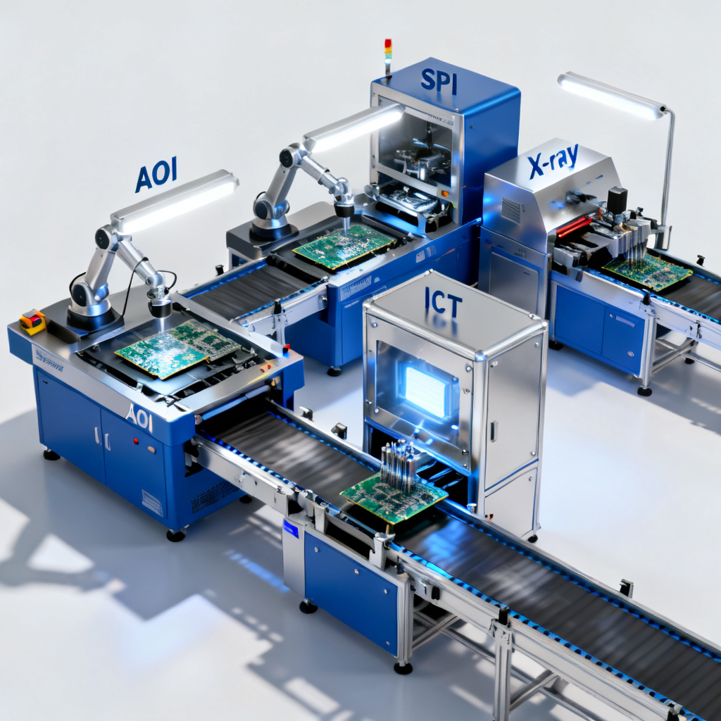
Overview of PCB Inspection Methods: AOI, SPI, X‑ray, ICT
PCB inspection is a multi‑stage process designed to catch defects at every manufacturing step. Each method serves a unique purpose: Inspection Methods – AOI, SPI, X‑ray, ICT detect surface defects, paste errors, hidden voids, and electrical faults respectively. By combining these techniques, manufacturers achieve near‑100% defect detection, minimizing field failures and returns.
Automated Optical Inspection (AOI) – Surface Defect Detection
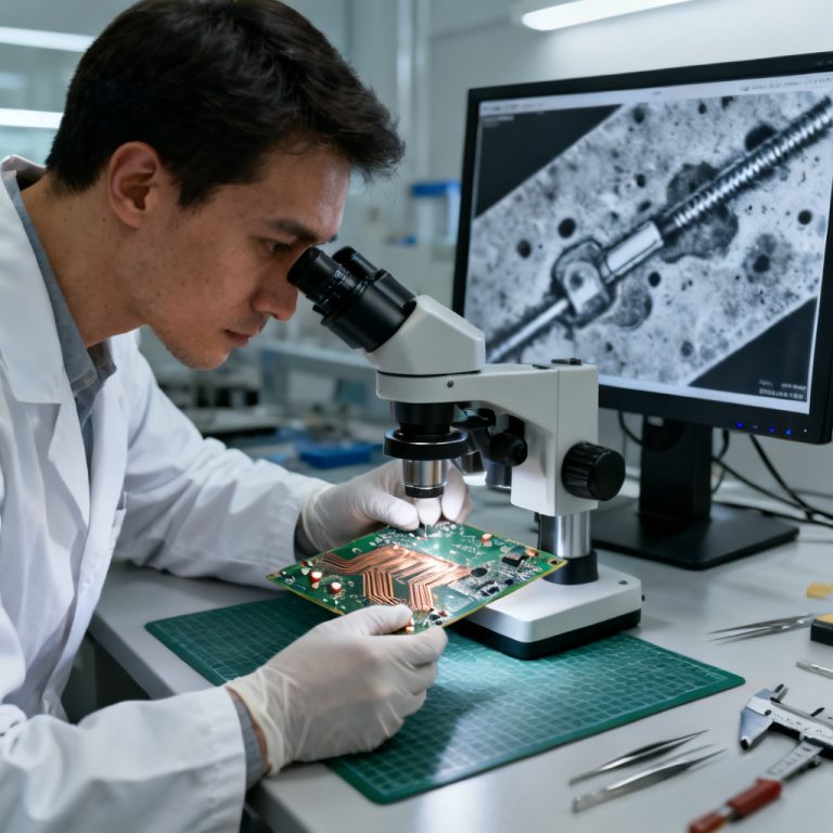
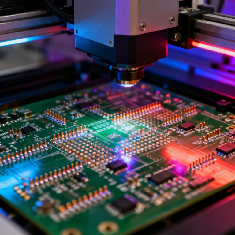
Automated Optical Inspection uses high‑resolution cameras and advanced image processing algorithms to inspect PCBs for surface defects. It is typically employed after solder reflow to verify component placement, solder joint quality, and board cleanliness. A camera captures multiple images from different angles, comparing them against a golden board or CAD data. Algorithms detect anomalies such as missing components, tombstoning, insufficient solder, bridges, or misalignment.
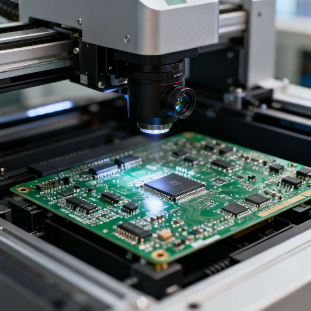
Advantages of AOI include speed (hundreds of boards per hour), repeatability, non‑contact testing, and cost‑effectiveness by reducing manual visual inspection labor. Limitations include surface‑only detection (cannot see internal defects like BGA voids), false calls requiring human review, and sensitivity to lighting conditions. AOI is ideal for high‑volume SMT assembly lines where speed and consistency are critical, and for post‑reflow inspection in prototypes and medium‑volume runs.
Solder Paste Inspection (SPI) – Paste Volume and Alignment
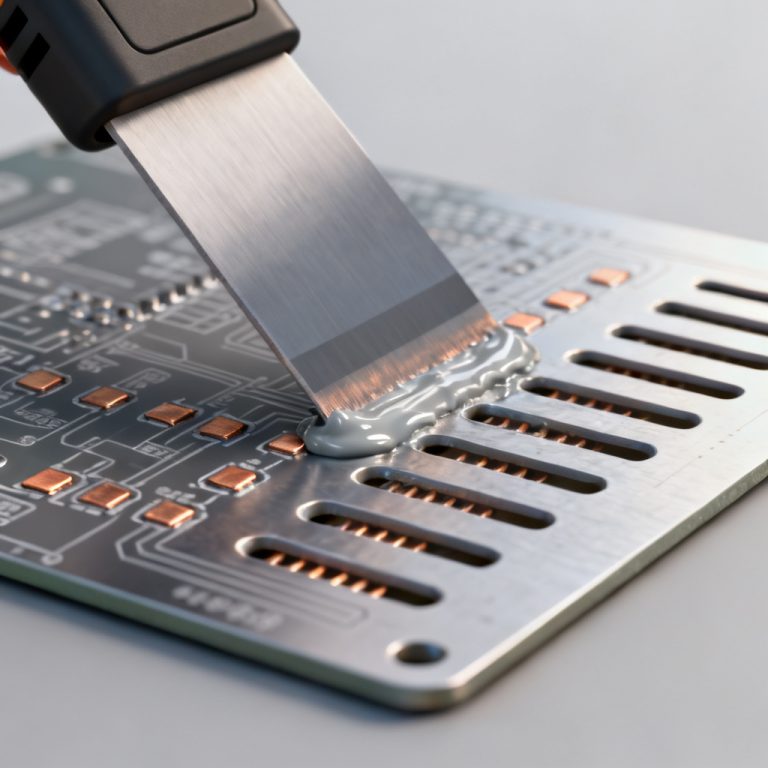
Solder Paste Inspection occurs before component placement, measuring the volume, area, height, and alignment of solder paste deposits on PCB pads. SPI is crucial because 60–70% of soldering defects originate from poor paste deposition. A 3D laser scanner or structured light projects a pattern onto the paste; the system calculates paste volume by analyzing height and area data, comparing results to predefined tolerances (e.g., ±10% of target volume).
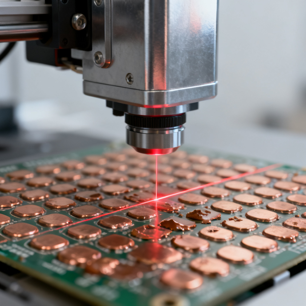
Advantages of SPI include early defect detection (catches insufficient or excessive paste before components are placed), process control (provides statistical data to optimize stencil printing parameters), and reduced rework by preventing downstream defects like opens or shorts. Limitations include no component verification, slower speed than 2D AOI for paste inspection (though modern 3D systems are comparable), and higher initial investment than 2D systems. SPI is mandatory for fine‑pitch components (e.g., 0.4mm BGA) and high‑reliability applications (automotive, medical), and is also used for process validation during new product introduction.
X‑ray Inspection – Internal Defect Detection
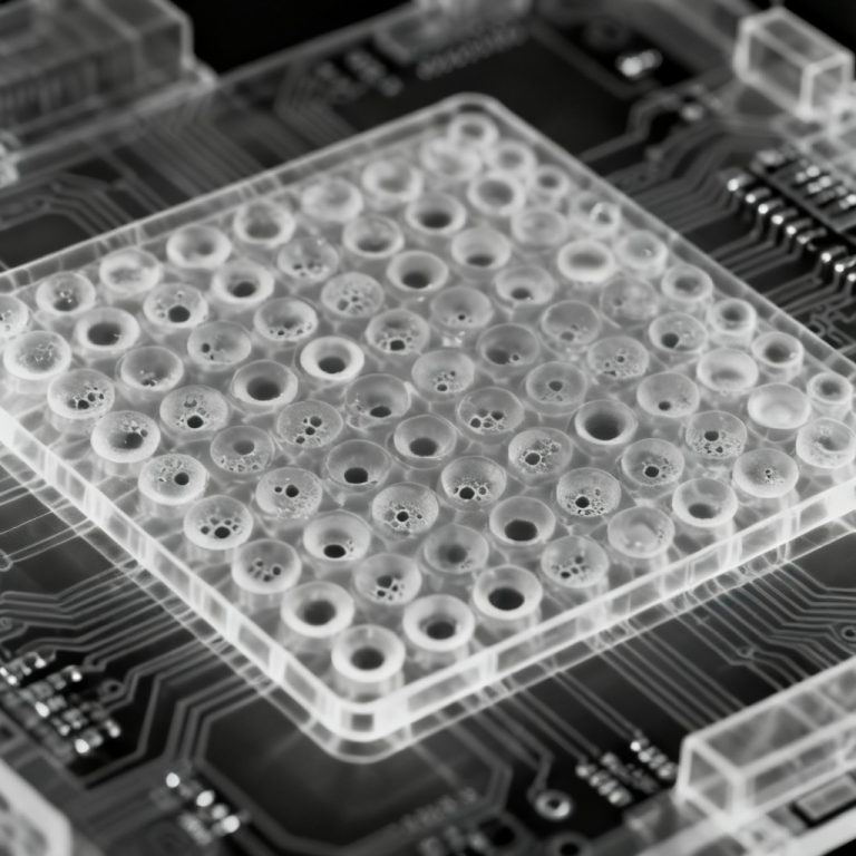
X‑ray inspection uses penetrating radiation to create images of a PCB’s internal structures. It is essential for inspecting hidden solder joints in BGA, QFN, and other area‑array packages, as well as detecting voids, cracks, and misalignments. An X‑ray source emits radiation through the PCB; a detector captures the transmitted image, revealing density variations. Software analyzes the image for defects like voids (gas pockets in solder joints), bridging (unwanted connections), missing balls (incomplete BGA connections), and misalignment (shifted components).
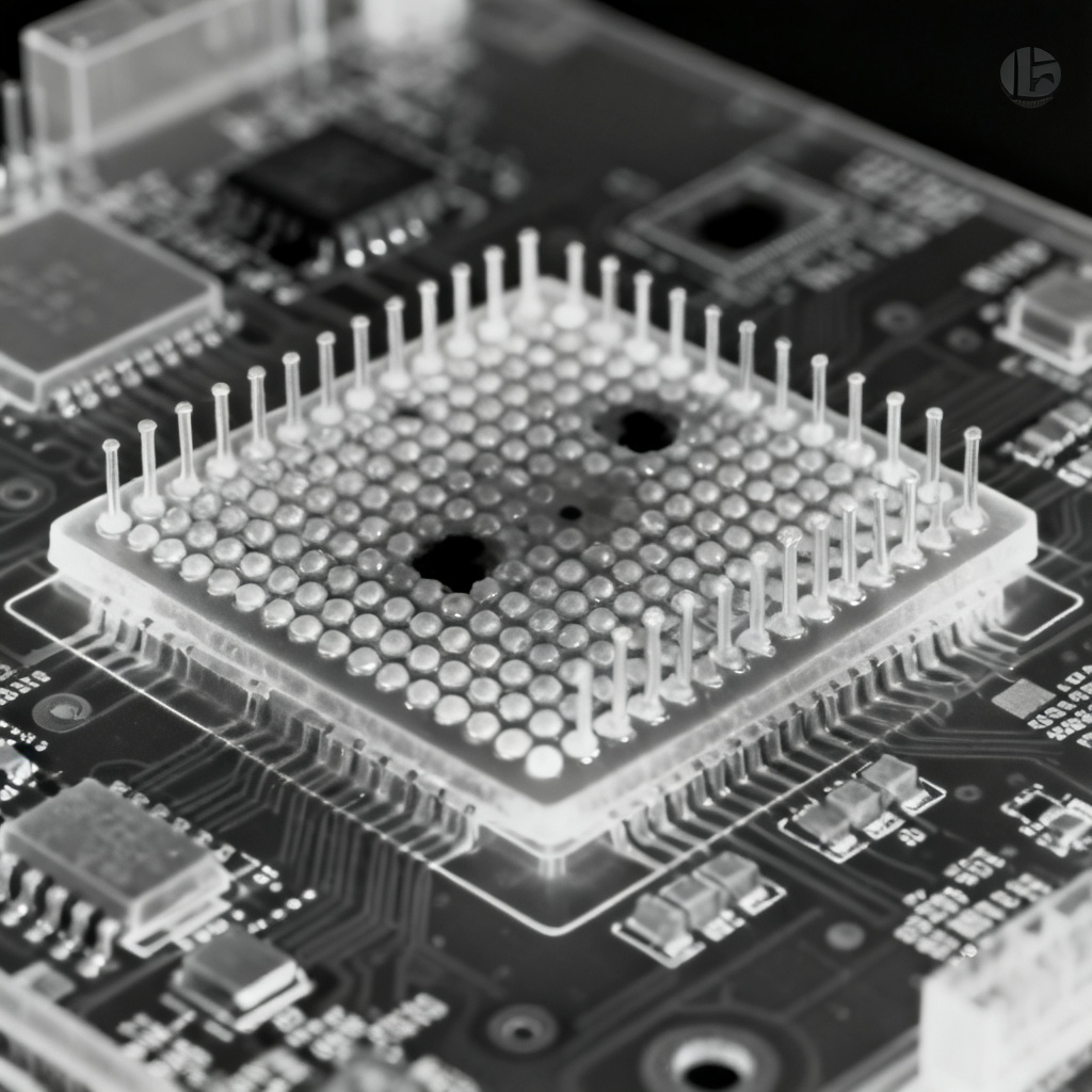
Types of X‑ray systems include 2D X‑ray (fast, low‑cost, limited to planar defects) and 3D CT (Computed Tomography) which generates cross‑sectional images for depth analysis, ideal for complex assemblies. Advantages include internal defect detection unmatched for hidden joints, non‑destructive testing, and quantitative void analysis per IPC‑7095 standards. Limitations include high equipment and maintenance costs, safety requirements (shielding and operator training), and need for skilled operators to distinguish defects from normal variations. X‑ray is essential for BGA, QFN, and PoP (Package on Package) assemblies, and used in aerospace, medical, and military applications where reliability is paramount.
In‑Circuit Testing (ICT) – Electrical Verification
In‑Circuit Testing (ICT) is an electrical test that verifies the functionality of individual components on a populated PCB. It uses a bed‑of‑nails fixture to contact test points and measure resistance, capacitance, inductance, and diode drops. The tester applies voltages/currents and measures responses, testing for opens and shorts, component values (resistors, capacitors, inductors), polarity (diode and capacitor orientation), and power‑up tests (ensuring voltage regulators output correct values).
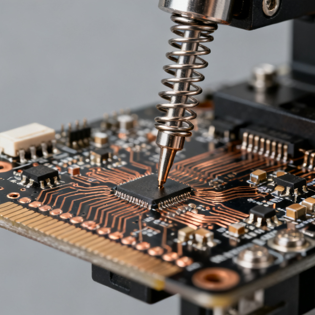
Advantages of ICT include high fault coverage (catches 90–95% of assembly defects), rapid diagnosis (pinpoints the exact faulty component), and repeatability through automation. Limitations include fixture cost (expensive for low‑volume or complex boards), access constraints (requires test points; not suitable for dense designs), and no functional test (does not verify board‑level performance like timing or signal integrity). ICT is best for high‑volume production where fixture cost is amortized, and for boards with known high failure rates. For prototypes, flying probe testers (a fixture‑less alternative) are preferred.
Comparison Table: Inspection Methods – AOI vs. SPI vs. X‑ray vs. ICT
| Inspection Method | Stage | Detects | Speed | Cost | Best For |
|---|---|---|---|---|---|
| AOI | Post‑reflow | Surface defects (missing parts, bridges, misalignment) | High | Medium | High‑volume SMT |
| SPI | Pre‑placement | Solder paste volume, height, alignment | Medium | Medium‑High | Fine‑pitch & high‑reliability |
| X‑ray | Post‑reflow | Internal defects (voids, BGA balls, misalignment) | Medium | High | BGA, QFN, hidden joints |
| ICT | Post‑assembly | Electrical opens, shorts, component values | High | High (fixture) | High‑volume, known defects |
How to Choose the Right Inspection Method for Your PCB
Selecting the right Inspection Methods – AOI, SPI, X‑ray, ICT depends on your PCB’s complexity, volume, and reliability requirements. For simple boards with visible components, AOI alone may suffice. For fine‑pitch or high‑reliability designs, combine SPI + AOI + X‑ray. For mission‑critical applications (aerospace, medical), add ICT for electrical verification. For prototypes or low volume, use flying probe ICT (fixture‑less) instead of bed‑of‑nails.
Integration and Best Practices for Inspection Methods
Modern PCB manufacturers integrate these methods into a closed‑loop quality system. SPI feeds paste‑printing data back to the stencil printer for real‑time adjustment. AOI flags reflow defects, which are analyzed to optimize reflow profiles. X‑ray validates BGA quality, especially for lead‑free solders prone to voids. ICT provides final electrical sign‑off before functional testing. Best practices include calibrating all systems regularly (e.g., daily for AOI, weekly for X‑ray), using statistical process control (SPC) to monitor defect trends, training operators to distinguish true defects from false calls, and documenting inspection criteria per IPC‑610 (acceptability) and IPC‑7095 (BGA voids).
Common Myths and Misconceptions About PCB Inspection
Myth: AOI can replace X‑ray for BGA inspection. Fact: AOI only sees surface; X‑ray is mandatory for hidden joints. Myth: SPI is unnecessary if AOI is used. Fact: SPI prevents defects at the source; AOI catches them later—both are complementary. Myth: ICT is obsolete due to flying probe testers. Fact: ICT remains faster and more comprehensive for high‑volume runs.
Future Trends in PCB Inspection Methods
AI‑powered defect classification reduces false calls and speeds up review. Inline X‑ray is integrated into SMT lines for real‑time feedback. Digital twins simulate inspection processes for predictive quality. IoT‑enabled testers share real‑time data with cloud‑based analytics.
Frequently Asked Questions About Inspection Methods – AOI, SPI, X‑ray, ICT
Q: Can AOI detect all defects?
A: No. AOI misses internal defects like BGA voids. It should be used with X‑ray for complete coverage.
Q: Is SPI necessary for all PCB designs?
A: Not mandatory, but highly recommended for fine‑pitch components (<0.5mm pitch) and high‑reliability applications.
Q: How much does ICT fixture cost?
A: Typically $1,000–$5,000 per fixture, depending on board complexity and pin count.
Q: What is the void acceptance limit per IPC‑7095?
A: For BGA, voids should be <25% of the ball area for most applications; <15% for high‑reliability.
Conclusion: Master Inspection Methods for Zero‑Defect PCBs
Mastering Inspection Methods – AOI, SPI, X‑ray, ICT is essential for delivering zero‑defect boards. Each technique fills a unique role: SPI prevents paste defects, AOI catches surface issues, X‑ray reveals hidden flaws, and ICT ensures electrical integrity. By combining them strategically, you can achieve the highest quality standards for your custom PCBs. Ready to ensure your PCBs pass every inspection? Contact us today to discuss your project requirements and get a free quote for our comprehensive inspection services.