PCB Testing Guide Flying Probe ICT AOI X ray Microsection
This comprehensive PCB Testing Guide Flying Probe ICT AOI X ray Microsection methods for reliable production. Engineers and procurement managers rely on this guide to choose the right test for their PCB manufacturing needs.
In the competitive world of B2B PCB manufacturing, quality is not just a promise—it is a verifiable, data-driven process. For engineers, procurement managers, and quality assurance teams, understanding the full spectrum of PCB testing methods is critical to ensuring reliability, reducing field failures, and meeting stringent industry standards (IPC-A-600, IPC-6012, etc.). This comprehensive guide covers the five most essential testing techniques: Flying Probe, In-Circuit Test (ICT), Automated Optical Inspection (AOI), X‑ray Inspection, and Microsection Analysis. Each method serves a distinct purpose, from detecting soldering defects to verifying internal layer integrity. By the end of this guide, you will know exactly which test to specify for your prototype, low-volume, or high-volume production runs.
Flying Probe Test: Flexible PCB Testing for Prototypes
What Is Flying Probe Test?
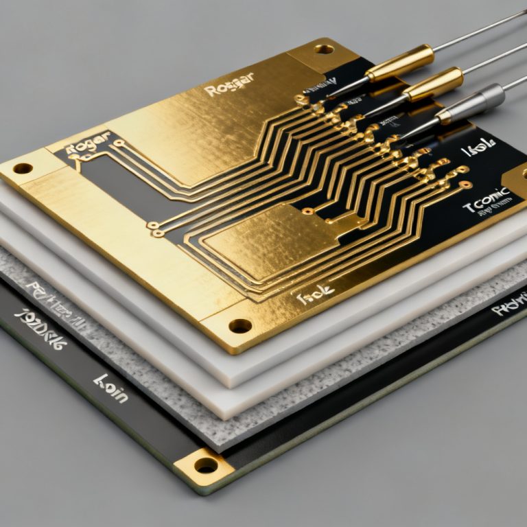
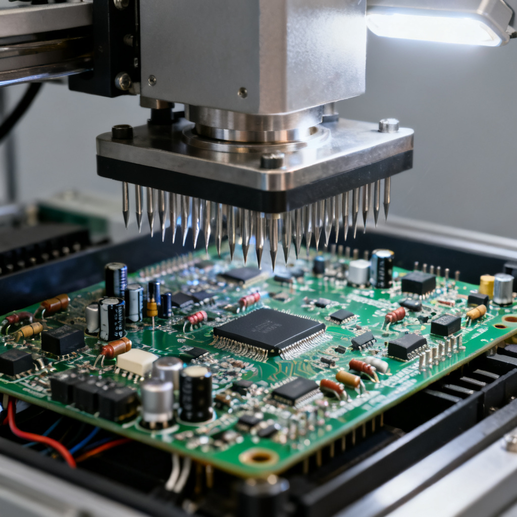
Flying Probe testing is a non‑powered, fixture‑less electrical test that uses two or more independently moving probes to contact test points on a bare PCB. It is the most flexible and cost‑effective method for prototypes and small‑to‑medium volume production.
How Flying Probe Test Works
Setup: No custom test fixture (bed‑of‑nails) is required. The machine uses a program generated from the CAD design files (Gerber, ODB++, or IPC‑2581) to map net connectivity.
Process: Probes move at high speed to sequential test points. Each probe measures continuity (resistance) and isolation (capacitance or resistance between nets). Typical test parameters:
- Continuity: Checks for open circuits (target resistance < 10 Ω, often < 1 Ω for critical nets).
- Isolation: Checks for shorts (target resistance > 10 MΩ, often > 100 MΩ).
- Component Verification: For loaded boards, probes can also measure passive components (resistors, capacitors, diodes) by applying a small voltage and measuring the response.
- Speed: Modern flying probe machines can test 500–1,500 points per hour, depending on probe count (typically 4–8 probes) and board complexity.
Key Advantages of Flying Probe Test
- No Fixture Cost: Ideal for prototypes, low‑volume runs (1–500 boards), and frequent design changes.
- High Accuracy: Probes can reach fine‑pitch components (down to 0.3 mm pitch) and small test points (0.1 mm diameter).
- Flexible Programming: Quick turnaround from CAD data; no mechanical fixture delays.
- Detectable Defects: Opens, shorts, incorrect component values, missing components, and reverse polarity (diodes, capacitors).
Limitations of Flying Probe Test
- Speed: Slower than ICT for high‑volume production (e.g., 1,000+ boards per day).
- Not for Functional Testing: Cannot test power‑on behavior, firmware, or complex analog circuits.
- Probe Wear: Contact probes have limited lifespan (typically 500,000–1 million cycles) and require periodic replacement.
- Limited Coverage: Cannot test components that are shielded or hidden under other components (e.g., BGA balls under the package).
When to Use Flying Probe Test
- Prototyping and NPI (New Product Introduction): When design is still evolving and fixture cost is unjustified.
- Low‑Volume Production: 1–500 boards per batch.
- High‑Mix, Low‑Volume (HMLV) Environments: Many different board types with small quantities.
- Quick Turnaround: When lead time is critical.
In‑Circuit Test (ICT): High‑Speed PCB Testing for Volume
What Is In‑Circuit Test?
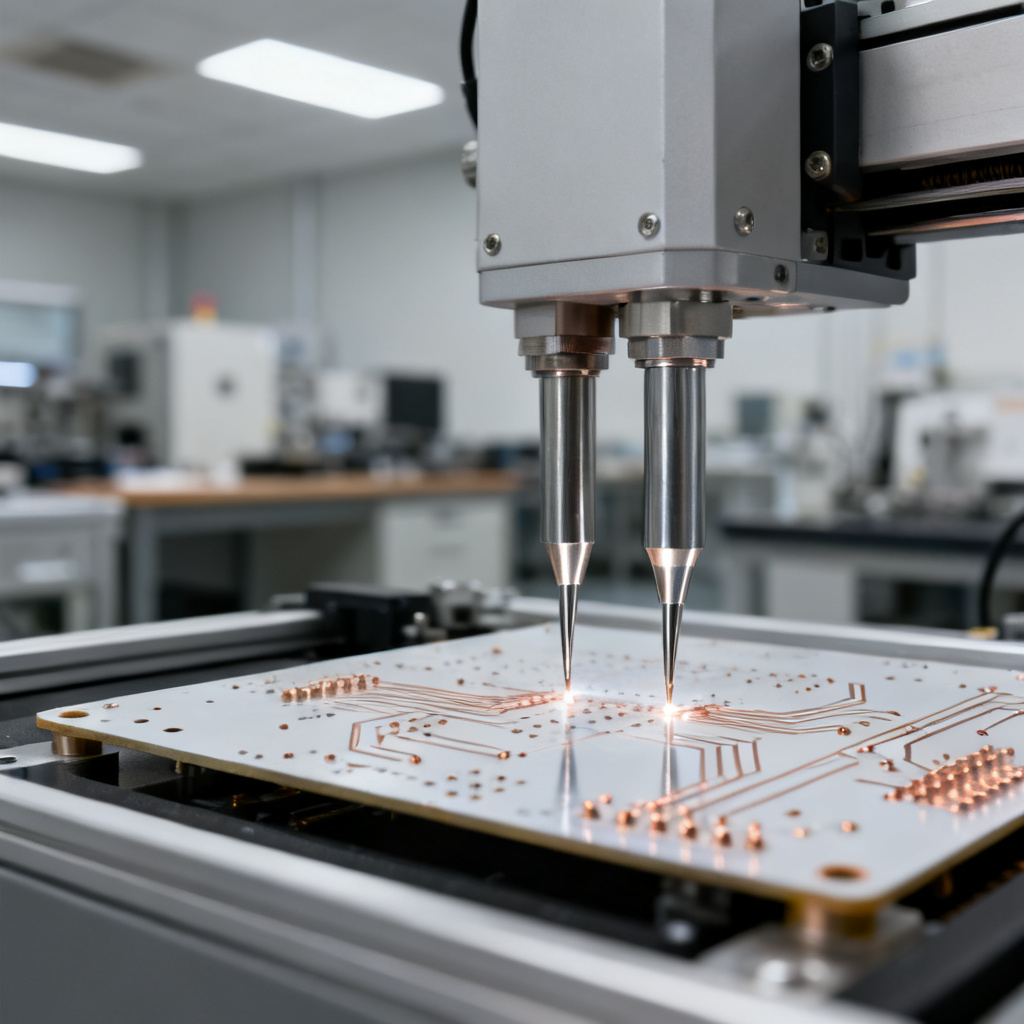
ICT is a high‑speed, fixture‑based electrical test that uses a bed‑of‑nails (pogo pins) to simultaneously contact hundreds or thousands of test points on a loaded PCB. It is the gold standard for high‑volume production testing.
How In‑Circuit Test Works
Setup: A custom test fixture is built with spring‑loaded pogo pins aligned to every test point on the board. The fixture is mounted on a vacuum, pneumatic, or mechanical press.
Process: The board is pressed onto the pins. The tester applies voltage/current from a power supply and measures:
- Analog Measurements: Resistance, capacitance, inductance, diode drop, transistor gain, etc.
- Digital Measurements: Logic levels, open collectors, and basic IC connectivity.
- Component Identification: Reads resistor/capacitor values, checks for missing or wrong parts.
- Speed: A typical ICT can test a complex board in 30–90 seconds (including fixture clamping and release). This translates to 500–1,500 boards per shift per machine.
Key Advantages of In‑Circuit Test
- Extreme Speed: Best for high‑volume production (10,000+ boards per month).
- Comprehensive Component Verification: Can measure exact values of passives, verify polarity, and detect wrong or missing components.
- High Fault Coverage: Detects opens, shorts, wrong components, missing components, reverse polarity, and basic functional errors (e.g., stuck‑at faults in digital ICs).
- Repeatable and Reliable: Fixture‑based system provides consistent contact every time.
Limitations of In‑Circuit Test
- High Fixture Cost: A custom bed‑of‑nails fixture can cost $2,000–$10,000+ depending on complexity. This is amortized only over large volumes.
- Long Lead Time: Fixture design and fabrication takes 2–4 weeks.
- Physical Access Required: Every test point must be accessible on the bottom side of the board (or via edge connectors). Fine‑pitch components (< 0.5 mm pitch) may be difficult to contact.
- Not for Bare Boards: ICT is typically used on assembled (loaded) PCBs. Bare board testing is better suited to flying probe or dedicated bare board testers.
- Component Damage Risk: High‑pressure pins can damage delicate components (e.g., ceramic capacitors) if not properly designed.
When to Use In‑Circuit Test
- High‑Volume Production: 5,000+ boards per batch.
- Mature Designs: No frequent changes that would require a new fixture.
- Complex Boards with Many Test Points: When flying probe speed is insufficient.
- Cost‑Effective Only When Volume Justifies Fixture Investment.
Automated Optical Inspection (AOI) for Surface Defect Detection
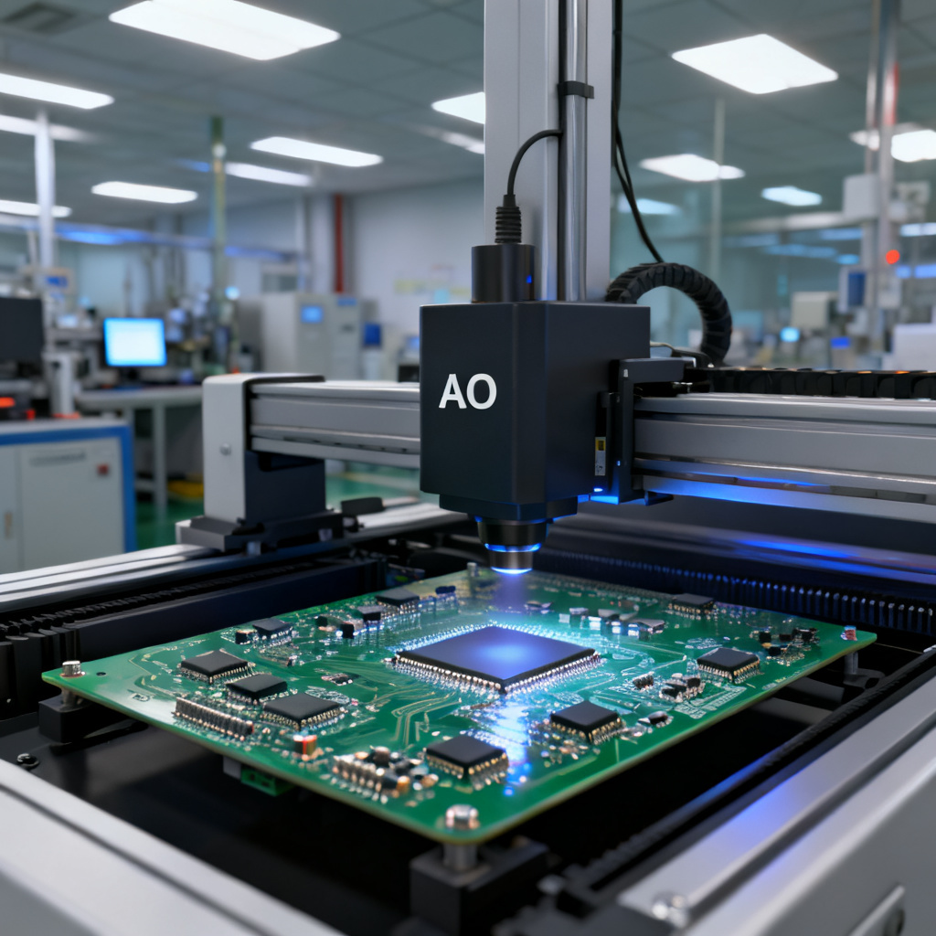
What Is Automated Optical Inspection?
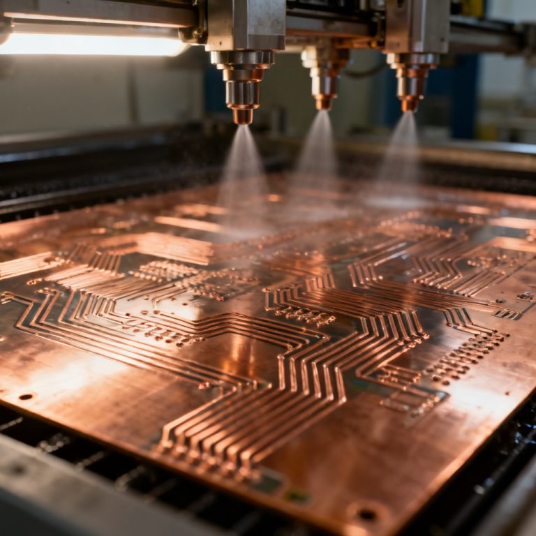
AOI uses high‑resolution cameras and image processing algorithms to visually inspect the PCB assembly for defects. It is typically applied after solder paste printing, after component placement, and after reflow soldering.
How AOI Works
Setup: The board is passed under a line‑scan or area‑scan camera system. The system compares the live image against a golden reference (from CAD data or a known‑good board).
Inspection Parameters:
- Solder Paste: Volume, height, area, and alignment.
- Component Presence/Absence: Missing, wrong, rotated, or tombstoned components.
- Solder Joint Quality: Insufficient/excess solder, bridges, lifted leads, poor wetting.
- Polarity/Alignment: Correct orientation of diodes, capacitors, ICs.
- Speed: Modern 3D AOI systems can inspect a board in 15–60 seconds, depending on complexity.
Key Advantages of AOI
- Non‑Contact: No physical stress on components.
- High Speed: Can be integrated inline with the SMT line for real‑time feedback.
- Detects Visual Defects: Solder bridges, insufficient solder, component misalignment, tombstoning, and missing components.
- 3D Capability: Modern 3D AOI can measure solder paste height and volume, and detect lifted leads or coplanarity issues.
- Data‑Driven: Provides yield statistics and defect maps for process improvement (SPC).
Limitations of AOI
- Cannot Detect Electrical Defects: AOI cannot check for opens, shorts, or component values. It only sees the surface.
- False Positives: Reflection, board warpage, or contamination can trigger false alarms, requiring manual verification.
- Limited Under‑Component Inspection: Cannot see solder joints under BGAs, QFNs, or other hidden packages.
- Programming Time: Creating a golden reference for a new board takes 1–4 hours.
When to Use AOI
- As a Process Control Tool: After solder paste printing to catch paste defects early.
- After Reflow: To catch assembly defects before functional test.
- High‑Volume SMT Lines: Where speed and inline integration are critical.
- Any Board with Fine‑Pitch Components: 0.4 mm pitch and below.
X‑ray Inspection for Hidden Solder Joints and Internal Layers
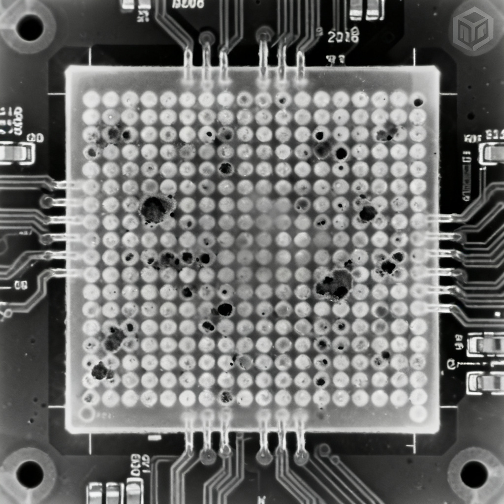
What Is X‑ray Inspection?
X‑ray inspection uses penetrating radiation to create images of internal structures of the PCB assembly. It is the primary method for inspecting hidden solder joints (BGAs, QFNs, connectors) and internal layer defects.
How X‑ray Inspection Works
Setup: The board is placed between an X‑ray source and a detector (flat panel or image intensifier). The X‑rays pass through the board, and the detector captures the attenuation pattern.
Inspection Capabilities:
- BGA Solder Joints: Voids, bridges, insufficient solder, head‑in‑pillow, open balls.
- QFN/QFP: Solder fillet quality, bridging, poor wetting.
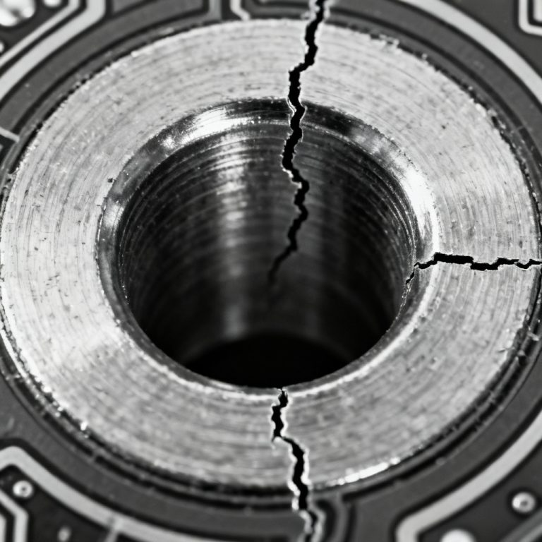
- Through‑Hole Components: Solder fill percentage, barrel cracks, voids.
- Internal Layers (Bare Board): Misalignment, delamination, etch defects, copper nodules, and drill‑to‑copper registration.
- Component Alignment: BGA ball shift, package coplanarity.
- Speed: Manual X‑ray inspection (operator‑driven) takes 2–10 minutes per board. Automated X‑ray inspection (AXI) can inspect a board in 30–90 seconds.
Key Advantages of X‑ray Inspection
- Only Method for Hidden Solder Joints: Essential for BGAs, QFNs, PoP (Package‑on‑Package), and other area‑array packages.
- Internal Layer Analysis: Can detect defects in multilayer PCB construction (e.g., inner layer shorts, voids in prepreg).
- Non‑Destructive: No physical contact or damage to the board.
- Void Measurement: Can quantify void percentage (per IPC‑7095, typically < 25% void area per ball is acceptable).
Limitations of X‑ray Inspection
- Slow for High Volume: Manual X‑ray is time‑consuming. AXI is faster but still slower than AOI.
- Operator‑Dependent: Manual inspection requires skilled operators to interpret images.
- Safety: Requires lead‑lined cabinets and strict safety protocols.
- Cost: X‑ray systems are expensive ($50,000–$200,000+). AXI systems are even costlier.
- Limited Component Value Testing: Cannot measure resistance/capacitance.
When to Use X‑ray Inspection
- Any Board with BGAs, QFNs, or Other Area‑Array Packages: Mandatory for these components.
- High‑Reliability Applications: Aerospace, medical, automotive, military.
- First Article Inspection (FAI): To verify solder joint quality on a new design.
- Failure Analysis: To diagnose field returns or production defects.
- Bare Board Internal Layer Verification: For multilayer boards with fine line/space.
Microsection Analysis for Internal Structure Verification
What Is Microsection Analysis?
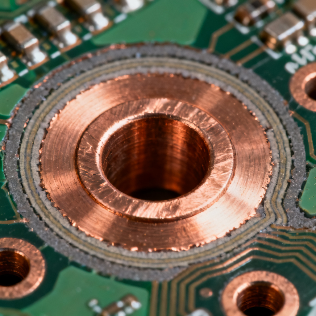
Microsection analysis is a destructive testing method where a cross‑section of the PCB is cut, polished, and examined under a microscope. It is used to verify internal construction quality, plating integrity, and compliance with IPC standards.
How Microsection Analysis Works
Process:
- Sample Preparation: A coupon or a section of the production board is cut using a diamond saw.
- Mounting: The sample is embedded in epoxy resin.
- Grinding and Polishing: The sample is ground with progressively finer abrasives (typically 120–1200 grit) and polished to a mirror finish.
- Etching (Optional): A chemical etch (e.g., ammonium persulfate) may be used to highlight copper grain structure.
- Microscopic Examination: The cross‑section is viewed under an optical microscope (50x–1000x magnification) or SEM.
Measured Parameters:
- Copper Thickness: Outer layer and inner layer copper (target: 1 oz = 35 µm, 2 oz = 70 µm, etc.).
- Plating Thickness: Through‑hole barrel plating (target: 20–25 µm minimum per IPC‑6012).
- Hole Wall Quality: Smoothness, cracks, voids, nodules.
- Dielectric Thickness: Prepreg and core thickness (for impedance control).
- Registration: Drill‑to‑copper alignment (target: ±5 mils or better).
- Inner Layer Distance: Minimum dielectric gap (for voltage breakdown).
- Void Detection: In plating or solder joints (per IPC‑7095).
- Interconnect Defects: Separation between inner layer copper and plated barrel.
Key Advantages of Microsection Analysis
- Most Detailed Internal View: Reveals defects invisible to X‑ray (e.g., plating cracks, inner layer misalignment).
- Quantitative Data: Provides exact measurements for copper, plating, and dielectric thickness.
- IPC Compliance Verification: Essential for IPC‑6012 Class 2/3 certification.
- Failure Analysis: Can pinpoint root cause of field failures (e.g., barrel crack due to thermal stress).
Limitations of Microsection Analysis
- Destructive: The sample is destroyed. Cannot be used on production boards that will be shipped.
- Time‑Consuming: Sample preparation takes 2–4 hours per coupon.
- Sampling Only: Only a small area of the board is analyzed. Defects elsewhere may be missed.
- Skilled Operator Required: Proper grinding/polishing technique is critical to avoid artifacts.
When to Use Microsection Analysis
- First Article Inspection (FAI): To verify that the bare board meets IPC requirements.
- Qualification of New PCB Supplier: To validate their manufacturing capability.
- Periodic Process Control: Every production lot or every 100 boards (per IPC‑6012).
- Failure Analysis: When X‑ray or electrical tests indicate a potential internal defect.
- High‑Reliability Applications: Aerospace, medical, automotive, defense (Class 3).
Comparison Table: Choosing the Right PCB Testing Method
| Test Method | Type | Speed | Cost per Board | Best For | Cannot Detect |
|---|---|---|---|---|---|
| Flying Probe | Electrical (bare or loaded) | Slow (500–1500 pts/hr) | Low (no fixture) | Prototypes, low volume, fine pitch | Hidden joints, internal layers |
| ICT | Electrical (loaded) | Fast (30–90 sec/board) | High (fixture cost) | High volume, component verification | Hidden joints, internal layers |
| AOI | Optical (surface) | Fast (15–60 sec/board) | Medium | Solder paste, component placement, surface defects | Electrical defects, hidden joints |
| X‑ray | Radiographic (internal) | Medium (30–90 sec AXI) | High (equipment cost) | BGA, QFN, internal layer, hidden joints | Component values, electrical function |
| Microsection | Destructive (cross‑section) | Very slow (2–4 hrs) | Very high (per sample) | IPC compliance, plating quality, internal defects | Large‑area coverage, production boards |
Recommended PCB Testing Strategy
For a robust quality assurance program, combine multiple methods:
- Prototype / NPI: Flying Probe (100% electrical test) + AOI (after reflow) + X‑ray (on BGA/QFN areas) + Microsection (on a coupon for IPC verification).
- Low‑Volume Production (1–500 boards): Flying Probe (100%) + AOI (100%) + X‑ray (sample 10–20% of boards) + Microsection (per lot).
- High‑Volume Production (5,000+ boards/month): ICT (100%) + AOI (100%) + X‑ray (sample 5–10% or per IPC requirement) + Microsection (per lot or per IPC‑6012).
- High‑Reliability / Class 3: ICT (100%) + AOI (100%) + X‑ray (100% on BGA/QFN) + Microsection (every lot or every 100 boards).
Frequently Asked Questions About PCB Testing
What is the difference between Flying Probe and ICT in PCB testing?
Flying Probe is a fixture‑less test ideal for prototypes and low volume, while ICT uses a custom bed‑of‑nails fixture for high‑speed, high‑volume production. Both are electrical tests but ICT is faster and more comprehensive for component verification.
Can AOI replace X‑ray inspection for PCB testing?
No. AOI only inspects the surface and cannot see hidden solder joints under BGAs or QFNs. X‑ray inspection is required for those internal connections. For complete PCB testing, combine AOI with X‑ray.
Why is microsection analysis considered the gold standard for IPC compliance?
Microsection analysis provides the most detailed view of internal PCB structures—copper thickness, plating quality, and layer alignment—making it essential for verifying IPC‑6012 Class 2/3 requirements.
How do I choose between Flying Probe and ICT for my PCB testing?
Choose Flying Probe for prototypes, low volume (under 500 boards), or frequent design changes. Choose ICT for high‑volume production (5,000+ boards) where fixture cost is justified by speed and comprehensive coverage.
What defects can X‑ray inspection detect that other methods miss?
X‑ray inspection detects voids, bridges, and insufficient solder in BGA joints, internal layer misalignment, and drill‑to‑copper registration issues—defects invisible to AOI and electrical tests.
Key PCB Testing Terminology
- Bed‑of‑Nails: A custom fixture with spring‑loaded pins used in ICT to contact test points.
- Continuity: Electrical test to verify a continuous path (low resistance) between two points.
- Isolation: Electrical test to verify no unintended connection (high resistance) between nets.
- Head‑in‑Pillow: A BGA solder defect where the ball and paste do not fully coalesce, visible only via X‑ray.
- Impedance Control: Managing trace impedance to match specified values (e.g., 50 Ω) for signal integrity.
- IPC‑6012: Industry standard for rigid printed board qualification and performance.
No single test method can guarantee 100% defect‑free PCBs. The key to reliable production is a layered testing strategy that leverages the strengths of each technique. Flying Probe offers flexibility for low volume; ICT provides speed for high volume; AOI catches surface defects; X‑ray reveals hidden solder joints; and Microsection validates internal construction. By understanding when and how to apply these tests, you can significantly reduce field failures, improve yield, and build trust with your customers.
For expert guidance on specifying the right test plan for your next PCB project, contact our engineering team. We offer comprehensive testing services from prototype to high‑volume production, with full IPC‑6012 Class 2/3 compliance documentation.