Design Rules Checklist Line Width Spacing Via Sizes
Design Rules Checklist – Line Width, Spacing, Via Sizes
The Ultimate Guide to PCB Design Rules for Manufacturability, Signal Integrity, and Reliability
When designing a printed circuit board (PCB), adhering to a robust set of design rules is non-negotiable. Whether you are a seasoned engineer or a beginner, understanding the critical parameters—line width, spacing, and via sizes—directly impacts your board’s cost, yield, and performance. This pillar content page consolidates the most comprehensive, expert-verified checklists from the top industry resources, providing you with a single, authoritative reference.
We have synthesized the best practices from leading PCB design authorities, including Altium’s PCB Design Rules, Sierra Circuits’ Design for Manufacturing (DFM) Guidelines, and PCBWay’s Capability Specifications. By merging their collective expertise, we present a complete, non-redundant checklist that covers everything from basic trace widths to advanced via-in-pad requirements. Use this guide as your go-to resource before submitting your Gerber files.
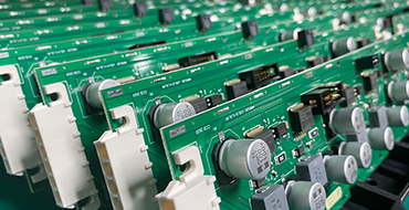
1. Line Width (Trace Width) Rules
Line width is the physical width of copper traces on your PCB. It directly affects current-carrying capacity, impedance control, and manufacturability.
1.1 Standard Minimum Trace Width
- Industry Standard: The most common minimum trace width for standard PCBs is 0.006 inch (6 mil / 0.152 mm). This is widely supported by low-cost prototyping and volume manufacturers.
- Advanced Capabilities: For high-density designs (HDI), advanced fabs can achieve 3 mil (0.076 mm) or even 2 mil (0.050 mm) lines, but expect higher costs and longer lead times.
- Extreme Precision: Some specialized manufacturers offer 1 mil (0.025 mm) trace/space for ultra-fine pitch BGA breakout, but this requires advanced laser direct imaging (LDI) and is not recommended for general use.
1.2 Current Carrying Capacity (IPC-2152)
- Copper Weight Matters: For standard 1 oz/ft² copper, a 10 mil trace can safely carry about 1.0 A (with 10°C temperature rise). For 2 oz copper, the same trace can carry ~1.5 A.
- Derating for High Temperatures: In environments above 85°C, reduce current ratings by 20-30%.
- Power Traces: For high-current paths (e.g., power supplies), use a trace width calculator or the IPC-2152 nomograph. A general rule: 1 oz copper, 20°C rise: 1A per 10 mil width is a conservative starting point.
1.3 Impedance-Controlled Traces
- Microstrip (Outer Layer): For 50Ω impedance on standard FR4 (εr ~4.5, 1 oz copper), typical trace width is 10-12 mil with a dielectric thickness of ~5 mil.
- Stripline (Inner Layer): For 50Ω stripline, trace width is typically 6-8 mil with equal prepreg/core thickness on both sides.
- Tolerance: Impedance tolerance should be ±10% for most digital signals, ±5% for RF. Inform your manufacturer if impedance control is required.
1.4 Differential Pair Trace Width
- USB 2.0: 90Ω differential impedance; typical width 8-10 mil with 8-10 mil spacing.
- HDMI/DVI: 100Ω differential; width ~6 mil with 6 mil spacing.
- Ethernet (100BASE-TX): 100Ω differential; width ~8 mil with 8 mil spacing.
- Important: Differential pair width and spacing must be calculated based on your stackup. Never guess—use a field solver.
1.5 Trace Width for High-Voltage
- Clearance vs. Width: For voltages >30V, trace width is less critical than spacing. However, ensure trace width can handle the current without excessive IR drop.
- Creepage: For mains voltage (110-240V AC), maintain at least 8 mm creepage distance between primary and secondary sides.
2. Spacing (Clearance) Rules
Spacing refers to the distance between copper features (traces, pads, planes, vias). Insufficient spacing can cause shorts, leakage, or breakdown.
2.1 Minimum Spacing (Standard)
- General Rule: 6 mil (0.152 mm) is the industry-standard minimum spacing for low-voltage digital/analog designs. This is safe for most manufacturers.
- High-Density: For BGA breakout or dense routing, 4 mil (0.102 mm) or 3 mil (0.076 mm) spacing is possible with advanced fabs, but expect a 10-20% cost premium.
- Ultra-Fine: 2 mil (0.050 mm) spacing is available for HDI but requires strict process control.
2.2 Voltage-Based Spacing (IPC-2221)
- Up to 15V: 0.1 mm (4 mil) minimum.
- 15V to 30V: 0.2 mm (8 mil) minimum.
- 30V to 50V: 0.4 mm (16 mil) minimum.
- 50V to 100V: 0.6 mm (24 mil) minimum.
- 100V to 250V: 1.5 mm (60 mil) minimum.
- 250V to 500V: 3.0 mm (120 mil) minimum.
- Important: These are bare-board clearances. For coated boards (conformal coating), distances can be reduced by 30-50%.
2.3 Creepage and Clearance for Safety (IEC/UL)
- Functional Insulation: For 250V AC, minimum 1.5 mm clearance, 2.5 mm creepage.
- Basic Insulation: 2.5 mm clearance, 4.0 mm creepage.
- Reinforced Insulation: 5.0 mm clearance, 8.0 mm creepage.
- Slots/Slits: If creepage distance is insufficient, add a slot in the PCB to increase the surface path.
2.4 Spacing for Different Net Classes
- Analog vs. Digital: Keep analog traces at least 10 mil away from high-speed digital traces to avoid noise coupling.
- Power vs. Signal: Maintain at least 10 mil spacing between power and low-level signal traces (e.g., sensor inputs).
- High-Impedance Nodes: For high-impedance analog inputs (e.g., op-amp inputs), use 20 mil minimum spacing to reduce leakage.
2.5 Pad-to-Pad and Pad-to-Trace Spacing
- SMD Pads: Minimum 6 mil between adjacent SMD pads (e.g., 0.5 mm pitch QFP). For 0.4 mm pitch, use 4 mil spacing.
- Through-Hole Pads: Keep at least 10 mil between the annular ring of one through-hole pad and the pad of another.
- Pad to Trace: Maintain at least 6 mil from the edge of a pad to an adjacent trace. For high-voltage, increase to 20 mil.
2.6 Copper-to-Board Edge Spacing
- Inner Layers: Keep copper at least 10 mil from the board edge.
- Outer Layers: Keep copper at least 12 mil from the board edge. For high-voltage, use 20 mil.
- Plated Edge: If you need copper near the edge (e.g., edge connectors), specify a plated edge (castellation) which adds 0.5 mm to the board outline.
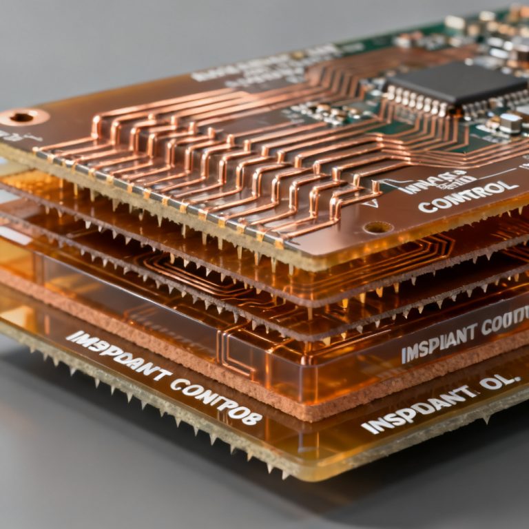
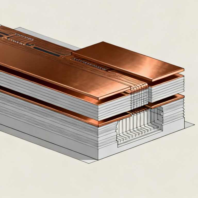
3. Via Sizes Rules
Vias are critical for connecting layers. Incorrect via sizing can cause manufacturing defects, signal integrity issues, or mechanical failure.
3.1 Standard Via Sizes
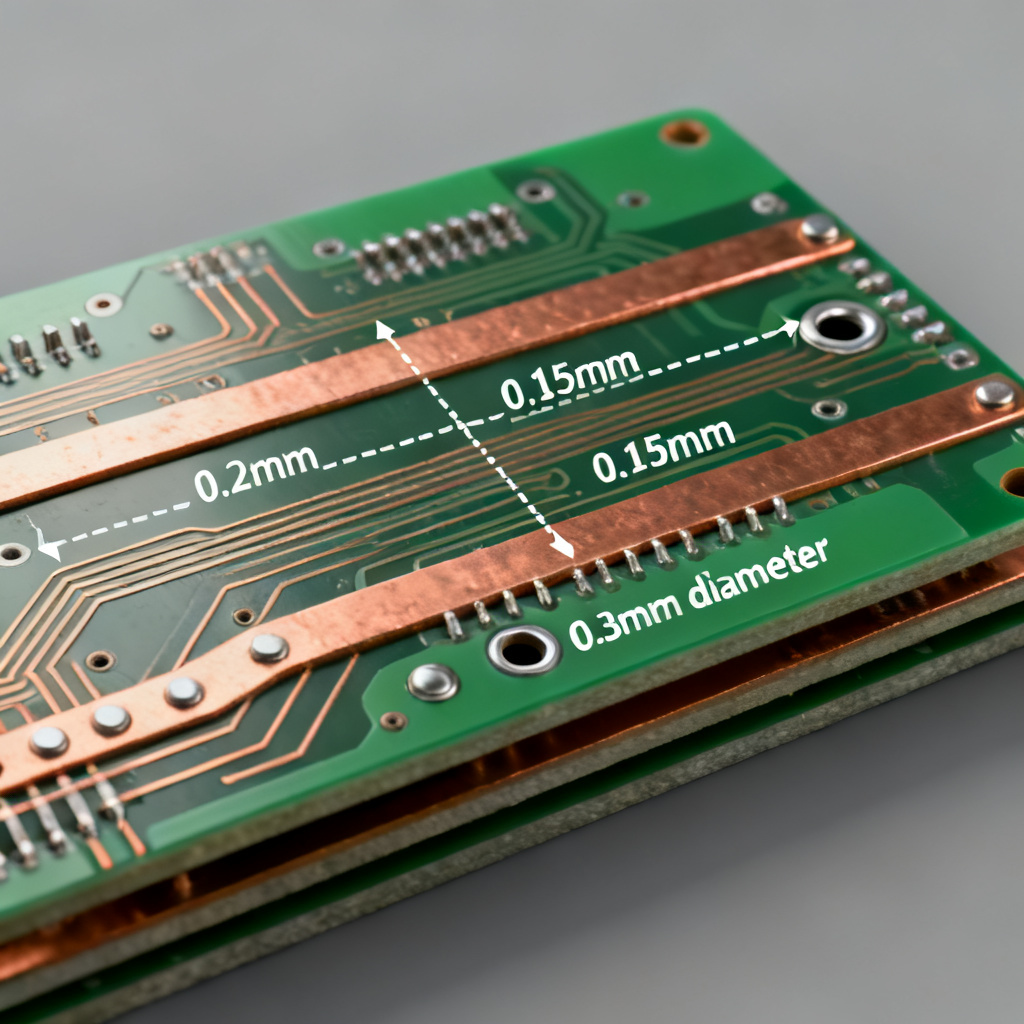
- Drill Size (Finished Hole): The most common standard via drill size is 0.3 mm (12 mil) . This is widely supported and cost-effective.
- Pad Diameter (Annular Ring): For a 0.3 mm drill, the pad diameter should be at least 0.6 mm (24 mil) , giving a 0.15 mm (6 mil) annular ring.
- Minimum Annular Ring: 4 mil (0.102 mm) is the absolute minimum for reliable manufacturing. 5-6 mil is recommended for high yield.
- Maximum Drill Size: For standard vias, 0.8 mm (32 mil) is typical. Larger than 1.0 mm (40 mil) may require special tooling.
3.2 Microvias (HDI)
- Laser Drilled: Microvias are typically 0.1 mm (4 mil) to 0.15 mm (6 mil) in drill diameter.
- Pad Diameter: For a 0.1 mm microvia, the pad should be at least 0.25 mm (10 mil).
- Aspect Ratio: For microvias, the aspect ratio (depth/diameter) should be ≤ 1:1. For example, a 0.1 mm drill can only go through a 0.1 mm dielectric layer.
- Stacked vs. Staggered: Stacked microvias (directly on top of each other) require filled and plated vias. Staggered microvias are easier to manufacture.
3.3 Via Aspect Ratio
- Standard Vias: The maximum aspect ratio for through-hole vias is 10:1 (e.g., 0.3 mm drill through a 3.0 mm board). For high reliability, keep it ≤ 8:1.
- HDI: For microvias, aspect ratio should be ≤ 1:1.
- Buried/Blind Vias: Aspect ratio should be ≤ 1:1 for blind vias, ≤ 2:1 for buried vias.
3.4 Via Current Capacity
- Rule of Thumb: A 0.3 mm (12 mil) via with 1 oz copper plating can carry approximately 1.0 A with a 20°C temperature rise.
- Plating Thickness: Standard via plating is 20-25 µm (0.8-1.0 mil) . For higher current, specify 35 µm (1.4 mil) plating.
- Multiple Vias: For high-current paths, use multiple vias in parallel (e.g., 3-4 vias for a 3A trace). Place them close to the power pin.
3.5 Via-in-Pad (VIP) Rules
- Filled Vias: If you place a via directly in an SMD pad (e.g., for thermal management), it must be filled with non-conductive epoxy and plated over (capped). Unfilled vias will cause solder wicking and tombstoning.
- Pad Size: For a via-in-pad, the pad diameter must be at least 0.1 mm larger than the via’s finished hole size.
- Thermal Relief: For vias connected to large copper planes (e.g., ground), use a thermal relief pattern (4 spokes, 8-10 mil wide) to avoid soldering issues.
3.6 Via Clearance (Antipad)
- Antipad Size: For a via passing through a copper plane (e.g., ground plane), the antipad (clearance hole) should be at least 10 mil larger in diameter than the via pad. For high-voltage, increase to 20 mil.
- Impedance Control: For controlled impedance, the antipad size must be calculated to maintain the correct impedance (e.g., for a 50Ω stripline via, the antipad may need to be 30 mil larger).
3.7 Via Tenting
- Tenting (Covering): Vias can be tented with solder mask to prevent oxidation and shorting. Ensure the via’s annular ring is small enough (≤ 0.5 mm pad) to allow full tenting.
- Uncovered Vias: For test points or high-current vias, leave them uncovered. Specify “via not tented” in your fabrication notes.
4. General DFM Checklist (Combined from Top Sources)
To ensure your design is manufacturable, review this final checklist before sending Gerbers:
4.1 Minimum Requirements (All Manufacturers)
- Minimum trace width: 6 mil (0.152 mm)
- Minimum spacing: 6 mil (0.152 mm)
- Minimum drill size: 0.3 mm (12 mil)
- Minimum annular ring: 4 mil (0.102 mm)
- Copper-to-edge spacing: 10 mil (0.254 mm) inner, 12 mil (0.305 mm) outer
- Board thickness: 1.6 mm (standard), 0.8-2.4 mm typical
- Copper weight: 1 oz (35 µm) standard, 2 oz (70 µm) for power
4.2 Advanced Capabilities (Check with Manufacturer)
- Trace/space: 3/3 mil (0.076/0.076 mm) for HDI
- Microvia drill: 0.1 mm (4 mil)
- Blind/buried vias: Confirm stackup and aspect ratio
- Via-in-pad: Specify filled and capped
- Impedance control: ±10% tolerance, provide stackup
- Gold plating (ENIG): 0.05-0.1 µm gold over 3-5 µm nickel
4.3 Signal Integrity Checklist
- Differential pairs: Width and spacing calculated for target impedance
- Critical nets: Keep away from noisy traces (clocks, switching regulators)
- Return path: Ensure continuous ground plane under high-speed traces
- Via stitching: Add ground vias adjacent to signal vias at layer transitions
- Length matching: For high-speed buses (e.g., DDR), match trace lengths within 50 mil
4.4 Mechanical & Assembly Checklist
- Solder mask clearance: 2-3 mil smaller than pad (to avoid slivers)
- Silkscreen: Keep off pads and vias (at least 5 mil clearance)
- Mounting holes: Use non-plated holes for mechanical mounting, plated for grounding
- Panelization: Add mouse bites or V-score lines for depanelization
- Fiducials: Add three global fiducials (1 mm diameter, uncoated copper) for pick-and-place
5. Final Expert Tips from the Industry Leaders
- From Altium: “Always run a design rule check (DRC) with your manufacturer’s capabilities loaded. Do not assume your default rules are correct. Use the IPC-2221 and IPC-2152 standards as a baseline, then adjust for your specific manufacturer.”
- From Sierra Circuits: “The most common DFM issues are annular ring violations and trace-to-edge spacing. Always add a 0.5 mm keepout zone around the board outline. For high-voltage designs, use a slot or a routed groove to increase creepage distance.”
- From PCBWay: “If you are unsure about a rule, ask your manufacturer before ordering. We can often relax or tighten rules based on your specific needs. For example, we can do 4/4 mil trace/space for a small cost increase, but 3/3 mil requires a different process. Communication saves time and money.”
6. How to Use This Checklist for Your Next Project
- Download the checklist (or copy it into your design notes).
- Set your CAD rules (e.g., Altium, KiCad, Eagle) to match the standard values first.
- Run a DRC after routing to catch violations.
- Send your Gerbers to your manufacturer (like us) with a note specifying any critical requirements (e.g., impedance, via-in-pad, high-voltage).
- Review the manufacturer’s DFM report and adjust if needed.

Need a Reliable Partner for Your PCB Fabrication?
We are a professional B2B PCB manufacturer specializing in low-cost prototyping to high-volume production. Our capabilities include:

- Standard 6/6 mil trace/space (4/4 mil for HDI)
- 0.3 mm minimum drill (0.15 mm microvias available)
- 1-32 layer boards, FR4, high-Tg, and flex
- ENIG, HASL, OSP, and immersion silver finishes
- Full DFM review with free feedback
Request a quote today and let us help you turn your design into a reliable, high-yield product. Email us at [sales@yourdomain.com] or use our online quote tool.
Design Rules Checklist: Line Width, Spacing & Via Sizes
A practical PCB reference for manufacturability, signal integrity, current capacity, and via reliability—consolidating standard DFM values and advanced fabrication considerations into one engineering-ready guide.
PCB Design Rules That Protect Yield, Cost, and Performance
When designing a printed circuit board, line width, spacing, and via dimensions are not just CAD settings—they define whether your board can be fabricated reliably, assembled cleanly, and perform as intended in the field. This guide consolidates practical baseline values and advanced considerations into one readable engineering reference.
1. Line Width Rules
Trace width affects current capacity, impedance, copper loss, and manufacturability. Your final width should reflect both electrical and fabrication constraints.
1.1 Standard Minimum Trace Width
- 6 mil (0.152 mm) is the most common standard minimum for general-purpose boards.
- 3 mil to 4 mil routing is often available for dense layouts with cost premium.
- 2 mil and below typically require advanced HDI capability and strict process control.
1.2 Current Carrying Capacity
- For 1 oz copper, a 10 mil trace is often used as a conservative starting point for around 1 A depending on temperature rise and layer location.
- Higher ambient temperatures and enclosed products require derating.
- Use IPC-2152-based calculators for power traces instead of relying on guesswork.
1.3 Controlled Impedance and Differential Pairs
Controlled impedance traces depend on stackup, dielectric thickness, copper weight, and reference plane geometry. For differential pairs such as USB, HDMI, or Ethernet, both width and spacing must be calculated from the actual stackup.
2. Spacing Rules
Spacing or clearance governs short-circuit risk, dielectric breakdown, leakage, and noise coupling between nets.
2.1 Standard Minimum Spacing
- 6 mil is the standard baseline for low-voltage digital and analog layouts.
- 4 mil to 3 mil is possible in dense routing with advanced fabrication.
- 2 mil spacing should be treated as a specialized HDI capability, not a default rule.
2.2 Voltage-Based Clearance
Higher voltage requires larger air clearance and surface creepage distances. IPC-2221 provides a baseline, but safety-critical applications may need IEC or UL-driven rules beyond general PCB fabrication standards.
2.3 Practical Layout Separation
- Keep analog traces away from noisy digital or switching nodes.
- Maintain extra spacing for high-impedance analog inputs to reduce leakage.
- Increase copper-to-edge spacing beyond standard values when handling higher voltage or panel stress.
3. Via Sizes Rules
Vias connect layers electrically, but poor via choices can create plating, reliability, or assembly problems.
3.1 Standard Via Sizes
- 0.3 mm finished drill is a common, economical standard.
- 0.6 mm pad diameter is a practical match for a 0.3 mm drill.
- 4 mil annular ring is often treated as an absolute lower limit; 5–6 mil is safer for yield.
3.2 Microvias and HDI
- Microvias are typically laser-drilled at 0.1 mm to 0.15 mm.
- Aspect ratio should generally remain at or below 1:1.
- Stacked microvias are more complex and often require filled and plated structures.
3.3 Via Current and Antipad
Current capacity depends on drill size, plating thickness, and temperature rise. For vias passing through planes, the antipad must be large enough for manufacturability and may need tuning for impedance-controlled structures.
4. General DFM Checklist
- Minimum trace width: 6 mil
- Minimum spacing: 6 mil
- Minimum drill size: 0.3 mm
- Minimum annular ring: 4 mil
- Inner copper to edge: 10 mil minimum
- Outer copper to edge: 12 mil minimum
- Standard board thickness: 1.6 mm
- Typical copper weight: 1 oz, with 2 oz used for power where needed
5. Final Expert Tips
Always run DRC using your manufacturer’s actual capabilities, not only default CAD settings. For controlled impedance, blind/buried vias, via-in-pad, high voltage, or HDI routing, confirm stackup and rule limits before release. Early fab communication prevents costly redesign cycles.
6. How to Use This Checklist
- Start with standard manufacturable rules in your CAD tool.
- Adjust nets by class for impedance, voltage, and current needs.
- Run DRC after placement and again after routing.
- Submit Gerbers with fabrication notes for critical constraints.
- Review the DFM report and revise before production release.
We support standard and advanced fabrication workflows, including DFM review, HDI capabilities, controlled impedance, and production-ready engineering feedback.
Request a Quote