PCB Parameters Specifications A Complete Engineering Reference
This complete engineering reference consolidates all critical PCB Parameters Specifications A Complete Engineering Reference from IPC standards, leading manufacturers, and design authorities. Whether you are a design engineer or procurement specialist, this guide provides the definitive technical details for specifying and ordering PCBs with confidence.
1. Core PCB Parameters & Specifications: The Foundation of Design
Layer Count & Stackup Configuration
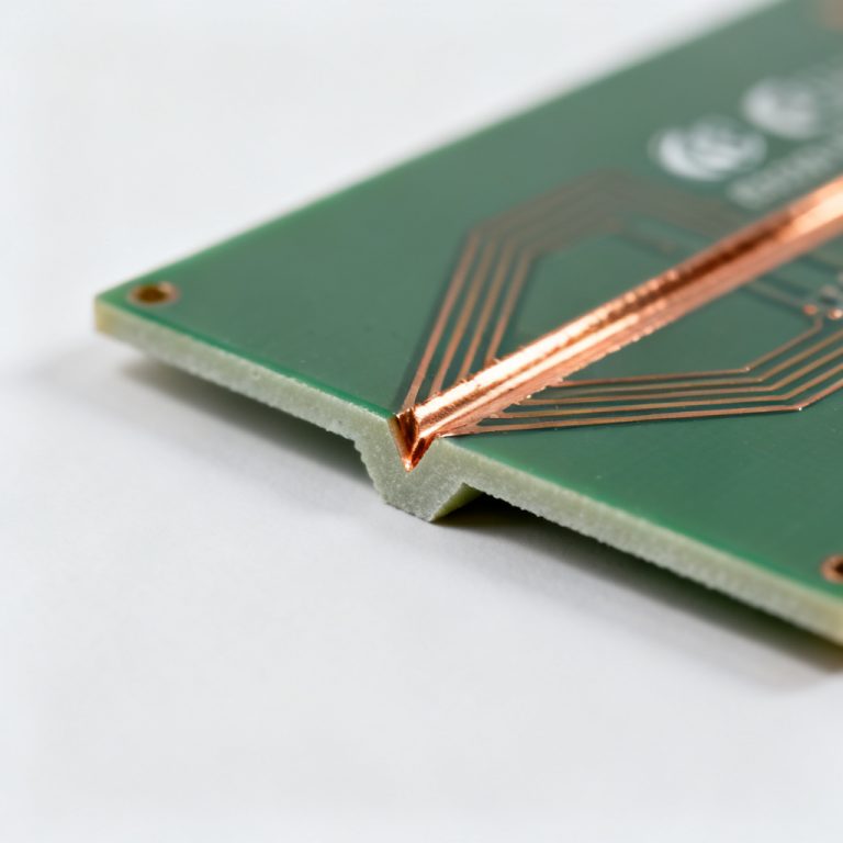
PCB parameters and specifications begin with layer count: the number of conductive copper layers including signal, ground, and power planes. Standard range is 1-layer to 64+ layers. Common stackups include 2-layer FR-4, 4-layer for most digital designs, and 6-8 layer for complex mixed-signal or high-speed boards. Per IPC-6012, a 4-layer board typically uses a 0.031” core with prepreg layers. Always specify target impedance (e.g., 50Ω single-ended, 100Ω differential) and dielectric constant (Dk) for controlled impedance stackups.
Board Thickness & Tolerance
Standard PCB thickness is 1.6mm (0.062”) for FR-4, ranging from 0.2mm to 6.0mm. IPC-6012 Class 2 tolerance: ±10% for thickness ≤1.0mm; ±0.1mm for 1.0-2.5mm; ±0.15mm for >2.5mm. Thin boards (<0.8mm) require stiffeners for component mounting.
Copper Weight (Thickness)
Copper weight is measured in oz/ft²: 0.5 oz (18 µm) for fine-pitch SMT, 1 oz (35 µm) most common, 2 oz (70 µm) for power traces, 3-4 oz for heavy copper. Tolerance: ±0.5 oz for 1 oz base copper; ±1 oz for 2 oz+. Inner layer copper is typically lighter (0.5 or 1 oz) due to etching limitations.
2. Material Specifications: Choosing the Right Substrate
Material Types & Their Properties
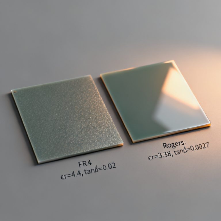
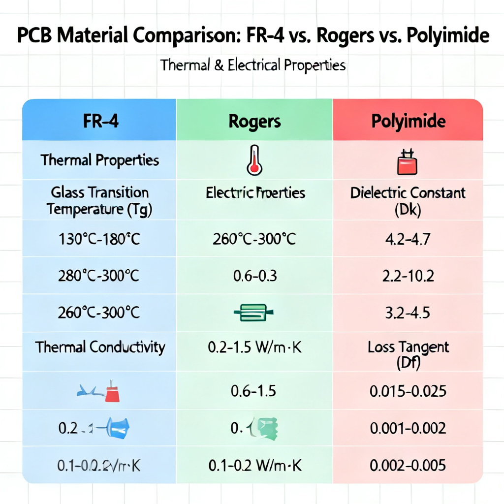
PCB parameters and specifications for materials include FR-4 (standard, Tg 130-140°C), High-Tg FR-4 (>170°C, e.g., Isola 370HR), Polyimide (Tg >250°C, flexible), Rogers high-frequency laminates (low Df, stable Dk), Aluminum MCPCB for thermal management, and Flex/Rigid-Flex polyimide films.
Key Material Parameters (From IPC-4101)
Glass Transition Temperature (Tg): >140°C standard, >170°C high-reliability. Decomposition Temperature (Td): >300°C for high-performance. Dielectric Constant (Dk): FR-4 4.2-4.8 at 1 MHz; specify tolerance ±0.2 for impedance control. Dissipation Factor (Df): <0.02 for high frequencies. Moisture Absorption: <0.5% for FR-4. CTE: Z-axis <70 ppm/°C standard, <50 ppm/°C for high-Tg.
3. Dimensional & Mechanical Specifications
Board Outline & Dimensions
Maximum size typically 20” x 24”; minimum no absolute but <10mm requires panelization. Tolerance: ±0.1mm standard routing; ±0.05mm laser/precision. Shape: rectangular, circular, or irregular.
Hole Specifications
Plated Through-Holes (PTH): minimum 0.2mm standard, 0.1mm microvia; tolerance ±0.05mm PTH, ±0.025mm microvia; aspect ratio max 10:1 standard, 20:1 specialized. Non-Plated Through-Holes (NPTH): minimum 0.3mm; tolerance ±0.05mm. Slot holes: minimum width 0.4mm.
Panelization & Breakaway Tabs
Tab routing: V-groove for straight edges, mouse bites for irregular shapes. Rail width 5-10mm. Tooling holes: at least 2 NPTH 3mm diameter on panel edge.
4. Electrical Specifications & Tolerance
Controlled Impedance
PCB parameters and specifications for controlled impedance ensure consistent characteristic impedance (e.g., 50Ω, 100Ω). Methods: microstrip (outer) and stripline (inner). Tolerance: ±10% standard; ±5% high-speed per IPC-2141. Key factors: trace width, copper thickness, dielectric height, Dk.
Current Carrying Capacity
Per IPC-2221/2222, formula I = k * (T^0.44) * (A^0.725). Typical values (1 oz copper, 10°C rise): 10 mil trace ~1.0A outer, ~0.5A inner; 50 mil ~2.5A outer, ~1.2A inner; 100 mil ~4.0A outer, ~2.0A inner. Use wider traces or heavier copper for high-current.
Voltage & Clearance (Creepage & Clearance)
Minimum clearance per IPC-2221: <50V 0.1mm external, 0.05mm internal; 50-150V 0.2mm external, 0.1mm internal; 150-300V 0.3mm external, 0.2mm internal; >300V use Table 6-1. Creepage typically 1.5x clearance. Dielectric withstanding voltage >40 kV/mm for FR-4.
5. Manufacturing Tolerances & Quality Classes
IPC-6012 Class Definitions
Class 1 (General): ±20% tolerances. Class 2 (Dedicated Service): ±10%, standard for industrial/automotive. Class 3 (High Reliability): ±5% or tighter, for aerospace/medical. Class 3/A (Space/Avionics): most stringent, 100% electrical test and X-ray.
| Parameter | Class 1 | Class 2 | Class 3 |
|---|---|---|---|
| Hole Diameter (PTH) | ±0.1mm | ±0.08mm | ±0.05mm |
| Trace Width (outer) | ±20% | ±15% | ±10% |
| Spacing (outer) | ±20% | ±15% | ±10% |
| Annular Ring (outer) | 0.1mm min | 0.15mm min | 0.2mm min |
| Bow & Twist | 1.5% | 1.0% | 0.75% |
Registration & Alignment
Layer-to-layer: ±0.1mm Class 2; ±0.075mm Class 3. Solder mask registration: ±0.1mm standard; ±0.05mm fine-pitch. Silkscreen: ±0.2mm.
6. Surface Finish Options & Specifications
Common Finishes (From IPC-4552, 4553, 4554)
HASL (leaded or lead-free): thickness 1-40 µm, good shelf life 12 months, not for fine-pitch <0.5mm. ENIG: nickel 3-6 µm, gold 0.05-0.15 µm immersion, 0.5-1.0 µm electrolytic for edge connectors. OSP: 0.2-0.5 µm, low cost, short shelf life 6 months. Immersion Silver: 0.15-0.5 µm, good for high-frequency. Immersion Tin: 0.8-1.2 µm, for press-fit. Hard Gold: 0.5-2.0 µm over nickel for edge connectors.
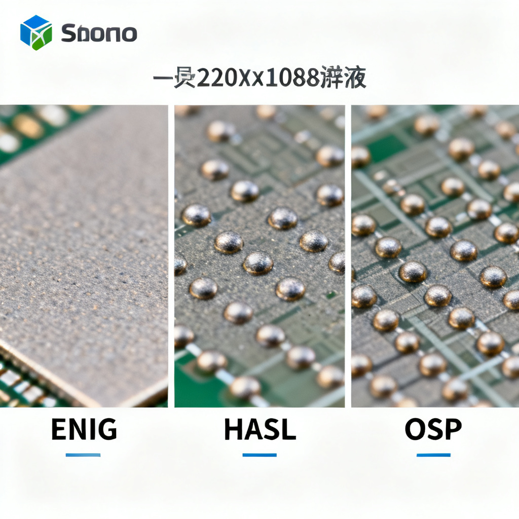
Finish Selection Guide
Fine-pitch (BGA, QFN): ENIG or Immersion Silver. High-temperature: ENIG or HASL lead-free. Cost-sensitive: HASL or OSP. Wire bonding: ENIG or Hard Gold. Edge connectors: Hard Gold.
7. Solder Mask & Silkscreen Specifications
Solder Mask (IPC-SM-840)
Types: LPI most common, dry film for fine-pitch, flexible for flex PCBs. Colors: green, blue, red, black, white, yellow. Thickness: 0.3-0.5 mm over copper, 0.1-0.2 mm on bare laminate. Clearance (dam): minimum 0.05mm fine-pitch, 0.1mm standard. Registration: ±0.1mm Class 2; ±0.05mm Class 3.
Silkscreen (Legend)
Color: white most common. Line width: minimum 0.15mm standard, 0.1mm fine. Text height: minimum 0.8mm standard, 0.6mm fine. Registration: ±0.2mm. Avoid silkscreen over pads or vias.
8. Testing & Quality Assurance Specifications
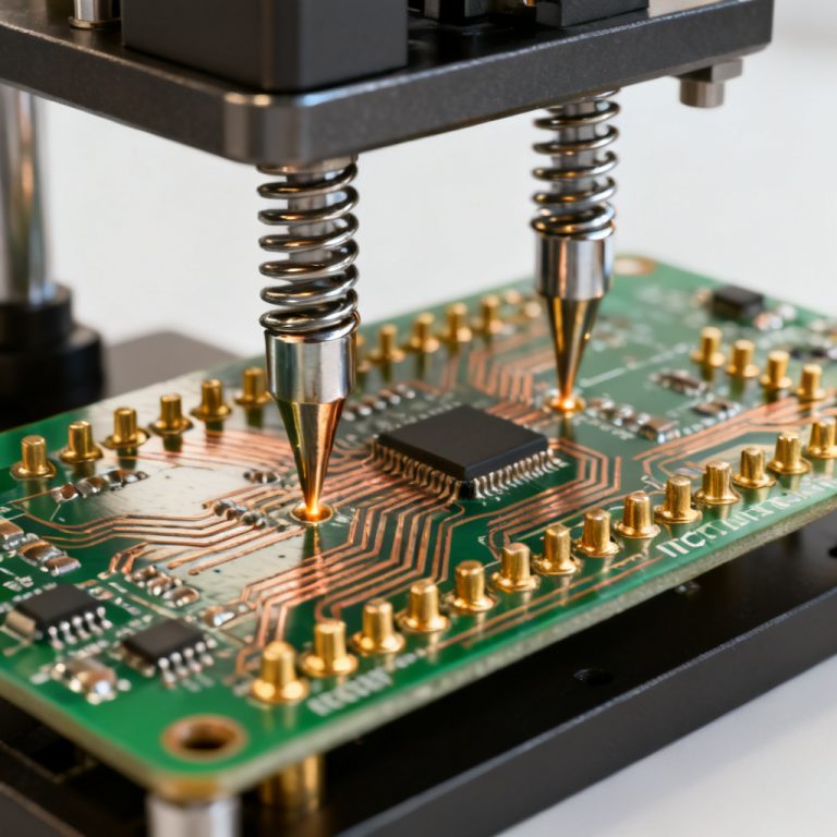
Electrical Testing
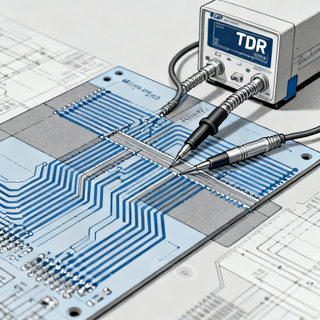
Types: flying probe (prototypes), fixture-based (high volume). Parameters: continuity, resistance, capacitance, impedance (TDR). Test voltage: 250VAC/500VDC Class 2; 500VAC/1000VDC Class 3. Coverage: 100% for Class 2/3.
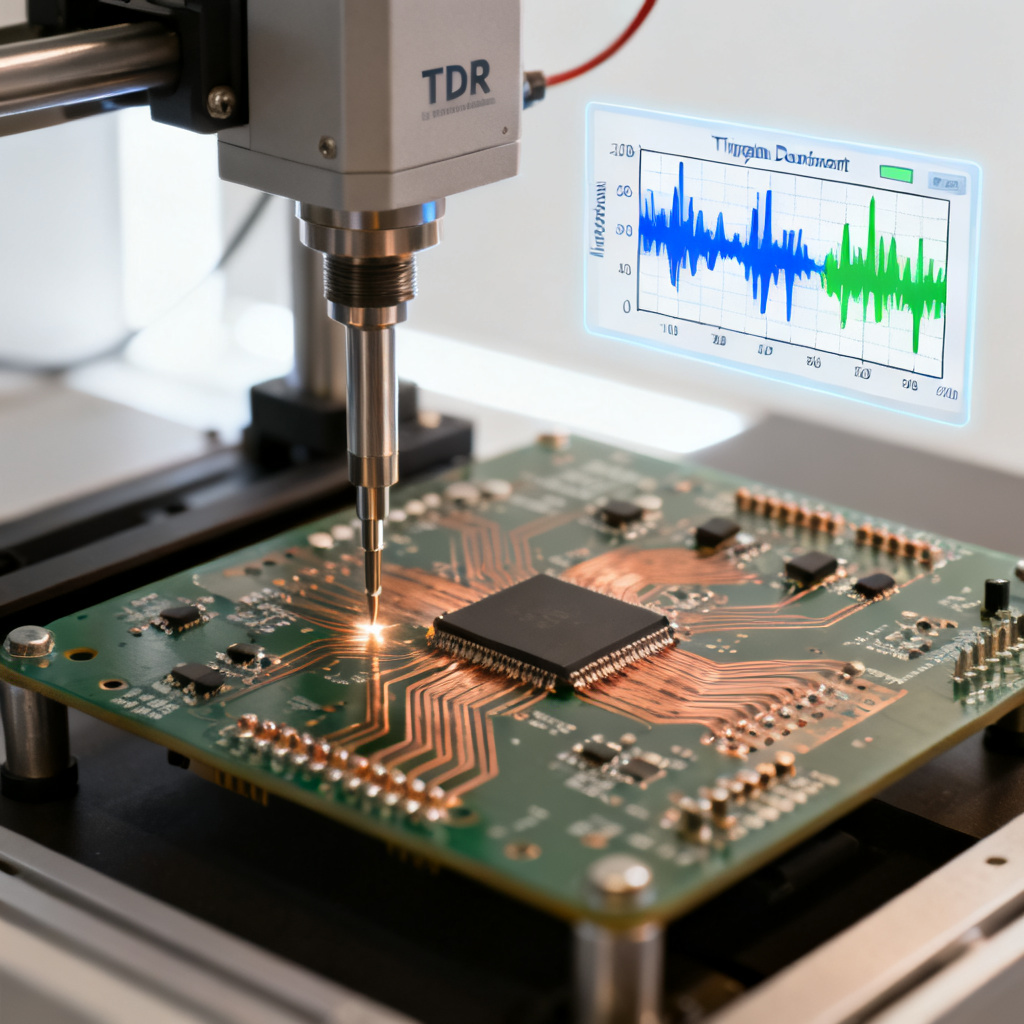
Impedance Coupon Testing
Per IPC-2141, coupon must replicate stackup and trace geometry. Tolerance: ±10% standard; ±5% high-speed.
Thermal Stress Testing
Solder float: 260°C/10s Class 2; 288°C/10s Class 3. No delamination or blistering. Thermal cycling: -40°C to +125°C, 100 cycles for Class 3.
Visual & Dimensional Inspection
Per IPC-A-600: no solder mask voids >0.5mm, no copper scratches >10% trace width, no silkscreen smearing. Dimensional check per IPC-2615.
9. Advanced Specifications for High-Performance PCBs
Microvias & HDI
Microvia size: 0.1mm minimum; 0.075mm advanced. Aspect ratio ≤1:1 standard; ≤2:1 laser. Stacked microvias for via-in-pad BGA. Blind/buried vias connect outer/inner layers.
Via-in-Pad (VIP) & Plugging
Filling: non-conductive epoxy (soldering) or conductive (thermal/electrical). VIP must be filled and copper-capped. Via diameter ≤0.3mm; fill depth >50% board thickness.
Thermal Management
Thermal vias: arrays under heat-generating components. Copper coin: embedded thick copper. Metal Core (MCPCB): aluminum/copper base, thin dielectric 0.1-0.2mm, thermal conductivity 1-3 W/mK. TIM for heat sinks.
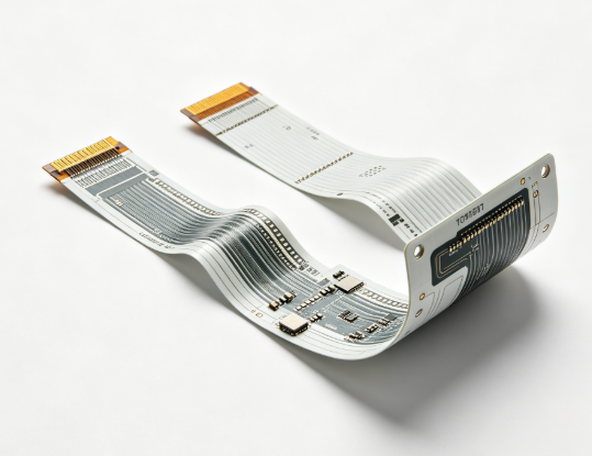
Flex & Rigid-Flex Specifications
Flex material: polyimide (Kapton). Bend radius: 10x thickness dynamic, 5x static. Coverlay: 0.025-0.075mm polyimide. Stiffeners: FR-4, polyimide, or metal. Rigid-flex transition zone gradual.
10. Documentation & File Format Specifications
Required Files for PCB Manufacturing
Gerber RS-274X: each layer as .gbr. Drill Excellon: .drl. Netlist IPC-356: for electrical test. Readme: stackup, impedance, special instructions.
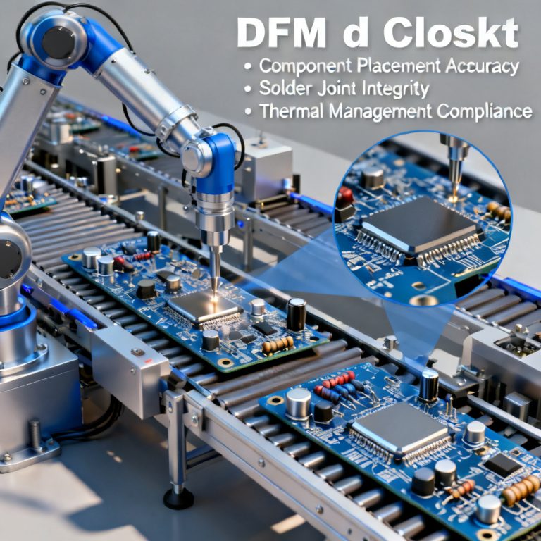
Design for Manufacturing (DFM) Checklist
Minimum trace/spacing: 6/6 mil standard, 4/4 mil advanced. Annular ring: 0.15mm minimum Class 2. Copper to edge: 0.3mm. Solder mask to pad: 0.05mm. Silkscreen to pad: 0.2mm. Vias under BGA: via-in-pad or tenting.
FAQ: PCB Parameters & Specifications
What are the most critical PCB parameters and specifications for a standard design?
The most critical PCB parameters and specifications include layer count, board thickness, copper weight, material type (FR-4 with Tg >140°C), trace/space minimums, hole sizes, and surface finish (ENIG or HASL).
How do I specify controlled impedance in my PCB parameters and specifications?
To specify controlled impedance, include target impedance (e.g., 50Ω), stackup details, dielectric constant (Dk), trace width, and copper thickness in your PCB parameters and specifications. Use IPC-2141 coupon testing for verification.
What is the difference between IPC Class 2 and Class 3 in PCB parameters and specifications?
IPC Class 2 allows ±10% tolerances for most PCB parameters and specifications, suitable for industrial use. Class 3 requires ±5% or tighter, with 100% electrical test and stricter criteria for aerospace/medical.
Which surface finish is best for fine-pitch components per PCB parameters and specifications?
For fine-pitch components like BGA or QFN, ENIG (Electroless Nickel Immersion Gold) is recommended in PCB parameters and specifications due to its flat surface and excellent solderability.
How do I choose the right material for high-frequency PCB parameters and specifications?
For high-frequency designs, select materials with low Df and stable Dk, such as Rogers laminates. Include these in your PCB parameters and specifications to ensure signal integrity.
Why Our PCB Parameters & Specifications Service Stands Out
We provide comprehensive PCB parameters and specifications support from prototype to production, with free DFM review, Class 2/3 quality, and fast turnaround for export orders. Unlike generic manufacturers, we offer detailed engineering guidance on material selection, impedance control, and advanced HDI technologies.