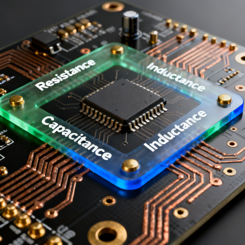
Electrical Parameters Resistance Capacitance Inductance
Master the critical Electrical Parameters Resistance Capacitance Inductance in PCB design. Understand their physical origins, impact on signal integrity, impedance control, parasitic effects, and practical mitigation strategies for high-speed, high-frequency, and power applications. This essential guide serves B2B PCB engineers and buyers seeking deep technical knowledge.
1. Resistance (R) – The Conductor’s Opposition to Current Flow
1.1 The Physics of Resistance
Electrical Parameters – Resistance, Capacitance, Inductance begin with resistance, the measure of a material’s opposition to electric current. In a PCB, this applies to copper traces, vias, and component leads. The fundamental relationship is Ohm’s Law: V = I × R. However, for PCB designers, the critical equation is the resistivity formula: R = ρ × (L / A).
Where ρ is the resistivity of the conductor (copper: ~1.68 × 10⁻⁸ Ω·m at 20°C), L is trace length, and A is cross-sectional area (trace width × copper thickness).
Key implications for PCBs:
- Copper Thickness: Standard PCB copper weights are 0.5 oz/ft², 1 oz/ft², and 2 oz/ft². Thicker copper (higher “oz” value) provides a larger cross-sectional area (A), reducing resistance. For high-current paths like power supplies and motor drives, 2 oz or heavier copper is essential.
- Trace Width: Wider traces have lower resistance. For a given current, calculate the minimum trace width to prevent excessive voltage drop and heat generation (I²R losses).
- Temperature Coefficient: Copper’s resistivity increases approximately 0.39% per °C. In high-power or high-temperature environments, resistance can increase significantly, leading to thermal runaway if not accounted for.
1.2 DC vs. AC Resistance (Skin Effect)
At low frequencies, current distributes uniformly across the entire conductor cross-section. However, at high frequencies (above ~1 MHz), the skin effect becomes dominant. Skin depth (δ) is defined as δ = √(2ρ / ωμ), where ω = 2πf and μ = permeability of the conductor.
At 1 GHz, skin depth in copper is approximately 2 μm, reducing the effective cross-sectional area to a thin outer “skin.” The AC resistance (R_AC) can be significantly higher than DC resistance (R_DC), especially for thick traces. Mitigation includes using wider traces to increase surface area or employing microstrip or stripline geometries. For very high frequencies, silver or gold plating (lower resistivity) reduces skin effect losses.
1.3 Resistance in PCB Design: Practical Considerations
- Voltage Drop (IR Drop): In power distribution networks (PDN), trace resistance causes voltage drops between the power supply and load. Use power integrity (PI) analysis tools to simulate IR drop and optimize trace widths, copper pours, and via stitching.
- Power Dissipation (I²R Loss): Heat generated by resistance can degrade component performance. For high-current paths, calculate required trace width using IPC-2221 standards or calculators like Saturn PCB Toolkit.
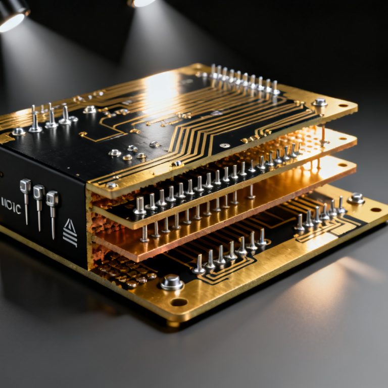
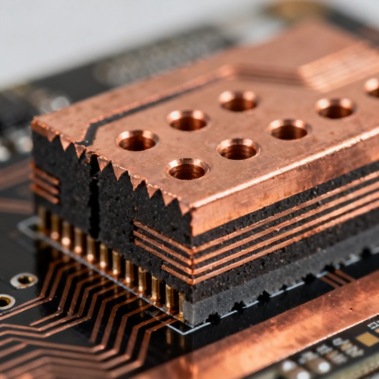
- Via Resistance: Vias are small plated holes connecting layers. Their resistance depends on plating thickness (typically 1 mil or 25 μm) and via diameter. Multiple vias in parallel (via stitching) reduce total resistance and improve current-carrying capacity.
- Contact Resistance: At connectors, test points, or solder joints, resistance can increase due to oxidation or contamination. Use gold-plated contacts for critical signals to maintain low and stable contact resistance.
1.4 Resistance in B2B PCB Manufacturing: What to Specify
When ordering PCBs, specify copper weight (e.g., 1 oz, 2 oz), trace width and spacing based on current and voltage requirements, via plating thickness (standard 20-25 μm, 35 μm or thicker for high-current), and surface finish (ENIG, HASL, OSP) which affects contact resistance and solderability.
2. Capacitance (C) – The Ability to Store Electrical Energy
2.1 The Physics of Capacitance
Electrical Parameters – Resistance, Capacitance, Inductance include capacitance, the ability of a system to store electric charge. In a PCB, capacitance exists between any two conductors separated by a dielectric. The fundamental equation for a parallel-plate capacitor is: C = ε₀ × εr × (A / d), where ε₀ is permittivity of free space, εr is relative permittivity (dielectric constant), A is overlapping conductor area, and d is distance between them.
Key implications for PCBs:
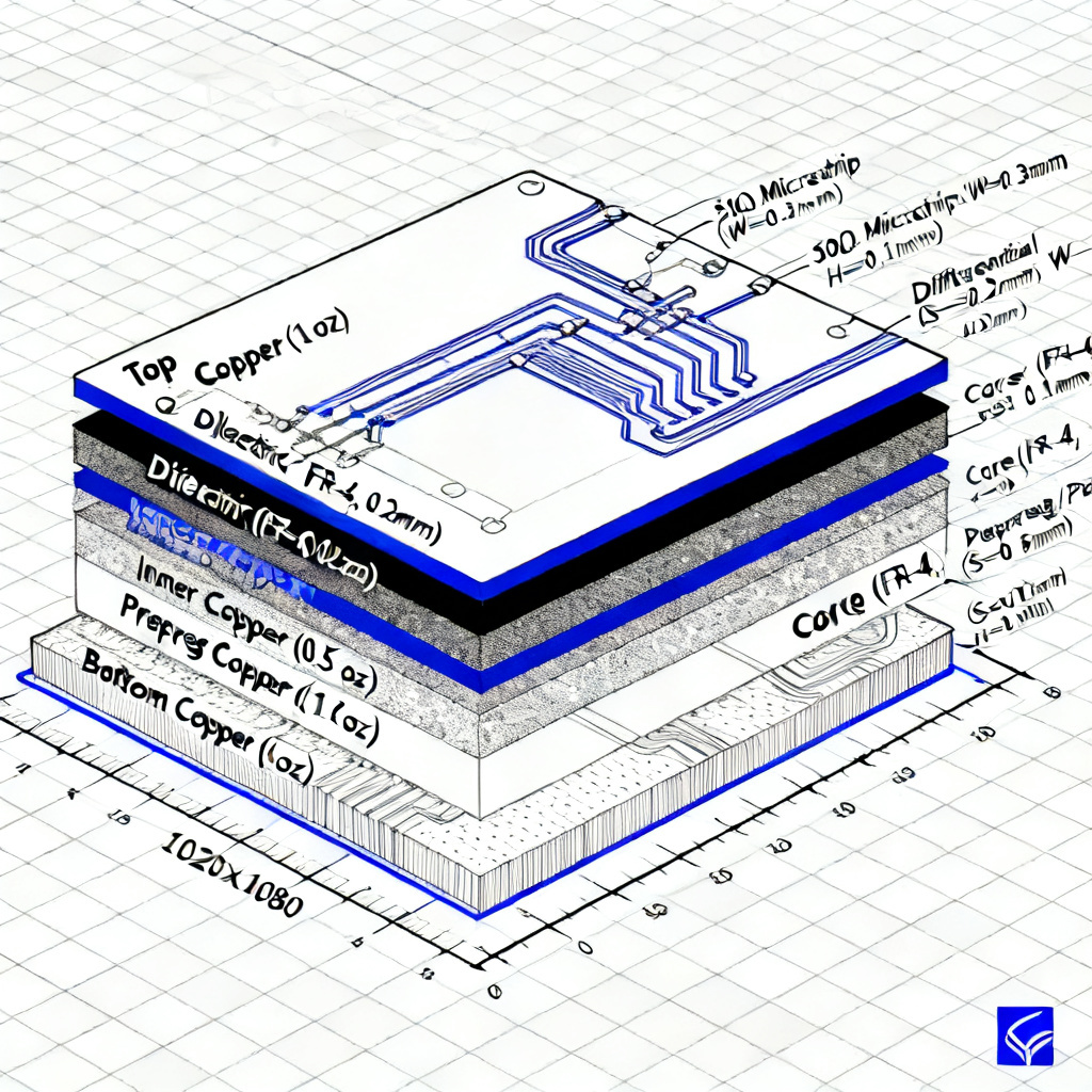
- Dielectric Material: Standard FR-4 has εr of approximately 4.2–4.8. High-frequency materials like Rogers or Isola have lower and more stable εr (e.g., 2.2–3.5).
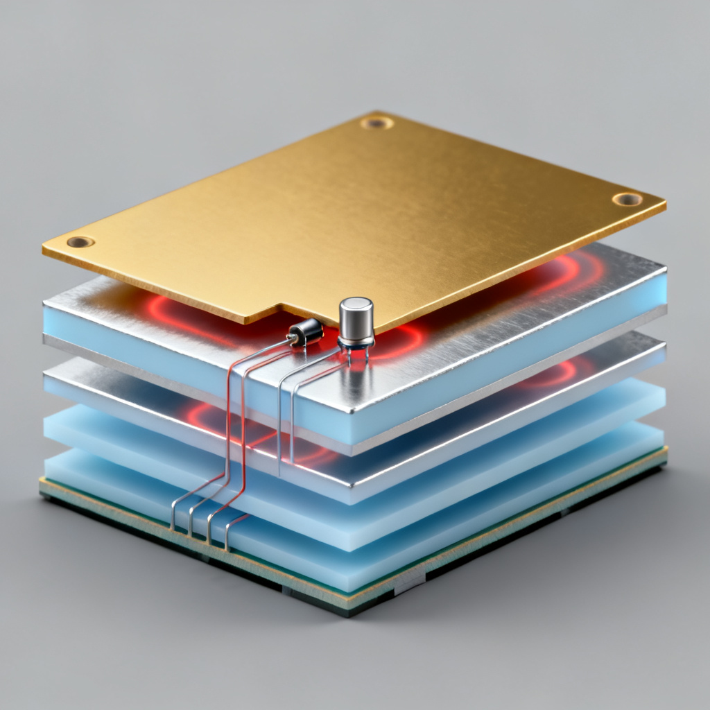
- Layer Stack-Up: Capacitance between power and ground planes is critical. A thinner dielectric (prepreg) increases distributed capacitance, helping decouple high-frequency noise and stabilize power supply.
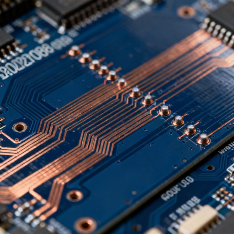
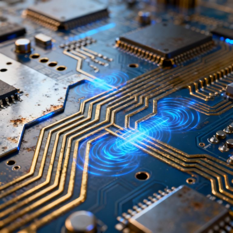
- Trace-to-Trace Capacitance: Adjacent traces form capacitors, causing parasitic crosstalk and signal degradation, especially in high-speed designs.
2.2 Parasitic Capacitance in PCB Design
Parasitic capacitance is unintended and often detrimental. Common sources include via-to-plane capacitance, pad-to-plane capacitance, and inter-trace capacitance. Mitigation strategies include increasing spacing between high-speed traces (3W rule: spacing = 3× trace width), using guard traces or ground planes between sensitive analog and digital signals, minimizing via length, and selecting low-Dk materials for high-frequency circuits.
2.3 Capacitance in Power Distribution Networks (PDN)
A well-designed PDN uses capacitance at multiple frequency ranges: bulk capacitors (10–100 μF) for low-frequency energy storage, ceramic capacitors (0.1 μF, 0.01 μF) for mid-frequency decoupling, and distributed capacitance from power/ground planes for high-frequency decoupling (>100 MHz). Every capacitor has a self-resonant frequency (SRF) where impedance is minimum; above SRF, it behaves inductively. A combination of capacitor values and types covers the entire frequency spectrum.
2.4 Capacitance in High-Speed and RF Design
For controlled impedance traces (e.g., 50 Ω microstrip), capacitance per unit length is key. Trace width, dielectric thickness, and εr determine characteristic impedance (Z₀ = √(L/C)). Capacitive discontinuities like via stubs and pads cause signal reflections; minimize stub lengths and use back-drilling for high-speed signals. In high-speed serial links (e.g., PCIe, USB 3.0), DC blocking capacitors (typically 0.1 μF) isolate DC bias levels; choose capacitors with low ESL and low ESR for minimal signal distortion.
2.5 B2B Specification Considerations for Capacitance
Specify dielectric material (FR-4 for general-purpose, high-frequency laminates like Rogers, Isola, Taconic for RF/microwave), prepreg thickness for controlled impedance with exact Dk tolerance, and stack-up design that optimizes distributed capacitance while minimizing parasitic effects.
3. Inductance (L) – The Tendency to Oppose Changes in Current
3.1 The Physics of Inductance
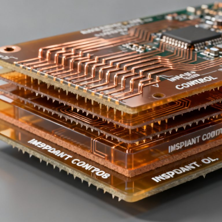
Electrical Parameters – Resistance, Capacitance, Inductance conclude with inductance, the property of a conductor to oppose change in current flow. Defined by Faraday’s Law, a changing current induces a back EMF opposing the change. The unit is Henry (H). In a PCB, inductance arises from the loop area formed by a current path and its return path. Loop inductance is key: L_loop = L_self + L_mutual – 2M, where M is mutual inductance. The smaller the loop area, the lower the inductance.
3.2 Self-Inductance vs. Mutual Inductance
Self-inductance is the inductance of a single conductor, depending on its length and width. Mutual inductance is the coupling between two conductors—if they carry current in the same direction, mutual inductance increases total inductance; if opposite directions (e.g., signal trace and ground return), it reduces net loop inductance.
3.3 Inductance in PCB Design: Critical Implications
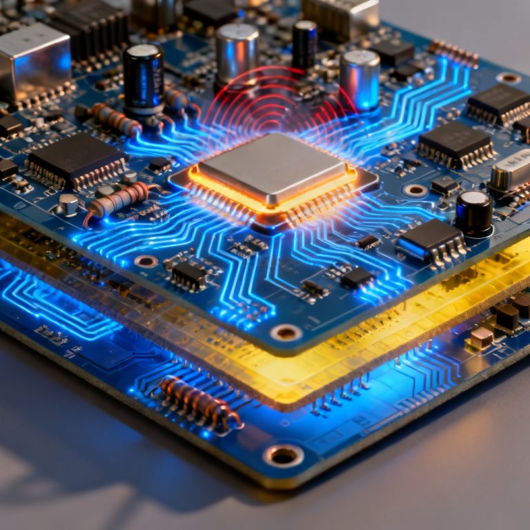
Power Integrity and Decoupling: Inductance is the enemy of fast switching. When a digital IC switches, it demands a rapid current spike. Inductance of the power supply path creates voltage drop (V = L × dI/dt), causing power supply noise or ground bounce. Place decoupling capacitors as close as possible to IC power pins, using low-ESL capacitors (0402 or 0201 packages) and multiple vias in parallel. A standard via (diameter 0.3 mm, length 1.6 mm) has about 0.5–1 nH inductance; multiple vias reduce effective inductance by roughly the square root of the number of vias.
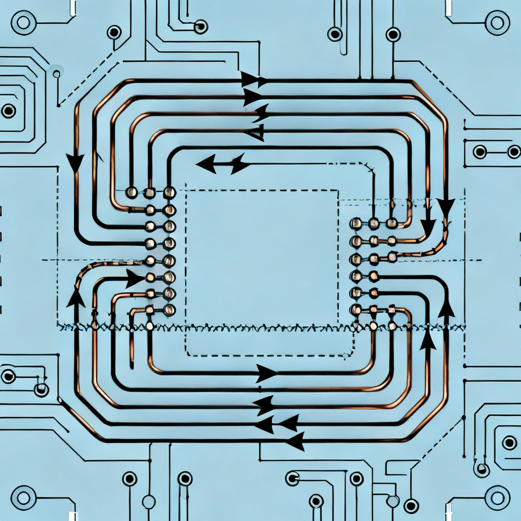
Signal Integrity and Return Path Discontinuities: For high-speed signals, the signal trace and its return path form a loop. Any discontinuity (e.g., slot in ground plane, layer change) increases loop area and inductance, causing increased crosstalk, signal reflections, and common-mode radiation (EMI). Provide a continuous, low-inductance return path directly under the signal trace using ground planes, avoid splits in ground planes under high-speed traces, and use ground vias when transitioning between layers.
Via Inductance and Stub Effects: A via stub acts as a transmission line stub, creating capacitive and inductive discontinuities. Above ~5 GHz, stub resonances cause significant signal loss and reflections. Back-drilling removes unused via stubs to reduce inductance. Smaller vias (microvias, laser-drilled, 0.1 mm diameter) have lower inductance but higher resistance.
Inductance in Power Electronics: In DC-DC converters, parasitic inductance in PCB layout (e.g., input capacitor to switch node loop) causes high-frequency ringing, EMI, and efficiency loss. Keep the high-current loop as small as possible using a solid ground plane and multiple vias.
3.4 Inductance Calculation and Simulation
For precise calculations, use field solvers (Ansys Q3D, HyperLynx, FastHenry). For quick estimation: trace inductance is approximately 1 nH per mm of trace length (10-mil wide trace over ground plane); via inductance is approximately 0.5–1 nH per via (length 1.6 mm); loop inductance is minimized by reducing current loop area (width × height).
3.5 B2B Specification for Inductance Control
Specify layer stack-up with continuous ground planes (no splits) under high-speed layers, via diameter and plating thickness (consider microvias and back-drilling for high-speed), and material selection—low-Dk materials also have lower dielectric losses, though inductance is primarily geometry-driven.
4. Interplay and Practical Optimization of R, C, and L
4.1 Impedance (Z) – The Unified Parameter
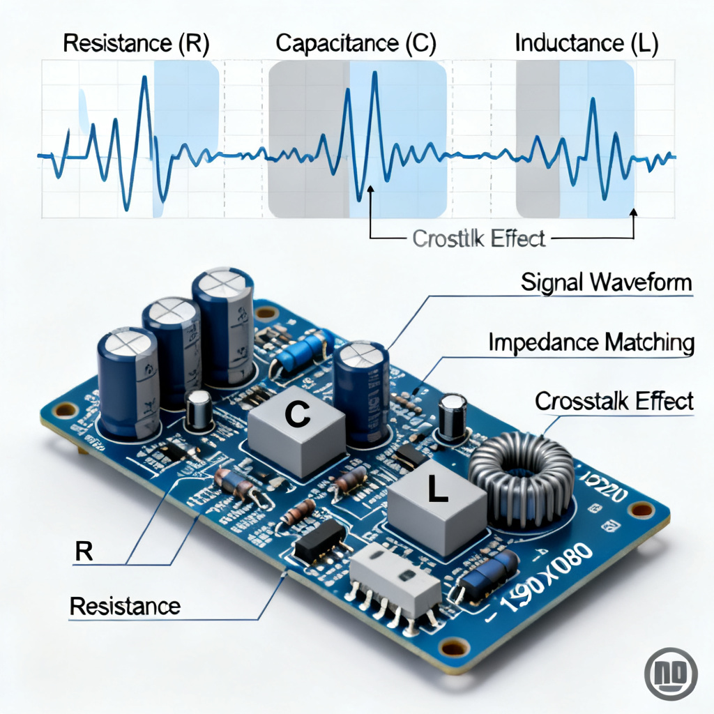
In AC circuits, the combined effect of R, C, and L is impedance (Z). For a series RLC circuit: Z = √(R² + (XL – XC)²), where XL = ωL (inductive reactance) and XC = 1/(ωC) (capacitive reactance). At the resonant frequency (f₀ = 1/(2π√(LC))), XL = XC, and impedance is purely resistive.
4.2 Signal Integrity: The RLC Trade-off
- Rise Time Degradation: High resistance and capacitance form an RC time constant (τ = RC) that slows signal edges.
- Ringing and Overshoot: Inductance and capacitance cause LC resonance, leading to ringing. Add series resistors (e.g., 22–33 Ω) to dampen resonance.
- Crosstalk: Mutual capacitance and mutual inductance between adjacent traces cause crosstalk. Use shielding, spacing, and orthogonal routing.
4.3 Power Integrity: The RLC Balance
- Low Resistance: Minimize IR drop and I²R loss.
- Low Inductance: Minimize dI/dt voltage spikes.
- High Distributed Capacitance: Provide high-frequency decoupling.
4.4 Electromagnetic Interference (EMI)
- Differential Mode EMI: Caused by signal loop. Minimize loop area (reduce inductance) to lower radiation.
- Common Mode EMI: Caused by parasitic capacitance to ground and unbalanced currents. Use common-mode chokes and proper grounding.
4.5 Thermal Management
- Resistance generates heat (I²R). Use thick copper and wide traces.
- Capacitance and inductance do not dissipate power ideally, but parasitic effects can cause heating due to dielectric losses (tan δ) and core losses in inductors.
5. Advanced Topics and Best Practices
5.1 Frequency-Dependent Behavior
- Resistance: Increases with frequency due to skin effect and proximity effect.
- Capacitance: Decreases slightly at very high frequencies due to dielectric relaxation; dielectric constant (Dk) also decreases with frequency.
- Inductance: Remains relatively constant with frequency, but mutual inductance effects become more pronounced.
5.2 Modeling and Simulation
Use SPICE or IBIS models for component-level simulation. For PCB-level analysis, use 3D electromagnetic field solvers (HFSS, CST) for accurate RLC extraction at high frequencies.
5.3 Design for Manufacturing (DFM)
- Resistance: Ensure trace widths are within manufacturer’s capabilities (minimum width/spacing).
- Capacitance: Specify dielectric thickness and Dk tolerance to ensure impedance control.
- Inductance: Avoid unnecessary vias and long loops. Use via-in-pad for high-speed BGA packages.
5.4 B2B Procurement Checklist
When ordering PCBs with tight RLC requirements, provide: stack-up drawing with material types, thicknesses, and Dk values; impedance control requirements (e.g., 50 Ω ± 10% for specific layers); copper weight and trace width/space rules; via specifications (diameter, plating, back-drilling required); surface finish (ENIG for gold contacts, HASL for general purpose); and testing requirements (e.g., TDR for impedance, 4-wire Kelvin for low resistance).
Conclusion
Mastering Electrical Parameters – Resistance, Capacitance, Inductance is essential for any B2B PCB engineer or procurement professional. These three parameters interact dynamically to determine signal integrity, power delivery, EMI performance, and thermal behavior. By understanding their physics, practical implications, and mitigation strategies, you can design and specify PCBs that meet demanding requirements—from high-speed digital to high-frequency RF and power electronics. Partner with a manufacturer that understands these fundamentals, provide clear specifications, use simulation tools, and always consider frequency-dependent behavior for reliable, high-performance boards.
FAQ: Electrical Parameters – Resistance, Capacitance, Inductance
What are the three fundamental electrical parameters in PCB design?
How does skin effect impact resistance in high-frequency PCBs?
What is the role of capacitance in power distribution networks?
How can I minimize parasitic inductance in PCB layout?
Our PCB Manufacturing Advantage: RLC Optimization
Unlike generic manufacturers, our advanced fabrication processes ensure precise control of Electrical Parameters – Resistance, Capacitance, Inductance. We offer thick copper options (up to 10 oz) for low-resistance power paths, low-loss high-frequency laminates (Rogers, Isola, Taconic) for stable capacitance, and microvia/back-drilling capabilities to minimize parasitic inductance. Our engineering team provides free stack-up design and impedance simulation, ensuring your boards meet stringent signal integrity requirements. Choose us for reliable, high-performance PCBs tailored to your exact RLC specifications.