Lamination Process for Multilayer PCBs
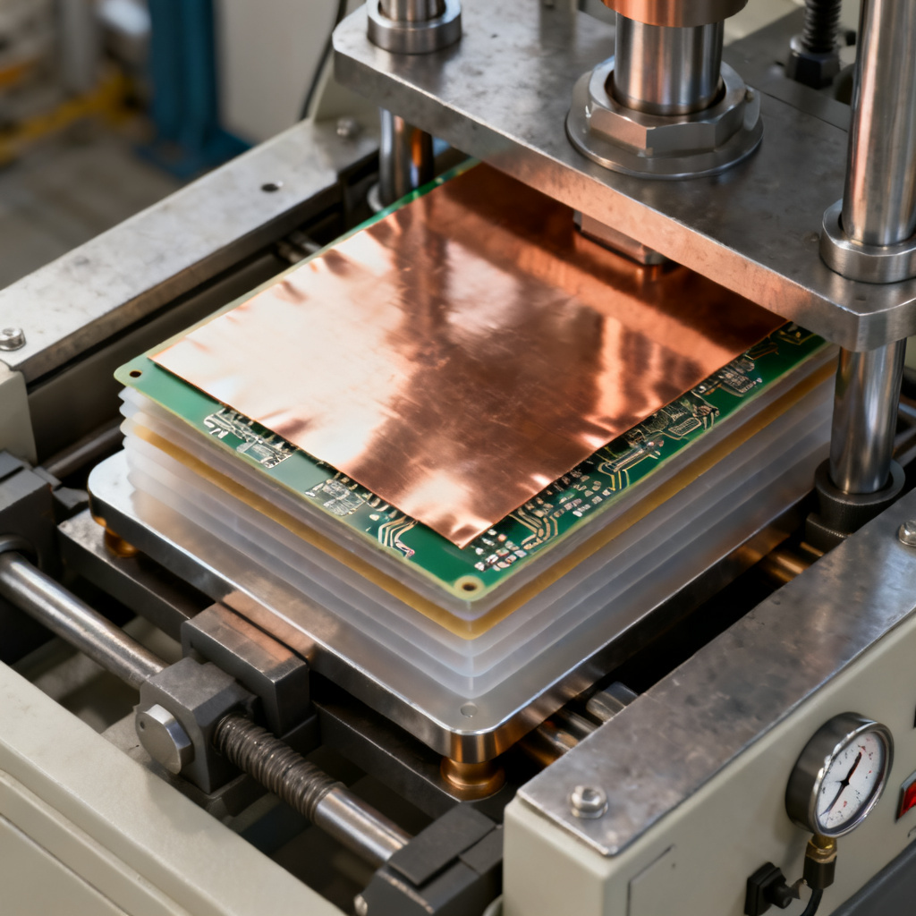
The lamination process for multilayer PCBs is the critical step where individual layers of copper-clad laminate and prepreg are bonded into a single, robust board under controlled heat and pressure. For B2B buyers designing high-speed digital, RF, or HDI boards, mastering this process ensures reliable, defect-free production.
- Material Preparation
- Lay-Up Process
- Lamination Cycle
- Post-Lamination Processing
- Quality Control
- Advanced Considerations
- FAQ
1. Material Preparation for Lamination Process for Multilayer PCBs
Before the lamination process for multilayer PCBs begins, all materials must be conditioned to prevent moisture-related defects.
1.1 Inner Layer Core Preparation
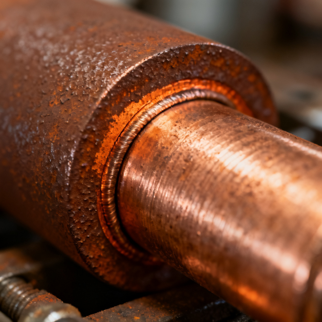
Inner layer cores undergo brown oxide or alternative oxide treatment to create a micro-roughened surface for enhanced adhesion. Cores are cleaned and baked at 120°C–150°C for 1–2 hours to remove moisture.
1.2 Prepreg Selection and Storage
Prepreg is chosen based on dielectric constant (Dk) and flow characteristics. Standard types include FR-4 (7628, 2116, 1080) and high-speed materials. Storage must be below 50% RH, with pre-drying at 100°C–120°C for 30–60 minutes.
1.3 Copper Foil
Standard electrodeposited (ED) copper foil or rolled-annealed (RA) foil is used. Low-profile copper (VLP or RTF) reduces signal loss for high-frequency designs.
2. Lay-Up Process in Lamination Process for Multilayer PCBs
The lay-up determines alignment accuracy and final thickness.
2.1 Stacking Sequence
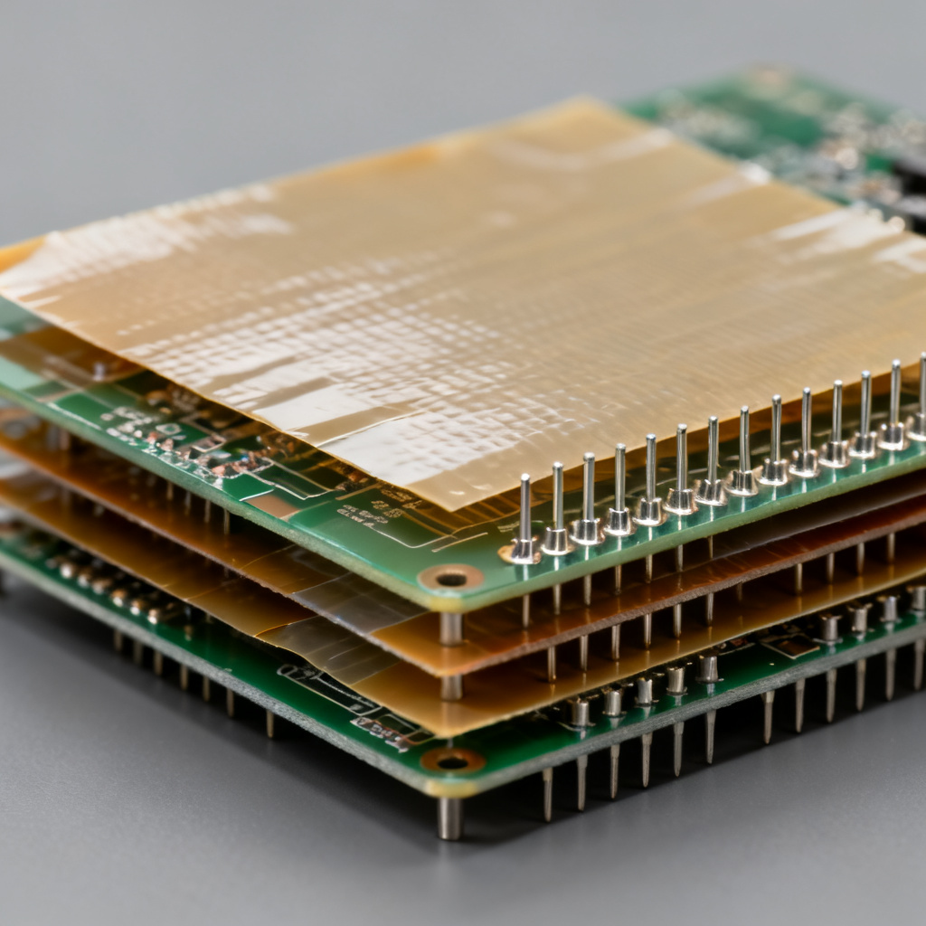
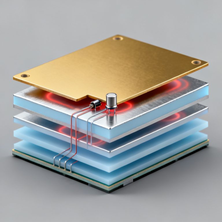
For a 4-layer board: copper foil → prepreg → inner layer core → prepreg → copper foil. Symmetrical stacks prevent warpage.
2.2 Alignment Systems
Tooling pins or optical alignment systems achieve ±25 µm registration.
2.3 Release Sheets and Cushioning
Release film (PTFE or polyimide) and cushion paper equalize pressure and absorb resin bleed.
2.4 Vacuum Sealing
Vacuum at 0.1–0.5 mbar for 15–30 minutes removes air pockets.
3. Lamination Cycle: Heat, Pressure, and Time
The press applies a controlled cycle to cure resin and bond layers.
3.1 Press Types
Hydraulic press (up to 400 psi), vacuum press, or autoclave.
3.2 Temperature Profile
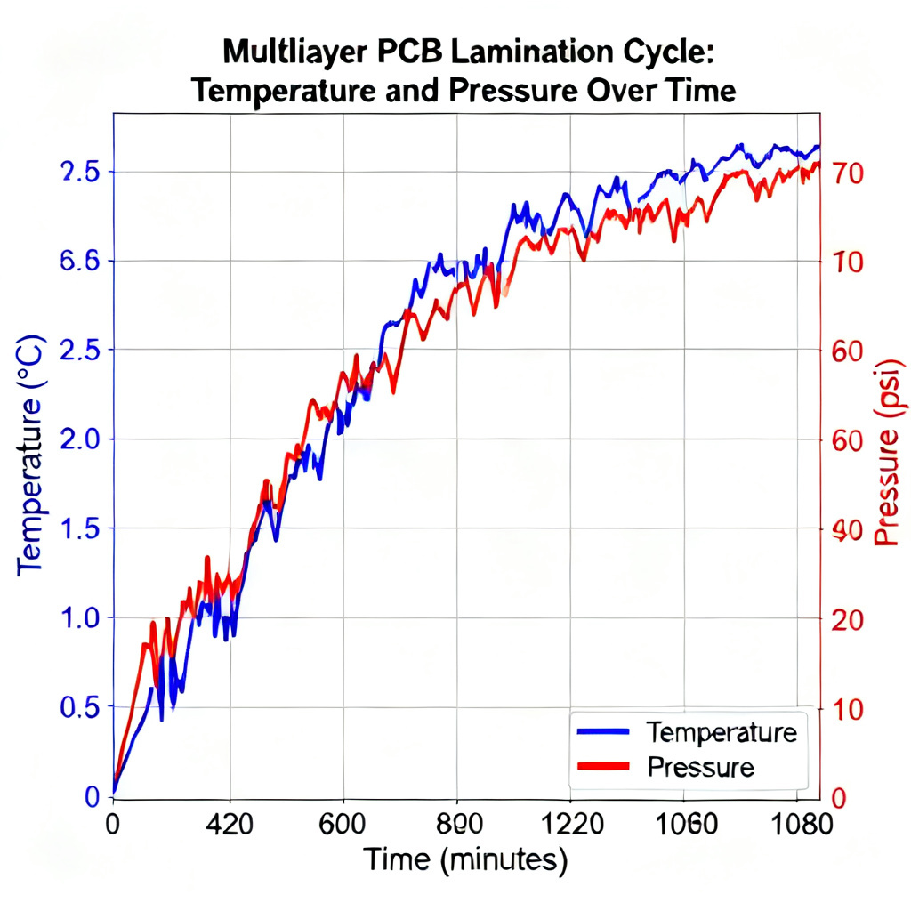
Ramp-up at 2°C–5°C per minute to 170°C–190°C (FR-4). Dwell time 60–120 minutes at peak.
3.3 Pressure Profile
Initial low pressure (50–100 psi) for resin flow, then full pressure (200–400 psi) after gel point.
3.4 Resin Flow Control
High-resin-content prepreg (e.g., 1080 with ~65% resin) fills gaps. Bleed-out is monitored via test coupons.
4. Post-Lamination Processing
After the cycle, boards undergo cooling, de-paneling, X-ray registration check, thickness measurement, and visual inspection.
5. Quality Control in Lamination Process for Multilayer PCBs
Rigorous QC ensures IPC-6012 compliance.
5.1 Common Defects
Delamination, voids, warpage, and resin starvation are prevented by proper baking, vacuum, and symmetrical design.
5.2 Destructive Testing
Microsectioning, peel strength test (min 6 lb/in), solder float test (288°C for 10 seconds).
5.3 Non-Destructive Testing
Automated optical inspection (AOI) and ultrasonic scanning (C-SAM) detect internal defects.
6. Advanced Considerations
6.1 High-Tg and High-Speed Materials
Materials like Isola 370HR or Rogers 4350B require peak temperatures of 200°C–220°C and longer dwell times.
6.2 HDI Lamination
Sequential lamination with multiple cycles for microvias.
6.3 Rigid-Flex Lamination
Reduced pressure (100–200 psi) and special bonding film protect flex layers.
| Parameter | Standard Value | High-Performance Value |
|---|---|---|
| Peak Temperature | 170°C–190°C (FR-4) | 200°C–220°C (High-Tg) |
| Pressure | 200–400 psi | 100–200 psi (Rigid-Flex) |
| Dwell Time | 60–120 minutes | 90–120 minutes |
| Registration Tolerance | ±50 µm | ±25 µm (HDI) |
FAQ: Lamination Process for Multilayer PCBs
What is the lamination process for multilayer PCBs?
The lamination process for multilayer PCBs bonds inner layers, prepreg, and copper foil under heat and pressure to form a single board.
How does prepreg affect the lamination process for multilayer PCBs?
Prepreg resin content and flow characteristics determine dielectric thickness and void prevention.
What defects can occur in the lamination process for multilayer PCBs?
Common defects include delamination, voids, and warpage, prevented by proper material conditioning and vacuum.
Why is vacuum important in the lamination process for multilayer PCBs?
Vacuum removes air and volatiles, preventing voids and ensuring uniform bonding.
How is quality controlled in the lamination process for multilayer PCBs?
Through microsectioning, peel strength tests, solder float tests, AOI, and C-SAM.