HDI Manufacturing Microvia Fill and Lay up
HDI Manufacturing is essential for modern compact electronics, enabling high‑density interconnects through precise microvia formation, via filling, and layer lay‑up. This guide:”HDI Manufacturing Microvia Fill and Lay up” covers every critical process for reliable HDI PCB production.
HDI Manufacturing: Microvia Technology, Types, and Reliability
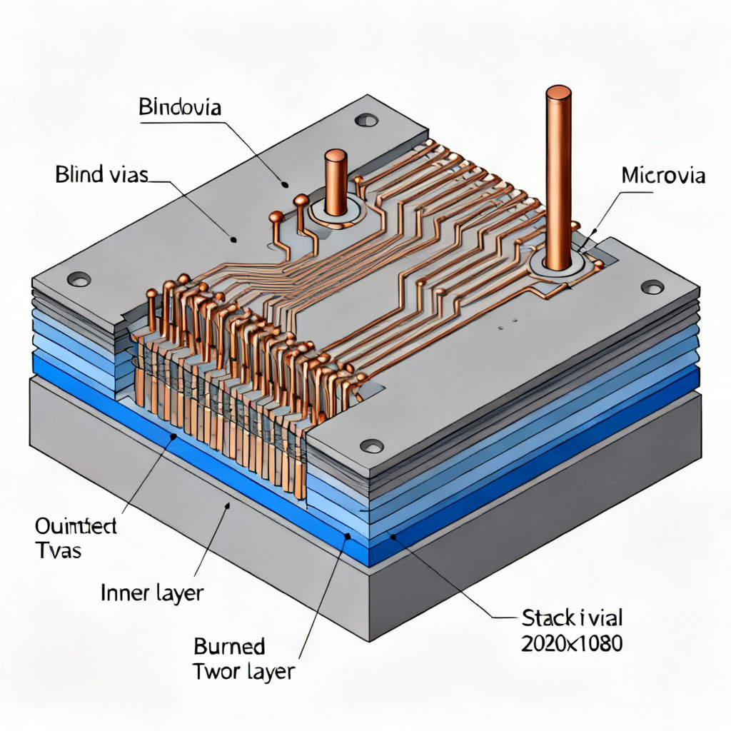
What Is a Microvia in HDI Manufacturing?
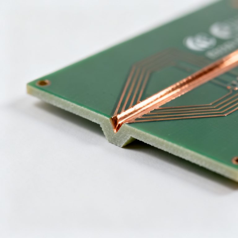
A microvia is a small blind or buried via with diameter ≤0.15 mm and aspect ratio ≤1:1, critical in HDI Manufacturing for routing between adjacent layers without consuming board space. Per IPC‑6012 and IPC‑6016, microvias are classified as Type I (blind), Type II (buried), and Type III (stacked/staggered).
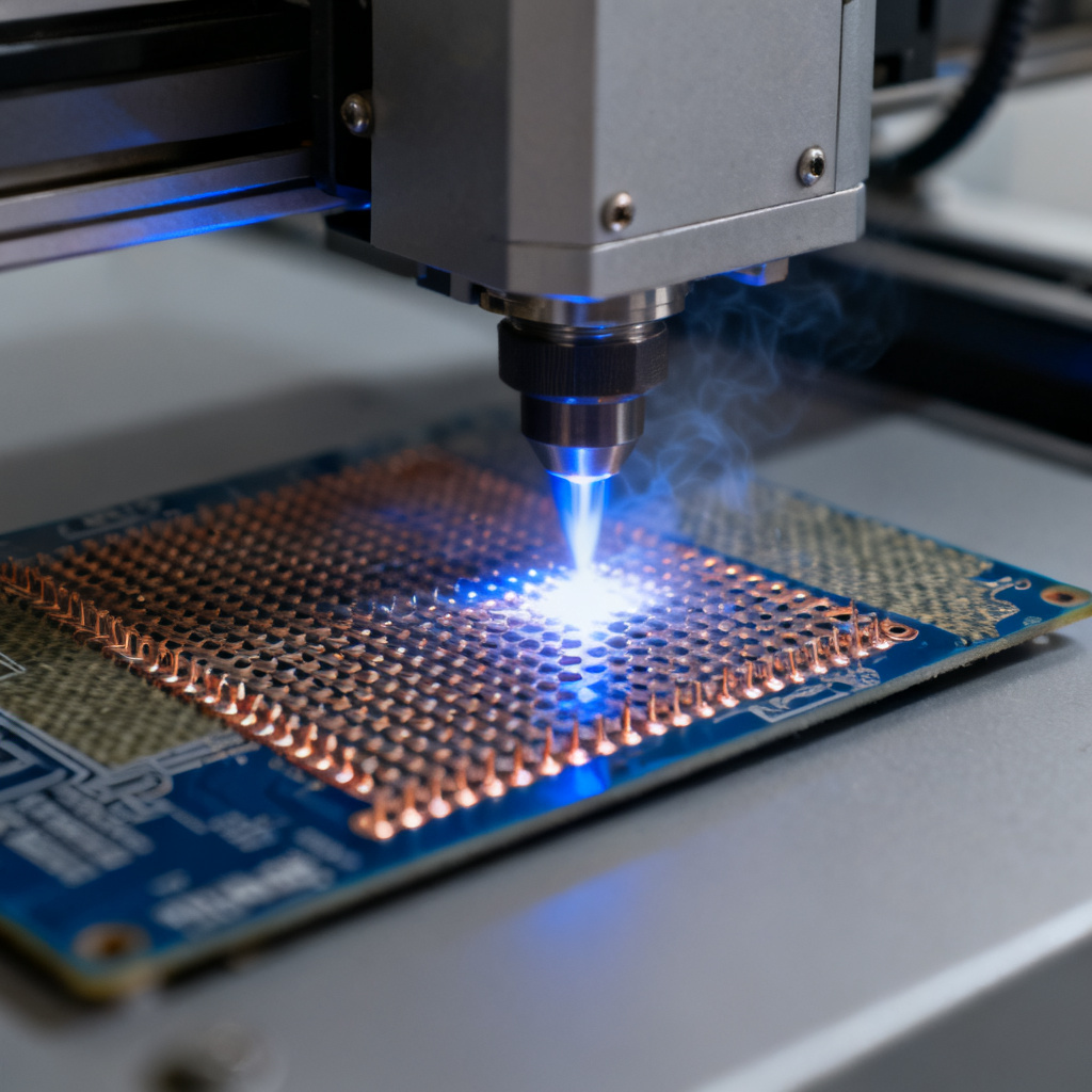
Formation Methods for HDI Manufacturing
Laser Drilling (CO₂ vs. UV/YAG): CO₂ lasers remove resin and glass in FR‑4; UV lasers offer finer control. Plasma Etching suits PTFE or LCP dielectrics. Photo‑Definable Dielectrics enable stacked vias via photolithography.
Aspect Ratio and Reliability Limits
Standard microvias: aspect ratio ≤0.75:1. High‑aspect microvias: up to 1:1. Reliability testing per IPC‑TM‑650 includes thermal cycling and micro‑section analysis.
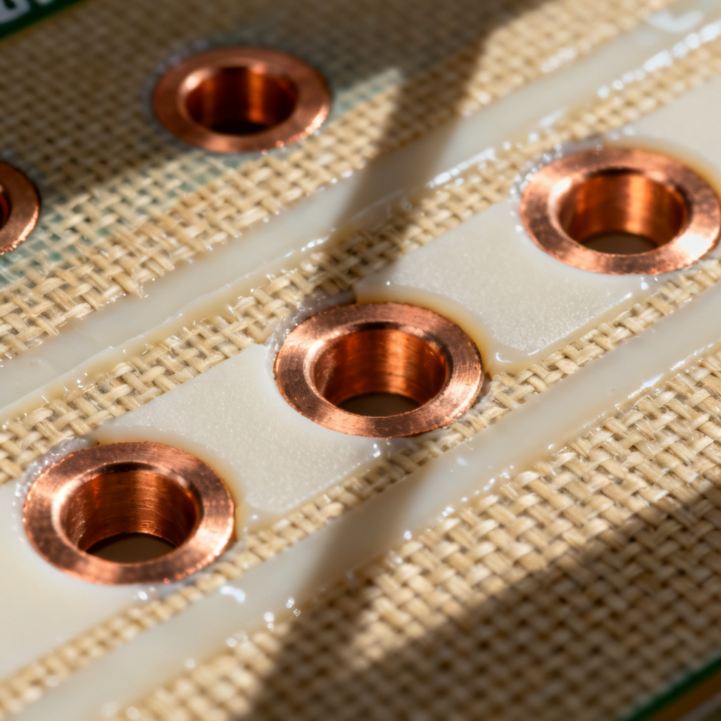
HDI Manufacturing: Via Filling – Materials, Processes, and Quality Control
Why Fill Vias in HDI Manufacturing?
Unfilled vias cause voiding, reduced current capacity, poor thermal management, and insufficient planarization. Filling ensures reliability in HDI Manufacturing.
Filling Materials for HDI Manufacturing
| Material | Advantages | Disadvantages |
|---|---|---|
| Copper‑filled | Excellent conductivity, thermal dissipation | Higher cost |
| Conductive epoxy | Good conductivity, lower temperature | Higher resistivity |
| Non‑conductive epoxy | Low cost, good planarization | No electrical connection |
| Solder‑filled | High‑current applications | Complex, limited |
Filling Process Steps for HDI Manufacturing
Desmear, electroless copper, electroplating, planarization, final plating. Quality metrics: void content ≤5%, surface flatness ≤0.025 mm, X‑ray inspection.
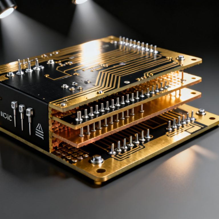
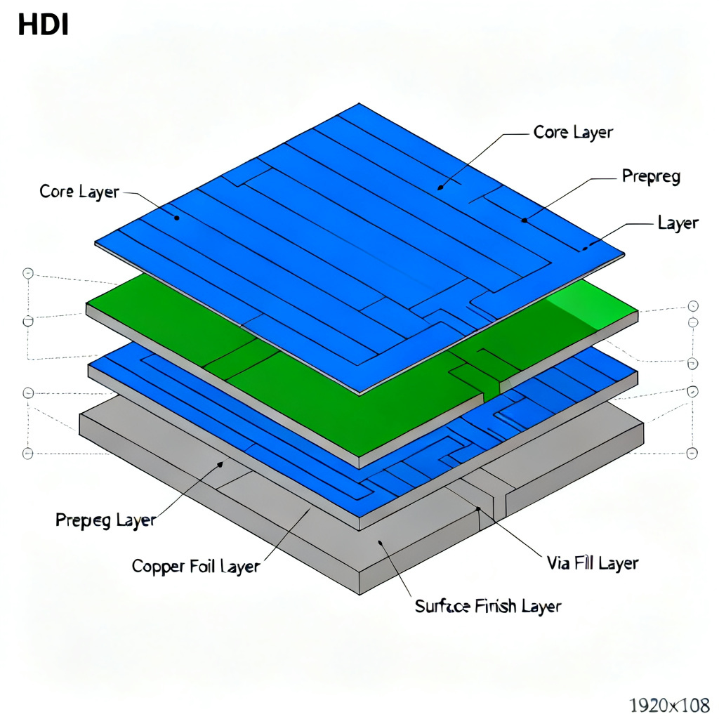
HDI Manufacturing: Layer Lay‑up – Stackup Design and Sequential Lamination
Sequential Lamination Process in HDI Manufacturing
Core layer preparation, first lamination, drilling and plating, second lamination, repeat up to 4–6 build‑up cycles.
Stackup Configurations for HDI Manufacturing
| Configuration | Layers | Typical Use |
|---|---|---|
| 1+N+1 | 1 build‑up per side | Simple HDI |
| 2+N+2 | 2 build‑ups per side | Mid‑range |
| 3+N+3 | 3 build‑ups per side | Advanced |
| Any‑layer HDI | All layers with microvias | Highest density |
Dielectric Materials and Critical Considerations
Standard FR‑4 prepreg, low‑loss materials (Rogers 4350B, Megtron 6), ultra‑thin dielectrics. Registration tolerance ±0.05 mm, symmetrical stackup for warpage control.
Design for Manufacturing (DFM) Best Practices in HDI Manufacturing
Microvia Design Rules
Minimum via diameter 0.1 mm, pad size via diameter + 0.15 mm, spacing ≥0.15 mm. Stacked vias limit to 3.
Fill Selection Guide
Blind vias: resin‑fill. Buried vias: copper‑fill if current >1A. Stacked vias: copper‑fill mandatory.
Testing and Quality Assurance in HDI Manufacturing
Electrical Testing
Flying probe, dedicated fixture, impedance testing via TDR.
Physical Inspection
Micro‑sectioning, X‑ray, Scanning Acoustic Microscopy.
Reliability Tests
Thermal cycling, solder shock, peel strength.
Common Challenges and Solutions in HDI Manufacturing
| Challenge | Cause | Solution |
|---|---|---|
| Microvia voiding | Incomplete desmear | Optimize plasma; use copper‑fill |
| Resin bleed‑out | High prepreg flow | Use low‑flow prepreg |
| Layer misregistration | Thermal expansion | X‑ray alignment |
| Warpage | Asymmetric stackup | Balance copper distribution |
| Via cracking | Thermal cycling stress | Limit stacked vias to 3 |
Why Choose a Trusted HDI Manufacturer?
IPC‑6012 Class 3 certification, in‑house laser drilling, AOI, 100% electrical testing, engineering support for DFM.
FAQ: HDI Manufacturing – Microvia, Fill, and Lay‑up
What is the most common microvia formation method in HDI Manufacturing?
Laser drilling (CO₂ or UV) is most common in HDI Manufacturing for precision and speed.
Why is via filling important in HDI Manufacturing?
Via filling prevents voiding, improves thermal management, and ensures planarization in HDI Manufacturing.
What is sequential lamination in HDI Manufacturing?
Sequential lamination builds up layers one by one, enabling high layer counts in HDI Manufacturing.
How do I choose between copper‑fill and epoxy‑fill in HDI Manufacturing?
Copper‑fill for conductivity and stacked vias; epoxy‑fill for cost‑effective blind vias in HDI Manufacturing.
What reliability tests are standard for HDI Manufacturing?
Thermal cycling, solder shock, and micro‑section analysis per IPC standards in HDI Manufacturing.