Complete PCB Manufacturing Process From Raw Material to Finished Board
The PCB manufacturing process transforms raw materials into precision-engineered boards that power modern electronics. This comprehensive guide:“Complete PCB Manufacturing Process From Raw Material to Finished Board” covers every step, from substrate selection to final inspection, providing B2B buyers and engineers with authoritative technical depth.
PCB Manufacturing Process: Raw Material Selection and Preparation
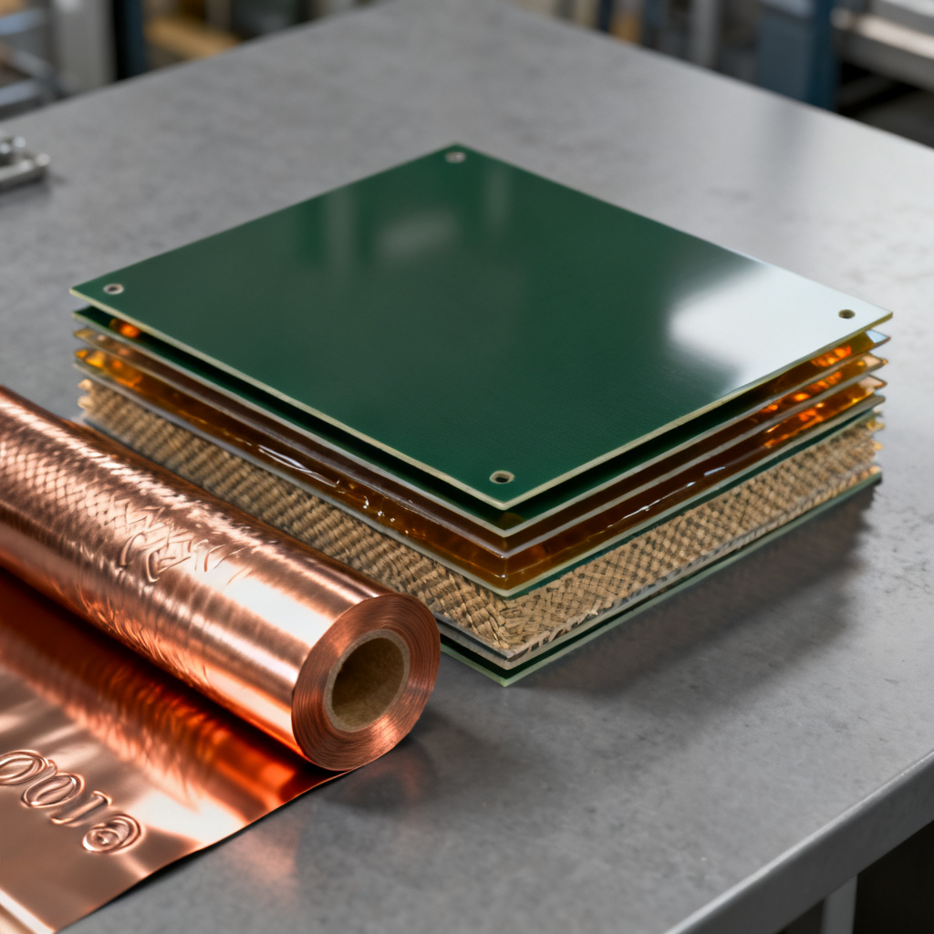
The foundation of any PCB manufacturing process is the copper-clad laminate (CCL). This material consists of a substrate (typically FR-4, a glass-reinforced epoxy) bonded with a thin layer of copper foil on one or both sides.
Key Raw Materials for PCB Manufacturing Process
- Substrate: FR-4 is standard for flame retardancy, mechanical strength, and electrical insulation. Other materials include high-Tg FR-4, polyimide (for flex), and Rogers (for high-frequency).
- Copper foil: Typically electrodeposited (ED) or rolled-annealed (RA). Thickness ranges from 0.5 oz/ft² to 3 oz/ft² or more.
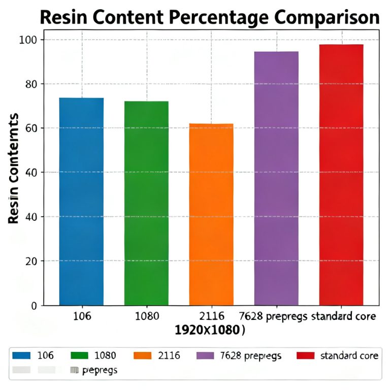
- Prepreg (pre-impregnated bonding sheets): B-stage epoxy resin used to bond layers in multilayer boards.
Pre-processing Steps in PCB Manufacturing Process
- Incoming inspection: Verify thickness, copper weight, and dielectric constant.
- Cutting to panel size: Raw panels are cut to standard production sizes (e.g., 18″ x 24″ or 20″ x 24″) using shear or saw.
- Cleaning: Panels are cleaned to remove dust, grease, or oxidation, ensuring proper adhesion.
Why this matters in PCB manufacturing process: Quality raw materials directly impact board reliability, impedance control, and thermal performance. Reputable manufacturers source from certified suppliers (e.g., Isola, Panasonic, Rogers).
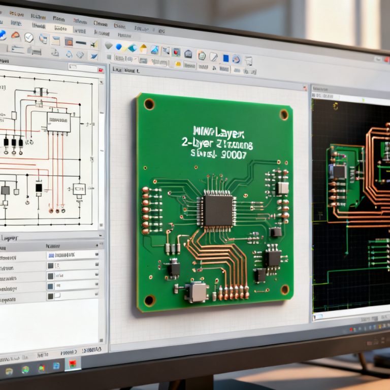
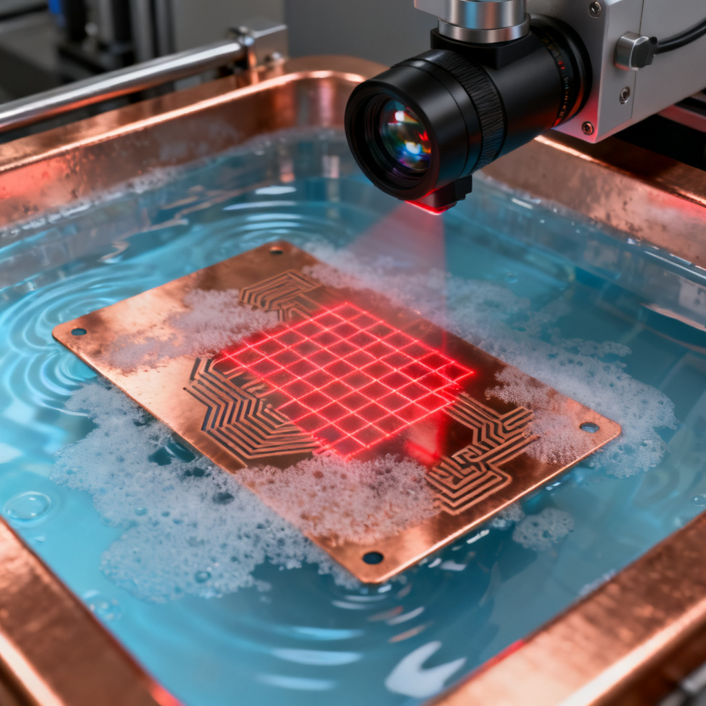
PCB Manufacturing Process: Inner Layer Imaging and Etching
For multilayer boards, the inner layers are processed first. This step transfers the circuit pattern onto the copper-clad laminate.
Process Flow in PCB Manufacturing Process
- Cleaning and lamination of dry film: A photosensitive dry film (photoresist) is laminated onto the clean copper surface using heat and pressure.
- Exposure: The panel is aligned with a phototool (film) or exposed using a direct imaging (LDI) laser system. UV light hardens the photoresist in the desired circuit pattern.
- Development: The unexposed (soft) photoresist is washed away in a developer solution (sodium carbonate), revealing the copper to be etched.
- Etching: The exposed copper is removed using a chemical etchant (typically cupric chloride or ferric chloride). The hardened photoresist protects the copper traces.
- Strip: The remaining photoresist is stripped off using a strong alkaline solution (e.g., sodium hydroxide), leaving the copper circuit pattern.
- AOI (Automated Optical Inspection): The etched inner layers are scanned by high-resolution cameras to detect opens, shorts, or defects before lamination.
Advanced note: LDI (Laser Direct Imaging) eliminates phototools, offering higher resolution and faster turnaround for complex designs.
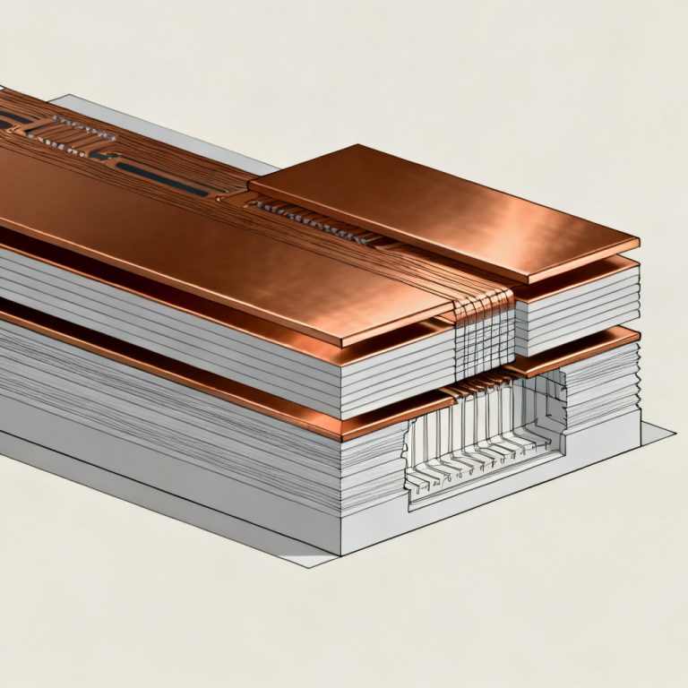
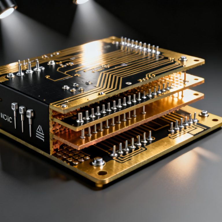
PCB Manufacturing Process: Layer Lamination (Pressing)
This step bonds all inner layers together with prepreg to form a single, solid multilayer board.
Process Steps in PCB Manufacturing Process
- Oxide treatment: Inner layer copper surfaces are chemically treated (black oxide or brown oxide) to enhance adhesion with prepreg.
- Stack-up: The layers are stacked in a precise order: outer copper foil, prepreg sheets, inner layers, more prepreg, and bottom foil. Each layer is aligned using tooling holes or an optical registration system.
- Lamination: The stack is placed in a hydraulic press under high temperature (170–190°C) and pressure (300–500 psi) for 1–2 hours. The prepreg melts and flows, bonding all layers.
- Cooling: The board is cooled under pressure to prevent warping.
- X-ray registration: After lamination, X-ray inspection verifies layer alignment.
Critical Parameters in PCB Manufacturing Process
- Temperature ramp rate
- Vacuum pressure (to eliminate voids)
- Resin flow control
Why this matters: Poor lamination can cause delamination, voids, or misregistration, leading to board failure.
PCB Manufacturing Process: Drilling
Drilling creates holes for component leads (through-holes) and vias (connections between layers). Precision is critical for multilayer alignment.
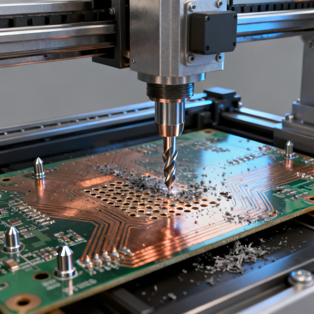
Process in PCB Manufacturing Process
- X-ray drill: A small X-ray target is drilled to locate inner layer targets.
- CNC drilling: High-speed CNC drilling machines (e.g., from Schmoll, Hitachi) use tungsten carbide or diamond-coated bits. Speeds up to 150,000 RPM.
- Hole sizes: Typically 0.2mm to 6.0mm. Smaller holes require laser drilling (UV or CO2).
- Back drilling: For high-speed designs, back drilling removes unused stub portions of plated through-holes.
Deburring: After drilling, panels are deburred to remove rough edges around holes.
Quality control: Hole position accuracy is checked using optical measurement.
PCB Manufacturing Process: Electroless Copper Plating (PTH)
Before plating, the board is non-conductive. Electroless copper plating deposits a thin layer of copper (0.5–1.0 microns) onto the hole walls, making them conductive for subsequent electroplating.
Process Steps in PCB Manufacturing Process
- Desmear: Plasma or chemical treatment removes resin smear from drilling, exposing inner layer copper rings inside holes.
- Catalyzing: Palladium-tin colloidal catalyst is applied to the hole walls to initiate copper deposition.
- Electroless copper: The board is immersed in a copper bath (formaldehyde-based or electroless copper) that deposits copper via chemical reduction.
- Rinse and dry.
Common issues: Poor desmear leads to voids in the hole wall, causing electrical opens.
PCB Manufacturing Process: Outer Layer Imaging and Etching
This is similar to inner layer imaging but applied to the outer copper layers.
Process in PCB Manufacturing Process
- Panel plating: A thin layer of copper is electroplated onto the entire panel (optional, often done after imaging).
- Dry film lamination: Photoresist is applied to both sides.
- Exposure and development: Circuit pattern is transferred.
- Pattern plating: Additional copper is electroplated onto the exposed areas (traces and pads) to build up thickness.
- Tin plating: A thin layer of tin (or tin-lead) is electroplated onto the copper traces as an etch resist.
- Strip and etch: The photoresist is stripped, and the exposed copper (not covered by tin) is etched away. The tin resist protects the traces.
- Tin strip: Finally, the tin is stripped off, leaving the finished outer copper pattern.
Alternative process: Some manufacturers use tenting (covering pads with dry film) or direct metalization for finer line widths.
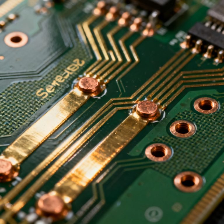
PCB Manufacturing Process: Solder Mask Application
Solder mask is a protective polymer layer that prevents solder bridges, protects copper from oxidation, and provides electrical insulation.
Types of Solder Mask in PCB Manufacturing Process
- Liquid photoimageable (LPI) solder mask: Most common. Applied by curtain coating, screen printing, or electrostatic spray.
- Dry film solder mask: Used for fine-pitch or high-reliability boards.
- Color: Green is standard, but red, blue, black, white, and yellow are available.
Process in PCB Manufacturing Process
- Cleaning: Board is cleaned and dried.
- Application: LPI solder mask is sprayed or curtain-coated onto both sides.
- Pre-bake: The board is heated to remove solvent (65–80°C).
- Exposure: UV light is shone through a phototool to harden the mask in areas where it should remain (over traces and planes).
- Development: Unexposed mask is washed away, opening pads and vias.
- Final cure: The board is baked at 140–150°C for 30–60 minutes to fully cure the mask.
Quality check: Solder mask registration is critical to avoid exposing adjacent pads.
PCB Manufacturing Process: Surface Finish
Surface finish protects exposed copper pads and ensures solderability. The choice of finish depends on application, cost, and reliability requirements.
Common Finishes in PCB Manufacturing Process
| Surface Finish | Key Characteristics | Best For |
|---|---|---|
| HASL (Hot Air Solder Leveling) | Leaded or lead-free; cheap but not flat | General purpose, low-cost applications |
| ENIG (Electroless Nickel Immersion Gold) | Flat, durable, excellent for fine-pitch and wire bonding | High-density, fine-pitch, and high-reliability boards |
| OSP (Organic Solderability Preservative) | Environmentally friendly but short shelf life | Low-cost, lead-free, and short-term storage |
| Immersion Silver | Good for high-frequency but prone to tarnishing | RF/microwave and high-speed digital |
| Immersion Tin | Flat but sensitive to handling | Fine-pitch and press-fit applications |
| ENEPIG (Electroless Nickel Electroless Palladium Immersion Gold) | For high-reliability and multiple reflow cycles | Advanced packaging, automotive, aerospace |
Process Example: ENIG in PCB Manufacturing Process
- Acid cleaning and micro-etch.
- Palladium activation.
- Electroless nickel deposition (3–6 microns).
- Immersion gold deposition (0.05–0.15 microns).
Why it matters: The finish affects assembly yield, reliability, and cost.
PCB Manufacturing Process: Electrical Testing
Every PCB must be tested for electrical continuity and isolation to ensure it functions as designed.
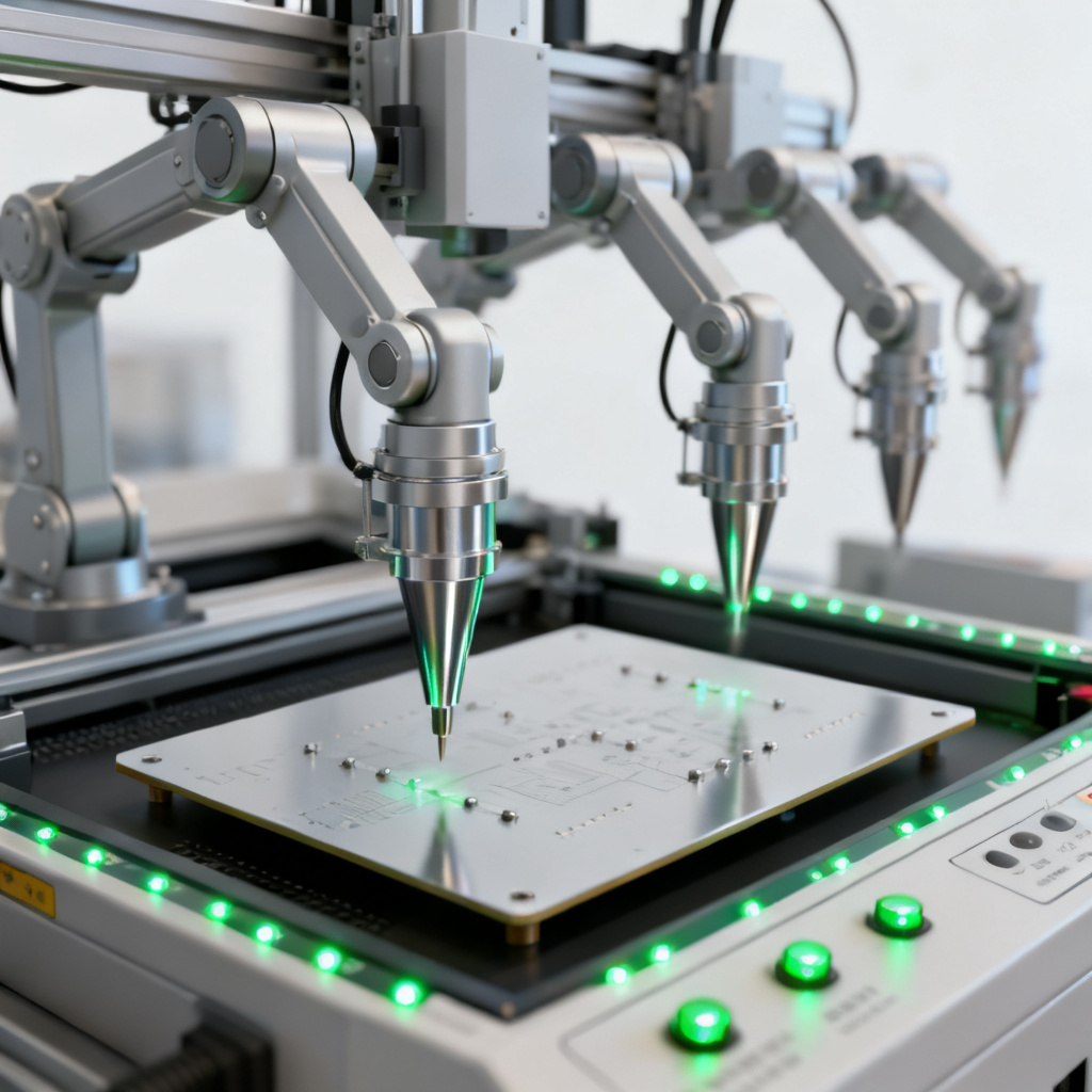
Testing Methods in PCB Manufacturing Process
- Flying probe testing: Uses moving probes to test nets. Ideal for prototypes and low volume.
- Fixture-based testing (bed of nails): Uses a custom fixture with pogo pins. High speed for mass production.
- Capacitive testing: Non-contact method for detecting opens/shorts in inner layers.
Parameters Tested in PCB Manufacturing Process
- Continuity (all nets connected)
- Isolation (no shorts between nets)
- Resistance and capacitance (optional)
- Impedance control (for high-speed designs)
Acceptance criteria: IPC-600 Class 2 (standard) or Class 3 (high-reliability).
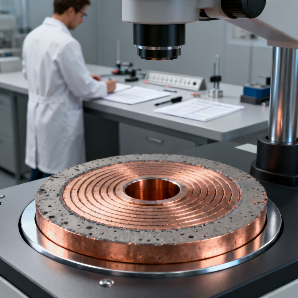
PCB Manufacturing Process: Final Inspection and Quality Assurance
Before shipping, boards undergo a final quality check.
Inspection Steps in PCB Manufacturing Process
- Visual inspection: Check for scratches, pinholes, solder mask defects, registration errors.
- Dimensional measurement: Verify board outline, hole sizes, and pad diameters.
- Solderability test: Dip a sample board in molten solder to check wetting.
- Microsection analysis: Cut a cross-section of a coupon (test piece) to inspect plating thickness, hole wall quality, and layer alignment under a microscope.
- Impedance coupon test: Measure actual impedance on a dedicated test coupon.
- Cleanliness test: Ionic contamination test (e.g., IPC-TM-650) to ensure no residual flux or chemicals.
Packaging: Boards are vacuum-sealed with desiccant and humidity indicator cards to prevent oxidation during shipping.
Comparison: Our PCB Manufacturing Process vs. Industry Standards
Our PCB manufacturing process adheres to IPC-6012 Class 2 and Class 3 standards, with additional quality checks such as 100% electrical testing and microsection analysis on every production batch. Unlike many competitors who outsource final inspection, we perform all testing in-house, ensuring faster feedback and higher consistency. We also offer free DFM review to identify potential issues before production, reducing costly rework.
Industry Terminology Explained
- Impedance Control: Managing the characteristic impedance of traces to match design specifications, critical for high-speed signals.
- Microvia: A small via (typically ≤0.15mm) used in HDI boards for high-density interconnects.
- Backdrilling: Removing unused via stubs to reduce signal reflection in high-speed designs.
- Prepreg: Bonding material used between layers in multilayer PCB manufacturing process.
FAQ: PCB Manufacturing Process
What is the first step in the PCB manufacturing process?
The first step in the PCB manufacturing process is raw material selection and preparation, where copper-clad laminate (CCL) is inspected and cut to panel size.
How long does the PCB manufacturing process take?
A standard PCB manufacturing process for a 4-layer board typically takes 5-10 business days, depending on complexity and quantity. Advanced boards (e.g., 20+ layers or HDI) may require 15-20 days.
What is the difference between HASL and ENIG in the PCB manufacturing process?
HASL (Hot Air Solder Leveling) is a cheaper, less flat surface finish, while ENIG (Electroless Nickel Immersion Gold) offers a flat, durable surface ideal for fine-pitch components and high-reliability applications in the PCB manufacturing process.
Why is impedance control important in the PCB manufacturing process?
Impedance control ensures that signal traces have consistent characteristic impedance, preventing signal reflection and degradation in high-speed digital and RF circuits. This is a critical quality parameter in the PCB manufacturing process.
What is the most common material used in the PCB manufacturing process?
FR-4 (glass-reinforced epoxy) is the most common substrate material due to its balance of cost, mechanical strength, and electrical insulation properties in the PCB manufacturing process.
{ “@context”: “https://schema.org”, “@graph”: [ { “@type”: “BreadcrumbList”, “@id”: “https://pcbtypes.com/complete-pcb-manufacturing-process-from-raw-material-to-finished-board.html#breadcrumb”, “itemListElement”: [ { “@type”: “ListItem”, “position”: 1, “name”: “Home”, “item”: “https://pcbtypes.com/” }, { “@type”: “ListItem”, “position”: 2, “name”: “PCB Manufacturing Processes”, “item”: “https://pcbtypes.com/category/pcb-manufacturing-processes” }, { “@type”: “ListItem”, “position”: 3, “name”: “Complete PCB Manufacturing Process From Raw Material to Finished Board”, “item”: “https://pcbtypes.com/complete-pcb-manufacturing-process-from-raw-material-to-finished-board.html” } ] }, { “@type”: “TechArticle”, “@id”: “https://pcbtypes.com/complete-pcb-manufacturing-process-from-raw-material-to-finished-board.html#article”, “isPartOf”: { “@type”: “WebPage”, “@id”: “https://pcbtypes.com/complete-pcb-manufacturing-process-from-raw-material-to-finished-board.html” }, “headline”: “Complete PCB Manufacturing Process From Raw Material to Finished Board”, “description”: “Comprehensive B2B engineering guide covering the complete PCB manufacturing process, including raw material selection, lamination, drilling, plating, solder mask, surface finish, and electrical testing.”, “inLanguage”: “en-US”, “mainEntityOfPage”: “https://pcbtypes.com/complete-pcb-manufacturing-process-from-raw-material-to-finished-board.html”, “datePublished”: “2026-06-11T15:13:00+00:00”, “dateModified”: “2026-06-11T15:13:00+00:00”, “author”: { “@type”: “Organization”, “name”: “Sensormass”, “url”: “https://pcbtypes.com/” }, “publisher”: { “@type”: “Organization”, “name”: “Sensormass”, “logo”: { “@type”: “ImageObject”, “url”: “https://pcbtypes.com/wp-content/uploads/logo.png” } }, “image”: { “@type”: “ImageObject”, “url”: “https://pcbtypes.com/wp-content/uploads/pcb-cnc-drilling-machine-high-speed.jpg”, “caption”: “Complete PCB manufacturing process from raw material to finished board for global B2B electronics sourcing.” }, “dependencies”: “FR-4, Copper Foil, Prepreg”, “proficiencyLevel”: “Expert” }, { “@type”: “FAQPage”, “@id”: “https://pcbtypes.com/complete-pcb-manufacturing-process-from-raw-material-to-finished-board.html#faq”, “mainEntity”: [ { “@type”: “Question”, “name”: “What is the first step in the PCB manufacturing process?”, “acceptedAnswer”: { “@type”: “Answer”, “text”: “The first step in the PCB manufacturing process is raw material selection and preparation, where copper-clad laminate (CCL) is inspected and cut to panel size.” } }, { “@type”: “Question”, “name”: “How long does the PCB manufacturing process take?”, “acceptedAnswer”: { “@type”: “Answer”, “text”: “A standard PCB manufacturing process for a 4-layer board typically takes 5-10 business days, depending on complexity and quantity. Advanced boards (e.g., 20+ layers or HDI) may require 15-20 days.” } }, { “@type”: “Question”, “name”: “What is the difference between HASL and ENIG in the PCB manufacturing process?”, “acceptedAnswer”: { “@type”: “Answer”, “text”: “HASL (Hot Air Solder Leveling) is a cheaper, less flat surface finish, while ENIG (Electroless Nickel Immersion Gold) offers a flat, durable surface ideal for fine-pitch components and high-reliability applications in the PCB manufacturing process.” } }, { “@type”: “Question”, “name”: “Why is impedance control important in the PCB manufacturing process?”, “acceptedAnswer”: { “@type”: “Answer”, “text”: “Impedance control ensures that signal traces have consistent characteristic impedance, preventing signal reflection and degradation in high-speed digital and RF circuits. This is a critical quality parameter in the PCB manufacturing process.” } }, { “@type”: “Question”, “name”: “What is the most common material used in the PCB manufacturing process?”, “acceptedAnswer”: { “@type”: “Answer”, “text”: “FR-4 (glass-reinforced epoxy) is the most common substrate material due to its balance of cost, mechanical strength, and electrical insulation properties in the PCB manufacturing process.” } } ] } ] }