PCB Type Comparison Rigid vs Flex HDI vs Standard
This comprehensive PCB Type Comparison Rigid vs Flex HDI vs Standard manual is about advanced board selection rules for hardware engineers and procurement managers. Choosing the correct circuit board substrate is critical for product performance, reliability, and total cost of ownership. This guide helps technical professionals make an informed decision for their next high-speed or high-density project.
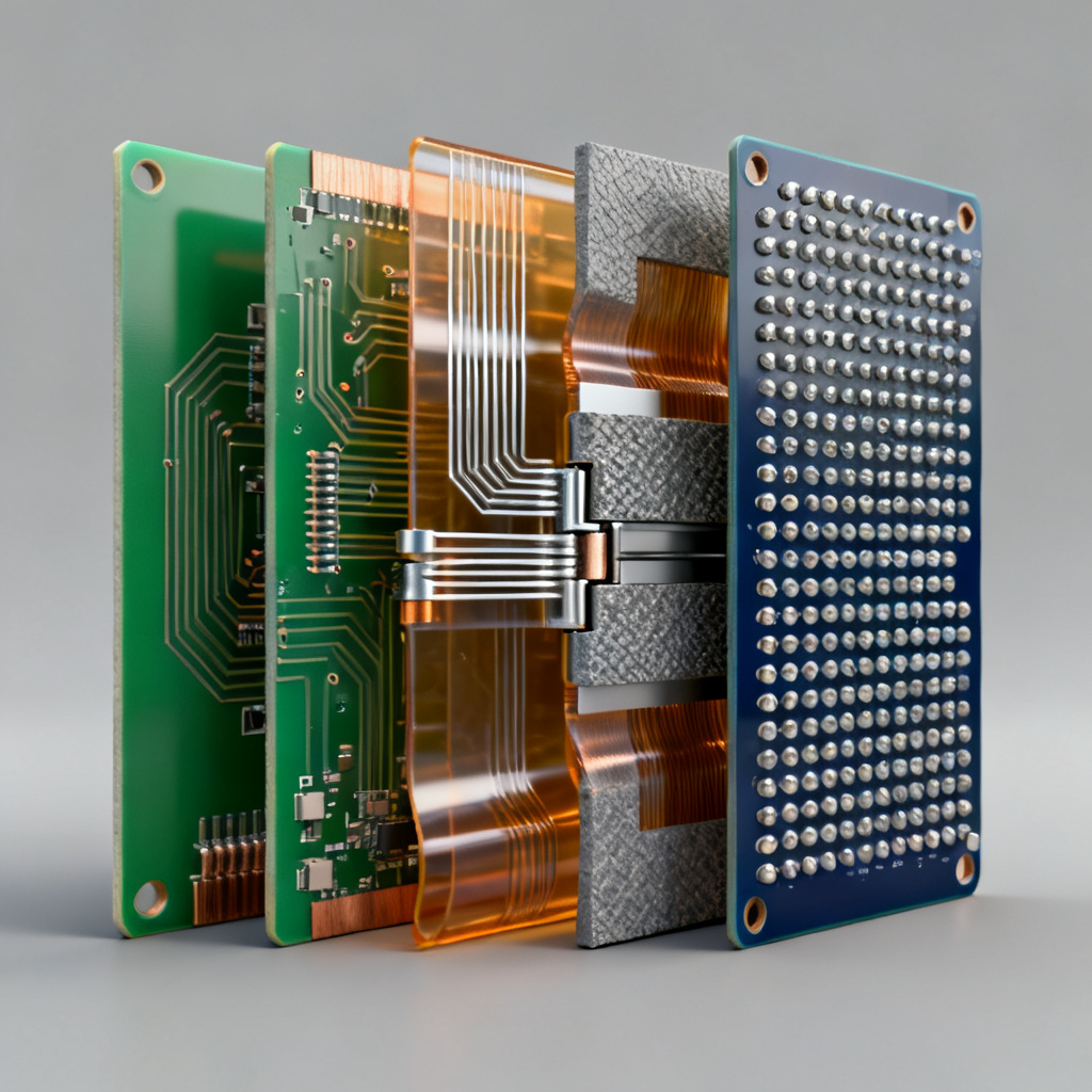
Part 1: Rigid vs Flex vs Rigid-Flex PCB Comparison
1.1 What is a Rigid PCB?
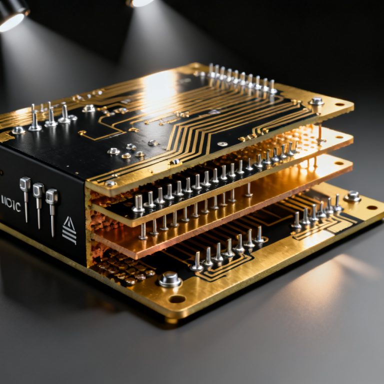
A rigid PCB is the traditional, most common type of circuit board. This PCB type comparison starts with rigid boards constructed on a solid, non-flexible substrate, most commonly FR-4 (a glass-reinforced epoxy laminate), but also on materials like CEM-1, CEM-3, or high-frequency laminates (e.g., Rogers, Teflon). The board has a fixed shape and cannot be bent or twisted.
Key Characteristics:
- Structure: Solid, rigid base material with copper traces laminated on one or both sides.
- Durability: High mechanical strength; provides excellent support for components.
- Cost: Generally the lowest cost per unit for moderate-to-high volumes.
- Applications: Desktop computers, servers, power supplies, industrial controls, automotive ECUs, consumer electronics (TVs, routers).
Advantages:
- Low Cost: Simple manufacturing process and readily available materials make them the most economical choice.
- High Reliability: Proven technology with decades of manufacturing data; excellent thermal and mechanical stability.
- High Component Density: Supports complex, multi-layer designs with fine traces and small vias.
- Easy to Assemble & Test: Standardized processes for SMT, through-hole, and automated optical inspection (AOI).
Limitations:
- No Flexibility: Cannot be bent or folded, limiting design in compact, moving, or 3D-shaped enclosures.
- Requires Connectors & Cables: To connect different rigid boards, you need connectors, wires, and cables, which add cost, weight, and potential failure points.
1.2 What is a Flex PCB?
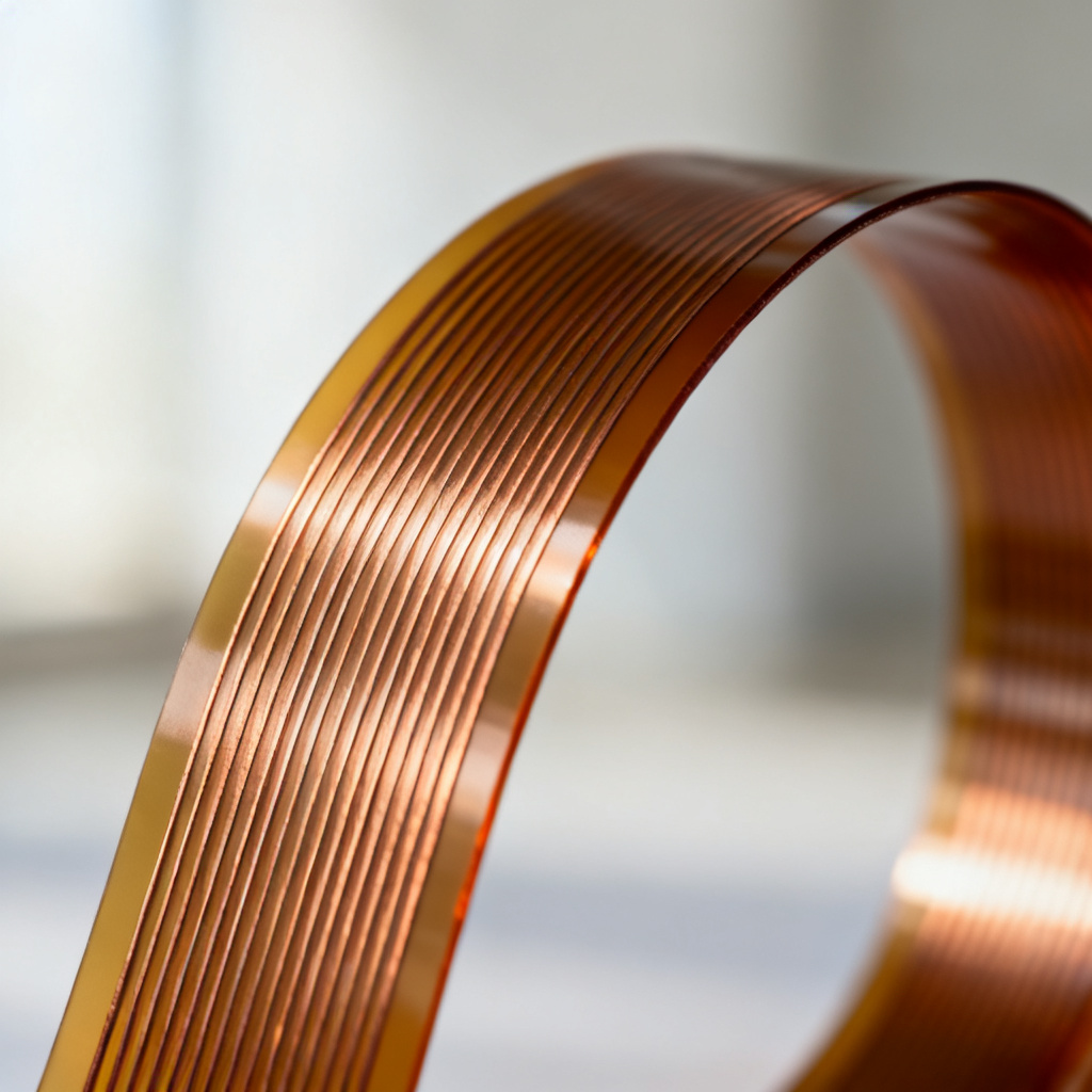
A flex PCB is a circuit board made from flexible plastic substrates, most commonly polyimide (Kapton) or polyester (PET). In this PCB type comparison, flex boards can be bent, twisted, folded, and formed into complex shapes. The copper traces are bonded to the flexible dielectric material, often with a protective coverlay.
Key Characteristics:
- Structure: Thin, flexible dielectric film with etched copper circuits; typically single-sided, double-sided, or multi-layer (limited layers).
- Durability: Excellent dynamic flex life (can withstand millions of bending cycles if designed correctly).
- Cost: Higher per-unit cost than rigid PCBs, especially for low volumes.
- Applications: Smartphones (camera modules, display connectors), medical devices (pacemakers, hearing aids), hard disk drives, printers, wearable electronics, automotive (steering wheel controls, sensors).
Advantages:
- Space & Weight Savings: Eliminates connectors, cables, and wiring harnesses, reducing overall product size and weight by up to 60-70%.
- Dynamic Flexibility: Can be used in applications requiring continuous movement (e.g., printer heads, robotic arms).
- Improved Reliability: Fewer solder joints and connectors mean fewer potential failure points.
- 3D Packaging: Can be bent to fit into tight, irregularly shaped enclosures.
Limitations:
- Higher Material & Tooling Cost: Polyimide and specialized processing are more expensive than FR-4.
- Lower Component Support: Thin, flexible boards offer less mechanical support for heavy components; stiffeners (FR-4 or metal) are often needed.
- Complex Assembly: Handling during soldering is more delicate; requires specialized fixtures.
- Limited Layer Counts: High-layer-count flex PCBs are challenging and costly to manufacture.
1.3 What is a Rigid-Flex PCB?
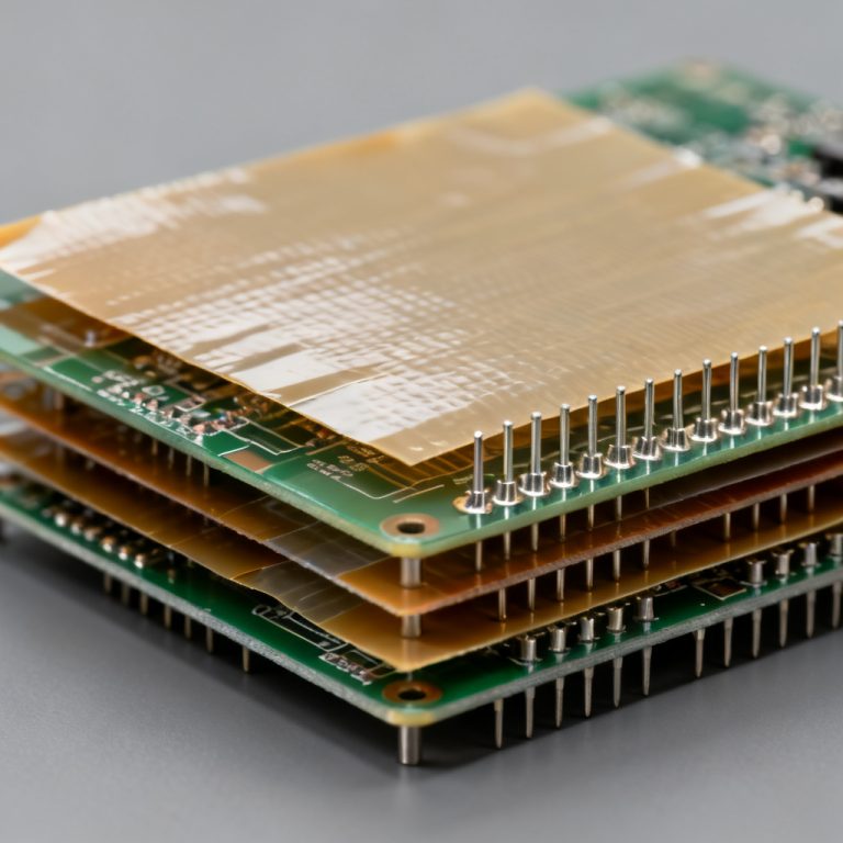
A rigid-flex PCB is a hybrid board that combines rigid (FR-4) and flexible (polyimide) layers into a single, interconnected structure. This PCB type comparison highlights how rigid sections provide mechanical support for components, while flexible sections act as interconnections, eliminating connectors and cables.
Key Characteristics:
- Structure: A “sandwich” of pre-bonded rigid and flexible layers, manufactured as a single unit. The flex layers extend out from the rigid sections.
- Durability: Extremely robust for static bending applications; dynamic flex life depends on design.
- Cost: The most expensive PCB type due to complex design, specialized lamination, and high scrap rates.
- Applications: Aerospace (avionics, satellites), military (radar, communications), medical (implantable devices, surgical tools), high-end consumer (foldable phones, DSLR cameras), industrial (robotics, test equipment).
Advantages:
- Ultimate Space & Weight Savings: Combines the benefits of both rigid and flex; ideal for the most compact, lightweight designs.
- Maximum Reliability: Eliminates the most common failure points—connectors and solder joints between boards.
- Simplified Assembly: A single rigid-flex board replaces multiple rigid boards, cables, and connectors, reducing assembly time and cost.
- Improved Signal Integrity: Continuous copper traces through the flex-to-rigid transition reduce impedance mismatches and signal loss.
Limitations:
- Highest Cost: Design, tooling, and manufacturing are significantly more expensive than rigid or flex alone.
- Complex Design: Requires specialized CAD tools and experienced engineers to manage layer transitions, bend radii, and material stack-ups.
- Longer Lead Times: Manufacturing is slower due to the multiple lamination cycles and complex processing.
- Difficult Rework & Repair: Defects are often impossible to repair; the entire board may be scrapped.
1.4 Head-to-Head Comparison: Rigid vs Flex vs Rigid-Flex
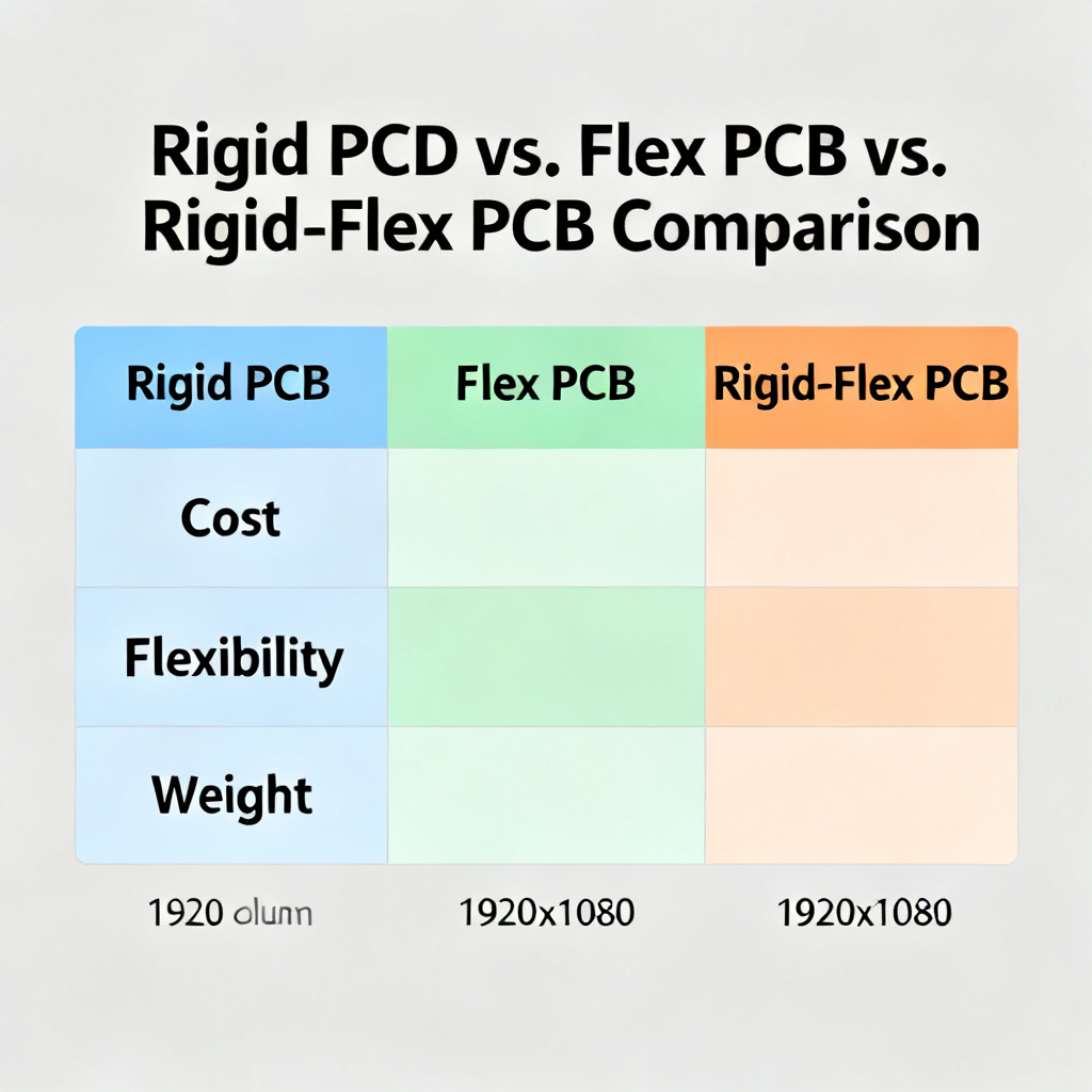
| PCB Type Comparison Feature | Rigid PCB | Flex PCB | Rigid-Flex PCB |
|---|---|---|---|
| Cost (per unit) | Low | Medium-High | High |
| Mechanical Strength | High | Low (needs stiffeners) | High (in rigid areas) |
| Flexibility | None | Excellent (dynamic or static) | Excellent (flex sections) |
| Space & Weight Savings | Poor | Excellent | Maximum |
| Component Density | High | Low-Medium | High (in rigid areas) |
| Reliability (solder joints) | Good | Excellent (fewer joints) | Best (fewest joints) |
| Design Complexity | Low | Medium | High |
| Dynamic Flex Life | N/A | Excellent (if designed for it) | Good (static or limited dynamic) |
| Typical Applications | Consumer, Industrial, Automotive | Mobile, Medical, Wearables | Aerospace, Military, High-end Medical |
Part 2: HDI vs Standard PCB Comparison
2.1 What is a Standard PCB?
A “standard” PCB typically refers to a board manufactured using conventional drilling and lamination processes. In this PCB type comparison, the defining characteristic is that all vias (holes that connect layers) are mechanically drilled. The minimum via size is usually limited by the drill bit diameter (typically >0.2mm / 8 mil). Standard PCBs can be single-sided, double-sided, or multi-layer (up to 20+ layers).
Key Characteristics:
- Via Formation: Mechanically drilled through-hole vias (PTH) and blind/buried vias (if used, they are also mechanically drilled and require sequential lamination).
- Line/Space (L/S): Typically >= 0.1mm / 0.1mm (4 mil / 4 mil) for standard production.
- Cost: Low to moderate, depending on layer count and size.
- Applications: Power supplies, motor drives, industrial controls, basic consumer electronics, automotive body controllers.
Advantages:
- Lowest Cost: Mature, high-volume manufacturing processes keep costs down.
- Simple Design Rules: Easier for engineers to design and layout.
- Wide Material Choice: Compatible with most standard laminates (FR-4, CEM, etc.).
Limitations:
- Larger Vias: Mechanically drilled vias take up valuable real estate on outer layers, limiting routing density.
- Limited Routing Density: Larger vias and wider traces make it difficult to route fine-pitch BGA packages (e.g., 0.5mm pitch or smaller).
- Thicker Dielectric Layers: Standard prepregs are thicker, which can make it harder to achieve controlled impedance in thin boards.
2.2 What is an HDI PCB?
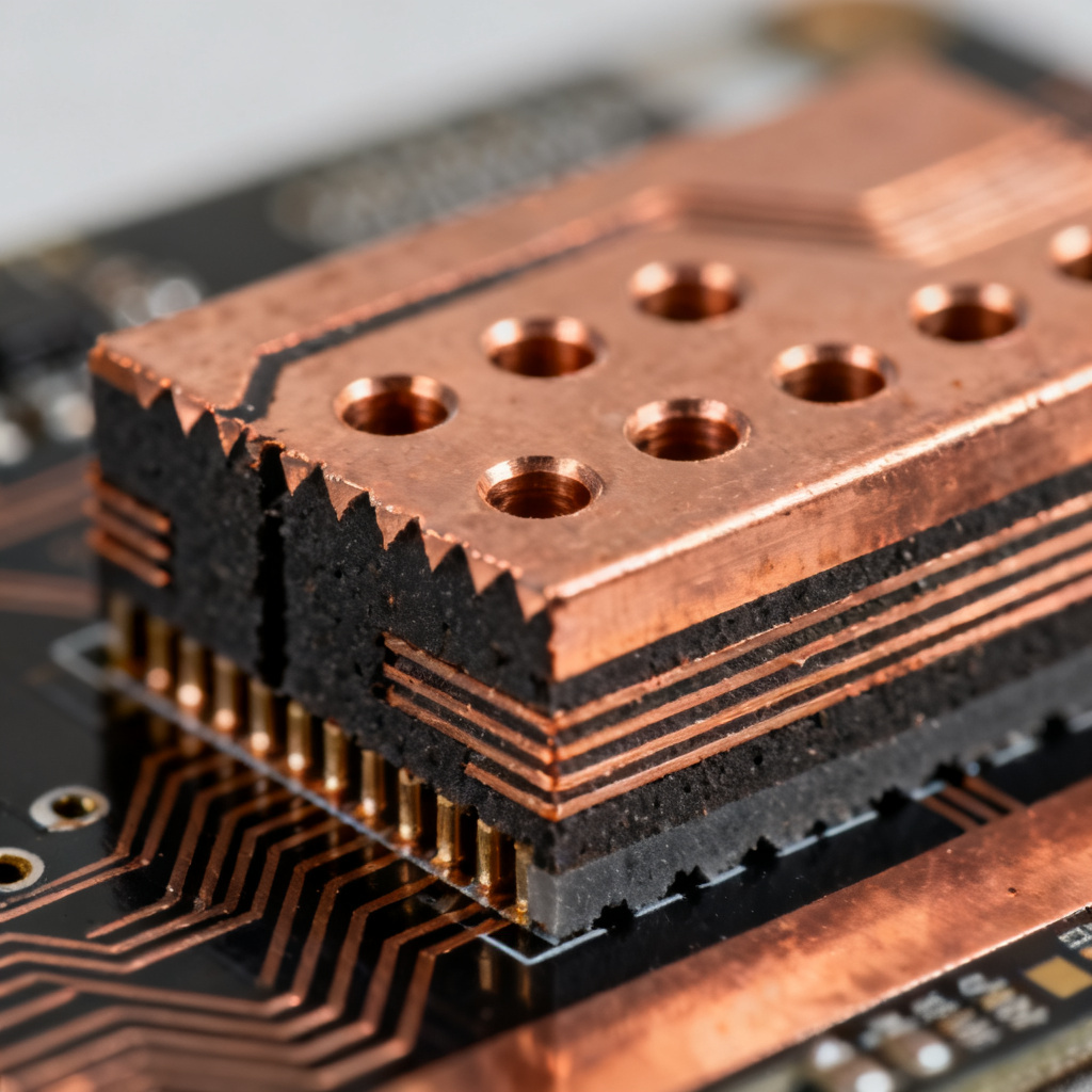
HDI stands for High-Density Interconnect. HDI PCBs are defined by the use of laser-drilled microvias (typically <0.15mm / 6 mil in diameter) instead of mechanically drilled vias. This PCB type comparison emphasizes how microvias allow for much higher routing density, finer line/space geometries, and smaller pad sizes. They are typically built using a sequential lamination process.
Key Characteristics:
- Via Formation: Laser-drilled microvias (blind, buried, and stacked/staggered via-in-pad).
- Line/Space (L/S): Can achieve extremely fine geometries, down to 0.04mm / 0.04mm (1.6 mil / 1.6 mil) or less.
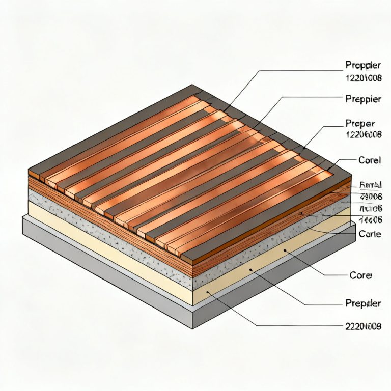
- Layer Count: Often uses “build-up” layers (e.g., 1+N+1, 2+N+2) where N is the core layer count and the “1” or “2” are HDI build-up layers.
- Cost: Higher than standard PCBs due to complex processing, multiple lamination cycles, and specialized equipment.
Advantages:
- High Routing Density: Microvias save significant space, allowing for more routing channels and smaller board sizes.
- Fine-Pitch Component Support: Essential for routing modern BGAs with 0.4mm, 0.3mm, or smaller pitch.
- Improved Signal Integrity: Shorter via stubs and smaller via pads reduce parasitic capacitance and inductance, improving high-speed signal performance.
- Better Thermal Management: Via-in-pad technology allows vias to be placed directly under components for superior heat dissipation.
- Reduced Board Size & Layer Count: In many cases, an HDI design can achieve the same functionality in a smaller size or with fewer layers than a standard PCB.
Limitations:
- Higher Cost: More expensive per square inch than standard PCBs.
- Complex Design & Manufacturing: Requires specialized design rules and high-precision manufacturing equipment.
- Longer Lead Times: The sequential lamination process is inherently slower.
- Limited Material Choice: Not all materials are compatible with laser drilling and the high temperatures of multiple lamination cycles.
2.3 HDI PCB Architecture Levels (IPC-2315)
The IPC-2315 standard defines several levels of HDI complexity:
- HDI Level 1: One build-up layer on one side of the core (e.g., 1+N+0 or 0+N+1). Uses microvias only on one side.
- HDI Level 2: One build-up layer on both sides of the core (1+N+1). This is the most common HDI type.
- HDI Level 3: Two build-up layers on at least one side of the core (e.g., 2+N+2). Allows for stacked microvias.
- HDI Level 4 & Beyond: Three or more build-up layers on one or both sides. Used for the most demanding, ultra-high-density applications.
2.4 Head-to-Head Comparison: HDI vs Standard PCB
| PCB Type Comparison Feature | Standard PCB | HDI PCB |
|---|---|---|
| Via Type | Mechanically drilled (PTH) | Laser-drilled microvias |
| Min. Via Diameter | >0.2mm (8 mil) | <0.15mm (6 mil), down to 0.05mm (2 mil) |
| Min. Line/Space | >= 0.1mm / 0.1mm (4/4 mil) | <= 0.075mm / 0.075mm (3/3 mil), down to 0.04/0.04mm |
| Routing Density | Low to Moderate | High to Very High |
| Fine-Pitch BGA Support | Difficult (0.5mm pitch limit) | Excellent (0.4mm pitch and below) |
| Signal Performance (High-Speed) | Good (with careful design) | Excellent (shorter stubs, lower parasitics) |
| Thermal Performance | Standard | Excellent (via-in-pad) |
| Cost | Low to Moderate | Moderate to High |
| Design Complexity | Low | High |
| Typical Applications | Power, Industrial, Basic Consumer | Smartphones, Tablets, Networking, Medical, Aerospace |
Part 3: How to Choose the Right PCB Type – A Practical Decision Framework
Choosing between these technologies is not about “good” or “bad”—it’s about matching the PCB type comparison to your product’s specific requirements. Use the following decision tree and criteria:
Step 1: Define Your Mechanical Constraints
- Is the product flat and rigid? → Rigid PCB is the default choice. It is the most cost-effective and reliable solution for static applications.
- Does the product need to bend, fold, or fit into a non-planar shape? → Flex PCB is required. If the bending is dynamic (repetitive), you need a high-quality dynamic flex design.
- Do you have multiple rigid boards that need to be connected in a tight space? → Rigid-Flex PCB is the premium solution. It eliminates connectors, saves space, and increases reliability. Evaluate if the cost premium is justified.
Step 2: Assess Your Component Density & Routing Complexity
- Are you using standard components (e.g., QFP, SOIC, through-hole)? → Standard PCB is likely sufficient.
- Are you using fine-pitch BGAs (0.5mm pitch or smaller), high-pin-count devices, or need to fit a complex circuit in a small area? → HDI PCB is necessary. The microvias and fine-line capabilities of HDI are the only practical way to route these devices.
- Is the design a mix of both? → You may need a Standard PCB with HDI build-up layers (e.g., a 1+N+1 HDI structure). This is a common compromise.
Step 3: Evaluate Performance & Environmental Requirements
- High-speed signals ( > 1 GHz)? → HDI PCB is strongly recommended. Microvias minimize signal reflections and crosstalk. Rigid-Flex can also improve signal integrity by eliminating connectors.
- Extreme temperatures, vibration, or shock? → Rigid-Flex offers the highest reliability by eliminating solder joints. Rigid PCBs with high-Tg materials can also withstand high temperatures.
- High power / heat dissipation? → Standard PCBs with heavy copper (2oz, 3oz, etc.) and thermal vias are effective. HDI with via-in-pad can also provide excellent thermal paths.
Step 4: Analyze Total Cost of Ownership (Not Just Unit Cost)
- Low-Volume, High-Performance Product (e.g., Medical Device, Aerospace): The higher cost of Rigid-Flex or HDI is easily justified by the savings in assembly time, improved reliability, and reduced product size.
- High-Volume, Cost-Sensitive Product (e.g., Consumer Toy, Basic Appliance): Standard Rigid PCB is almost always the best choice. The incremental cost of flex or HDI cannot be absorbed.
- Mid-Volume, Mid-Complexity Product (e.g., Automotive ECU, Industrial Controller): A Standard PCB with careful layout or a low-level HDI (1+N+1) often provides the best value.
Summary Decision Matrix
| Application Scenario | Recommended PCB Type | Key Reason |
|---|---|---|
| Simple, static, low-cost | Standard Rigid | Lowest cost, proven reliability |
| Compact consumer device (smartphone) | HDI + Flex | High density, space savings |
| Mission-critical aerospace system | Rigid-Flex + HDI | Maximum reliability, weight savings |
| Medical implant | Rigid-Flex | Small size, high reliability, biocompatibility |
| High-power motor drive | Standard Rigid (heavy copper) | Excellent thermal management, low cost |
| High-speed networking equipment | HDI (high-layer count) | Superior signal integrity |
Conclusion: The Right PCB for Your Success
There is no single “best” PCB type. The decision between Rigid, Flex, Rigid-Flex, HDI, and Standard is a strategic engineering and business choice. A Standard Rigid PCB remains the workhorse of the industry for its unbeatable cost and reliability. A Flex PCB is the enabler of modern, compact, and mobile designs. A Rigid-Flex design is the gold standard for the most demanding applications. HDI technology is the key to unlocking the full potential of advanced, miniaturized components.
As your trusted PCB manufacturing partner, we have the expertise and manufacturing capabilities to produce all of these technologies. We do not just build boards; we help you select the exact right type for your project. Contact our engineering team today for a free DFM review and a detailed cost comparison tailored to your specific design.
Frequently Asked Questions (FAQ) – PCB Type Comparison
What is the main difference in a PCB type comparison between rigid and flex PCBs?
In a PCB type comparison, rigid PCBs use solid FR-4 material and cannot bend, while flex PCBs use polyimide and can be bent or folded. Rigid boards are cheaper and stronger; flex boards save space and weight.
When should I choose HDI over standard PCB in a PCB type comparison?
Choose HDI over standard in a PCB type comparison when you need fine-pitch BGA routing, higher signal integrity for high-speed designs, or smaller board size. HDI uses microvias for greater density.
Is rigid-flex PCB always better than separate rigid and flex boards?
Rigid-flex is not always better in a PCB type comparison; it is more expensive but offers maximum reliability by eliminating connectors. Use it for mission-critical or space-constrained applications where the cost is justified.
How does cost compare in a PCB type comparison between HDI and standard PCB?
In a PCB type comparison, HDI PCBs cost 20-50% more than standard PCBs due to laser drilling and sequential lamination. However, HDI can reduce overall system cost by shrinking board size and layer count.
What does “via-in-pad” mean in a PCB type comparison for HDI?
Via-in-pad is a feature in HDI technology where microvias are placed directly on component pads. In a PCB type comparison, this improves thermal management and signal integrity, especially for high-speed digital designs.