This comprehensive High Layer Count PCB Guide 20 layers handbook delivers advanced stackup design rules for high-density and aerospace systems. High-Layer Count PCB engineering is critical for 5G, aerospace, and medical systems. This guide covers every aspect of 20+ layer boards, from stack-up to cost optimization.
Layer Stackup Planning |
Material Selection |
Signal Integrity & Impedance |
Power Integrity & Thermal |
Manufacturing Challenges |
Cost Optimization |
FAQ
High-Layer Count PCB Stackup Planning
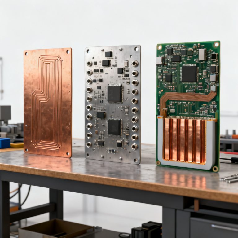
High-Layer Count PCB stackup design directly impacts signal integrity, power integrity, and manufacturability. A symmetrical layer build (e.g., 11+11 for 22 layers) prevents warpage during lamination. Use a mix of cores and prepregs, and plan for sequential lamination cycles (typically 4–6 for 24-layer boards). Dedicate at least two power planes (VCC and GND) adjacent to signal layers to minimize loop inductance. For high-speed signals above 1 GHz, incorporate low-loss dielectrics like Rogers 4350B or Isola IS410, while standard digital domains can use FR-4 (e.g., Isola 370HR). Ensure CTE compatibility when mixing materials.
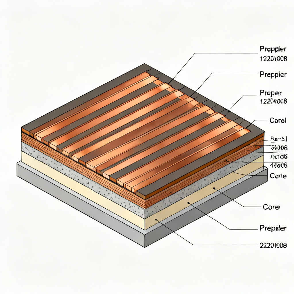
| Layer | Type | Material | Thickness (mil) |
|---|---|---|---|
| 1 (Top) | Signal | Rogers 4350B | 1.2 |
| 2 | GND | FR-4 | 1.0 |
| 3–22 | Signal/Power (alternating) | Hybrid (Rogers + FR-4) | Variable |
| 23 | Power | FR-4 (2 oz Cu) | 2.0 |
| 24 (Bottom) | Signal | Rogers 4350B | 1.2 |
Pro tip: Use copper thieving to balance copper density across layers, reducing thermal stress and warpage.
Material Selection for 20+ Layer PCBs
Choosing the right materials for your High-Layer Count PCB involves balancing electrical performance, thermal stability, and cost. High-Tg FR-4 (Tg 170–180°C) suits moderate thermal demands. Low-loss materials (Rogers, Teflon) are essential for RF/microwave and high-speed digital (e.g., 5G, radar) but cost 3–5x more. Polyimide (Tg >250°C) is used for extreme environments like aerospace. For power layers, consider 2 oz copper (70 µm). Always verify CTE matching between materials to avoid delamination.
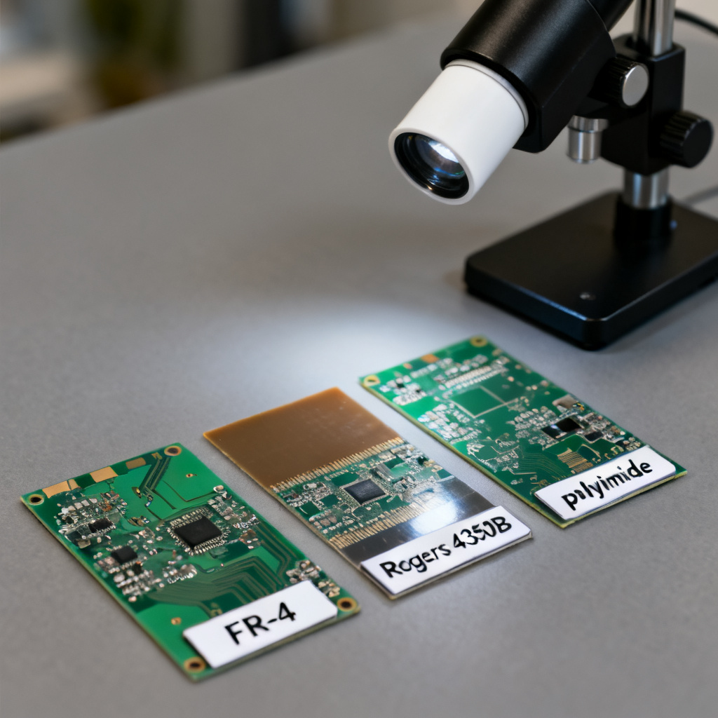
| Material | Tg (°C) | Dk (1 GHz) | Df (1 GHz) | Relative Cost |
|---|---|---|---|---|
| FR-4 (Isola 370HR) | 170 | 4.5 | 0.020 | 1x |
| Rogers 4350B | 280 | 3.48 | 0.0037 | 3–4x |
| Polyimide | >250 | 3.5 | 0.010 | 5x |
Signal Integrity and Impedance Control in High-Layer Count PCBs
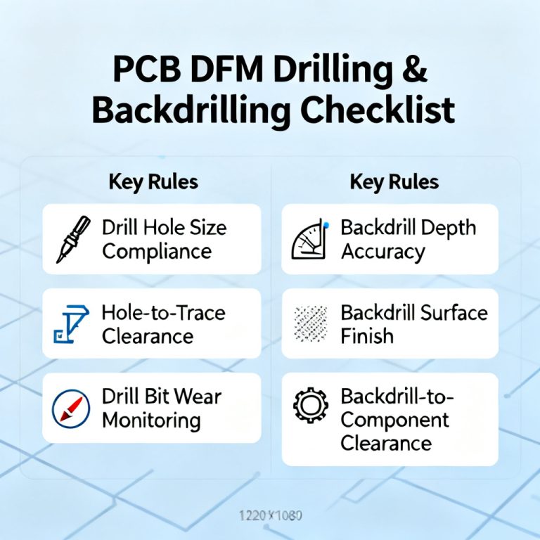
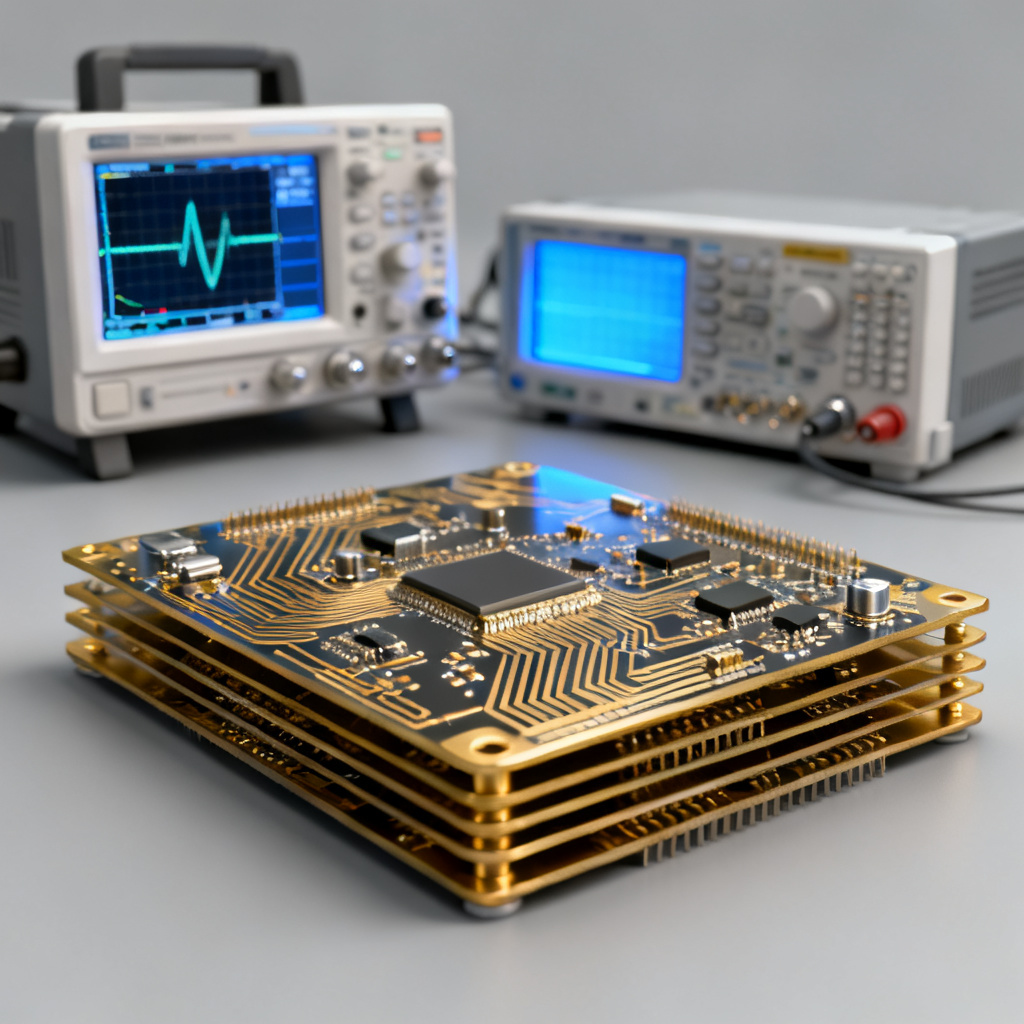
High-Layer Count PCB signal integrity demands precise impedance control (50 Ω single-ended, 100 Ω differential). Use field solvers (e.g., Polar Si9000) to calculate trace width and spacing. For signals above 10 Gbps, back-drilling removes via stubs, reducing reflections. Maintain 3x trace spacing to minimize crosstalk, and use ground stitching vias. Account for ±10% dielectric thickness variation in sequential lamination by specifying a tolerance band (e.g., 50 Ω ± 5%).
Impedance Discontinuity can be mitigated by optimizing via transitions and using microstrip/stripline configurations.
Power Integrity and Thermal Management
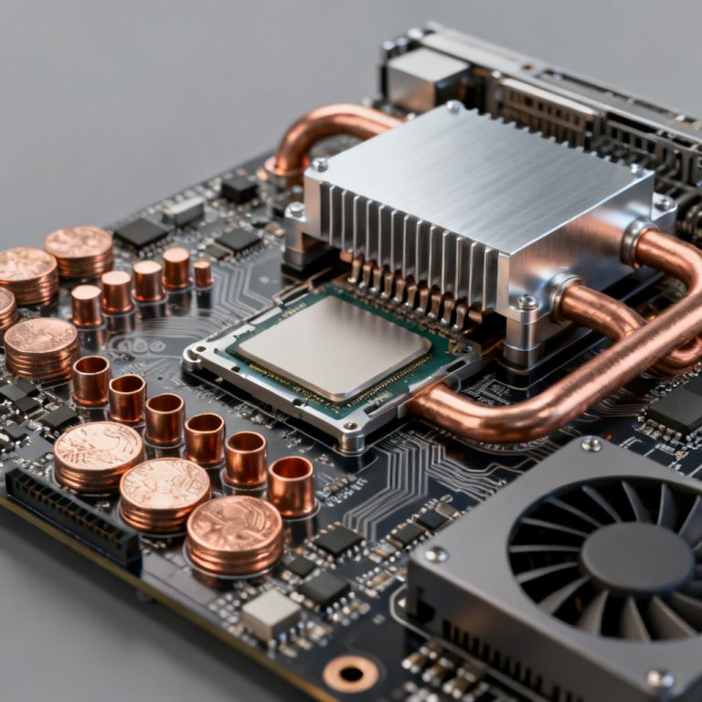
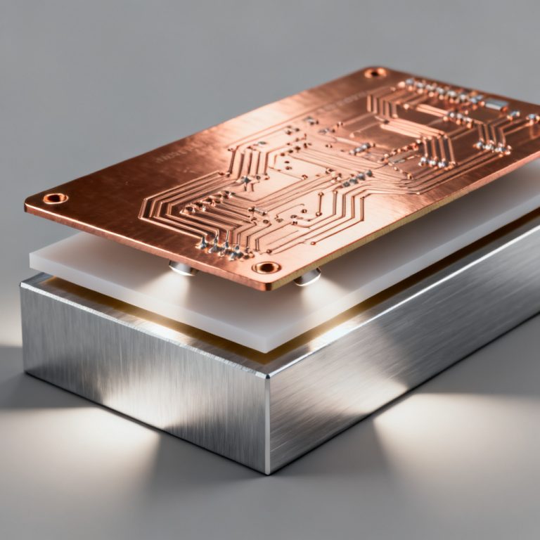
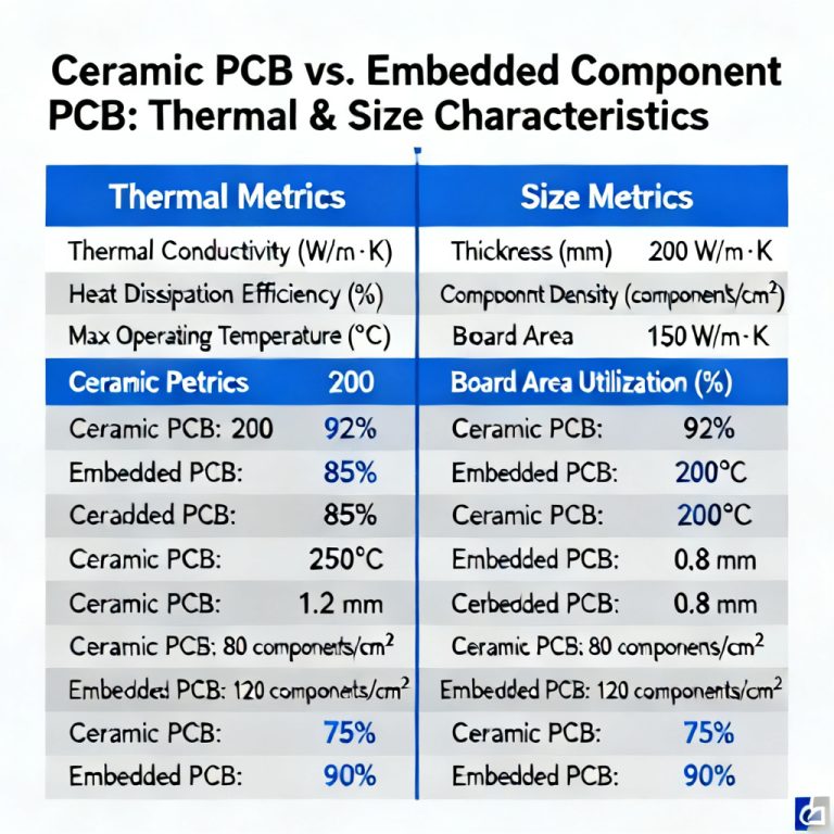
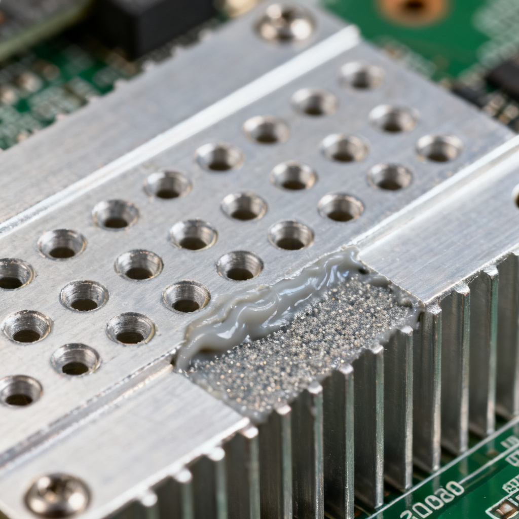
High-Layer Count PCB power integrity relies on embedded capacitance materials (e.g., 3M C-Ply) and decoupling capacitors (0.1 µF + 10 µF) near ICs. For high-power components (FPGAs, processors), use thermal via arrays (0.2–0.3 mm) filled with conductive epoxy. Balance copper density within 20% across all layers to prevent warpage. For boards dissipating >50W, attach aluminum or copper heat sinks with thermal interface materials (TIM).
Manufacturing Challenges for 20+ Layer PCBs
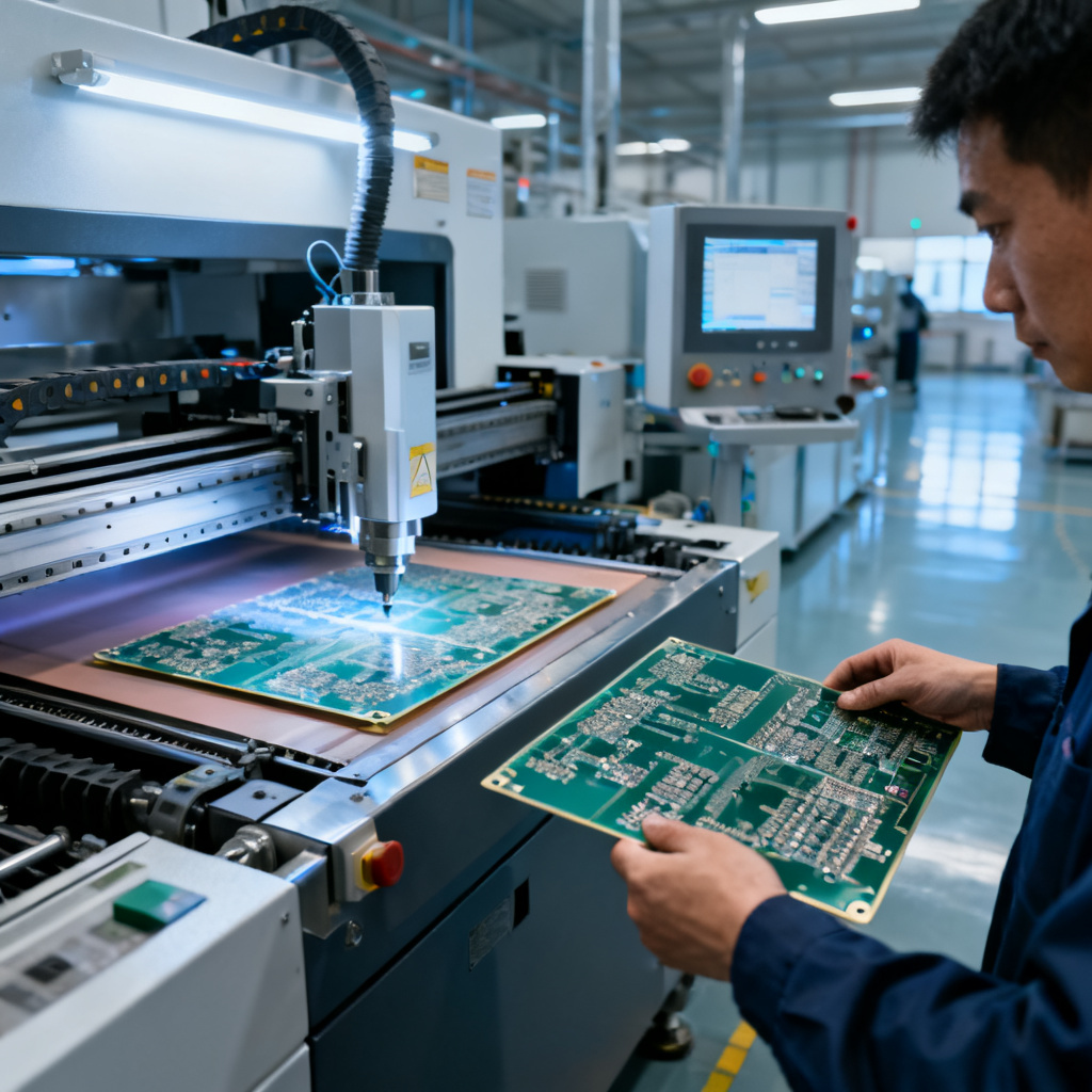
Producing a High-Layer Count PCB involves sequential lamination, tight alignment tolerances (±0.05 mm), and high aspect ratio drilling (max 10:1). Blind/buried vias and microvias (0.1–0.15 mm) require laser drilling. Via filling with conductive epoxy prevents solder wicking. Copper plating must be uniform (25–35 µm in barrel). Use AOI after each lamination cycle and X-ray for inner layer alignment. Impedance testing via TDR and electrical testing (flying probe) ensure quality. Expect yields of 85–95% for 20+ layer boards.
| Parameter | Typical Value | High-End Capability |
|---|---|---|
| Min drill size (mechanical) | 0.2 mm | 0.15 mm |
| Min trace/space | 3/3 mil | 2/2 mil |
| Aspect ratio (through-hole) | 10:1 | 12:1 |
| Copper thickness (outer) | 1 oz | 2 oz |
Cost Optimization for High-Layer Count PCBs
Reduce High-Layer Count PCB cost by minimizing layer count (combine power planes, use high-density routing). Standardize stackup with FR-4 and limit sequential lamination to 2–3 cycles. Optimize panel utilization (standard 18×24 inch) and add copper thieving. Choose a manufacturer with IPC Class 3 certification and negotiate volume discounts for 100+ panels.
Frequently Asked Questions about High-Layer Count PCBs
What is the typical layer count for a High-Layer Count PCB?
Which materials are best for High-Layer Count PCB signal integrity?
How do you control impedance in a 20+ layer PCB?
What are the main manufacturing challenges for High-Layer Count PCBs?
Why Choose Our High-Layer Count PCB Services?
We deliver IPC Class 3 compliant High-Layer Count PCB with 99.5% on-time delivery. Our engineering team provides free DFM review, supports hybrid stackups (Rogers + FR-4), and offers competitive pricing for 20–40 layer boards. Unlike standard vendors, we specialize in sequential lamination with ±0.05 mm alignment and back-drilling for 10+ Gbps signals.