Flexible PCB Guide Single Double Multilayer Flex
Master the Flexible PCB Guide Single Double Multilayer Flex. Understand materials, design rules, stack-ups, manufacturing challenges, and applications. Your ultimate resource for B2B procurement for flexible PCB manufacturing and custom solutions.
1. What is a Flexible PCB?
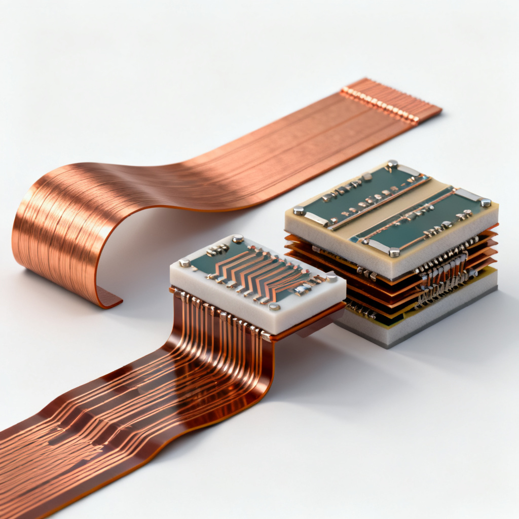
A flexible PCB (Flexible Printed Circuit Board) is a patterned arrangement of printed circuitry and components that utilizes flexible base materials—typically polyimide or polyester films—instead of the rigid fiberglass (FR-4) used in standard boards. The primary advantage of a flexible PCB is the ability to conform to a desired shape during installation or operation, enabling dynamic bending, folding, or static 3D shaping. Flexible PCB designs are not merely “bendable” versions of rigid boards; they are engineered for specific mechanical and electrical performance. They can be single-sided, double-sided, or multilayer, and they often integrate with rigid sections to form rigid-flex assemblies.
2. Single-Layer Flexible PCBs (Single-Sided Flex)
2.1 Definition and Structure
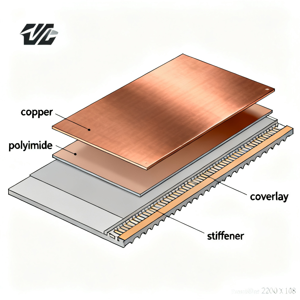
A single-layer flexible PCB consists of a single conductive copper layer laminated onto a flexible dielectric substrate (usually polyimide). The copper is etched to form the circuit pattern. A protective coverlay (also polyimide with adhesive) is applied over the circuitry, leaving pads and termination areas exposed. The back side may have a stiffener (e.g., polyimide, FR-4, or aluminum) for component mounting or connector support.
2.2 Key Characteristics
- Layer Count: 1 copper layer.
- Thickness: Typically 0.1 mm to 0.5 mm (including coverlay and stiffener).
- Flexibility: Highest flexibility among all flex types. Can be dynamically bent millions of times if designed with appropriate bend radius.
- Cost: Lowest cost per unit among flex PCBs.
- Applications: Dynamic applications like printer heads, hard disk drives, camera modules, and simple interconnects in consumer electronics (e.g., cell phone ribbon cables, LCD connectors).
2.3 Design Considerations
For dynamic flexing, the minimum bend radius should be at least 10 times the total thickness of the stack-up (including coverlay and adhesive). For static flex (one-time bend), 6 times thickness is acceptable. Copper weight of 1 oz (35 µm) is standard; 0.5 oz (18 µm) is preferred for extreme dynamic flexing to reduce stress. Use stiffeners only where needed (e.g., under connectors, heavy components). Avoid placing stiffeners in bend areas. Coverlay is mandatory for flex circuits; solder mask is too brittle and will crack under bending.
2.4 Advantages and Limitations
Advantages: Simplest design, fastest prototyping, excellent for high-volume, low-cost interconnects, can be produced with very fine line widths and spaces (down to 0.075 mm / 3 mil). Limitations: No cross-over routing (unless using jumpers or components), limited component mounting area (only one side for components, unless using through-hole).
3. Double-Layer Flexible PCBs (Double-Sided Flex)
3.1 Definition and Structure
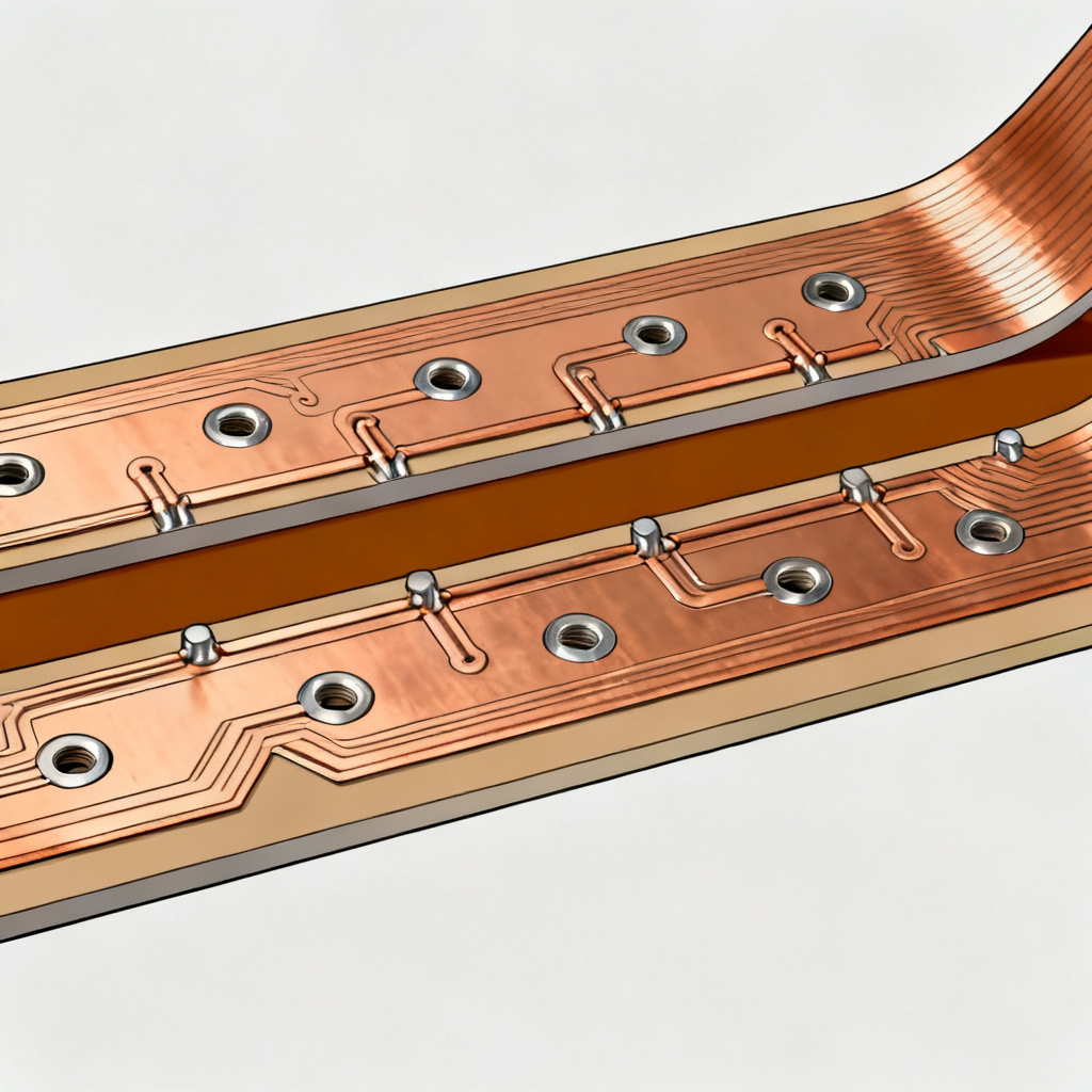
Double-layer flexible PCB have two conductive copper layers separated by a flexible dielectric core (typically polyimide). The two layers are connected by plated through-holes (PTH) or vias. The structure is: Coverlay – Top Copper – Adhesive – Polyimide Core – Adhesive – Bottom Copper – Coverlay. Stiffeners can be added to either side or both sides.
3.2 Key Characteristics
- Layer Count: 2 copper layers.
- Thickness: 0.2 mm to 0.8 mm (without stiffeners).
- Flexibility: Less flexible than single-layer due to the additional copper and dielectric. Still capable of dynamic bending if bend radius is generous.
- Cost: Moderate; more expensive than single-layer but cheaper than multilayer.
- Applications: More complex interconnects requiring cross-overs, shielding, or impedance control. Used in medical devices (e.g., hearing aids, catheters), automotive sensors, and industrial control systems.
3.3 Design Considerations
Plated through-hole (PTH) is standard. Blind vias are possible but increase cost. For dynamic flexing, avoid placing vias directly in the bend area; they create stress concentration points. Balance copper density on both sides to minimize warpage (curling) after lamination. Use cross-hatch patterns (e.g., 50% or 70% copper fill) instead of solid copper pour to improve flexibility. Double-layer flex can be designed for controlled impedance (e.g., 50 ohms) using microstrip or stripline configurations. The dielectric constant of polyimide is typically 3.4 to 3.6. For dynamic flex, minimum bend radius should be at least 20 times the total thickness (including coverlay). For static flex, 10 times thickness is acceptable.
3.4 Advantages and Limitations
Advantages: Allows cross-over routing without extra layers, provides shielding (e.g., using a ground plane on one layer), supports surface mount (SMT) components on both sides (if stiffeners are added). Limitations: Reduced flexibility compared to single-layer, higher material and processing costs, more complex design rules for via placement and copper distribution.
4. Multilayer Flexible PCBs (Multilayer Flex)
4.1 Definition and Structure
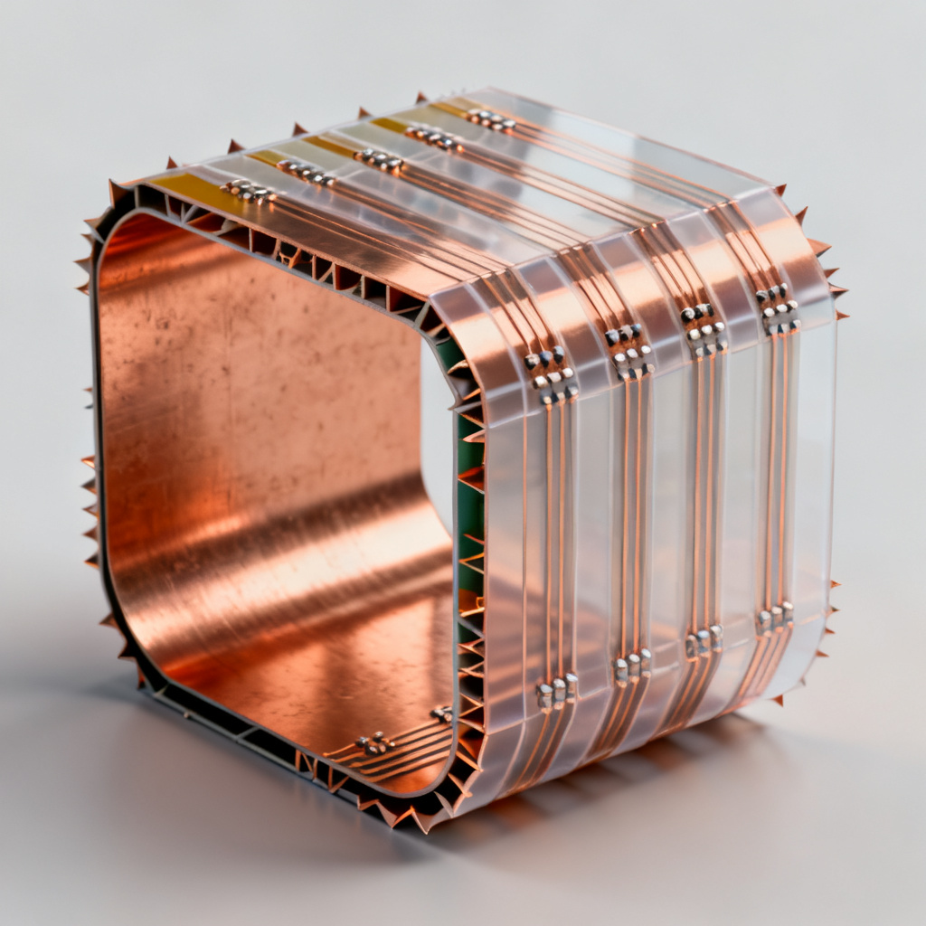
Multilayer flexible PCB consist of three or more conductive copper layers separated by flexible dielectric layers. They are constructed by laminating multiple single-layer or double-layer flex circuits together, with adhesive or prepreg between layers. Vias (PTH, blind, or buried) connect the layers. The entire stack-up is flexible, except where stiffeners are added. Multilayer flex can also be combined with rigid boards to form rigid-flex assemblies.
4.2 Key Characteristics
- Layer Count: 3 to 12+ layers (common range: 4–8 layers for flex; rigid-flex can go higher).
- Thickness: 0.3 mm to 2.0 mm (without stiffeners).
- Flexibility: Limited flexibility; primarily used for static (one-time) bending or moderate dynamic flexing with very generous bend radii.
- Cost: Highest among flex types due to complex lamination and via processing.
- Applications: High-density interconnects in aerospace, military, medical implants, high-end consumer electronics (foldable phones, tablets), and automotive ECUs.
4.3 Design Considerations
For multilayer flex, a symmetrical stack-up (e.g., top copper – core – bottom copper) is critical to prevent warpage during lamination and reflow. Asymmetrical stacks cause curling. As layer count increases, flexibility decreases exponentially. For dynamic flexing, limit to 2–4 layers. For static flex, 6–8 layers are common. Blind and buried vias are often used to save space and reduce layer count. However, they require sequential lamination, which increases cost and lead time. In a rigid-flex design, the flex layers extend from the rigid sections. The transition zone (where rigid meets flex) must be carefully designed with teardrop pads and stress relief slots to avoid tearing. For multilayer flex, minimum bend radius should be at least 30 to 50 times the total thickness (including coverlay). This is because the outer layers experience the most strain.
4.4 Advantages and Limitations
Advantages: Highest circuit density (many layers in a thin, flexible package), excellent for complex routing with multiple power/ground planes, can replace multiple rigid boards and connectors saving space and weight, enables 3D packaging (e.g., foldable phones, wearable devices). Limitations: Very high manufacturing cost, limited dynamic flex capability (mostly static), requires advanced design skills (stack-up, impedance, thermal management), longer lead times (especially for rigid-flex).
5. Materials Used in Flexible PCBs
| Material Type | Common Options | Key Properties | Applications |
|---|---|---|---|
| Dielectric Substrates | Polyimide (PI), Polyester (PET), Liquid Crystal Polymer (LCP) | PI: -200°C to +300°C, excellent chemical resistance; PET: lower cost, up to 105°C; LCP: low dielectric loss, low moisture absorption | PI: standard flex; PET: low-cost consumer; LCP: RF/microwave, aerospace, medical |
| Conductive Foil | Rolled Annealed (RA) Copper, Electrodeposited (ED) Copper | RA: grain structure resists fatigue cracking, preferred for dynamic flex; ED: standard for static flex, lower cost | RA: dynamic flex; ED: static flex |
| Adhesives | Acrylic, Epoxy, No-Flow Prepreg | Acrylic: good flexibility, high peel strength; Epoxy: higher temperature resistance (up to 180°C); No-Flow: prevents resin flow into flex areas | Acrylic: standard flex; Epoxy: high-reliability (military, aerospace); No-Flow: rigid-flex |
| Coverlay vs. Cover Coat | Coverlay (laminated polyimide film), Cover Coat (liquid photoimageable solder mask) | Coverlay: best mechanical protection and flexibility; Cover Coat: cheaper but less flexible | Coverlay: all flex; Cover Coat: static flex only |
6. Manufacturing Process for Flexible PCBs
The manufacturing process for flexible PCB is similar to rigid boards but with critical differences: (1) Material Preparation: Polyimide film with copper cladding is cut to size. (2) Drilling: Mechanical or laser drilling for vias and through-holes; laser drilling preferred for small vias (0.1 mm or less). (3) Plating: Electroless copper plating to make vias conductive, followed by electrolytic copper plating to build up thickness. (4) Etching: Photoresist application, exposure, development, and etching to form the circuit pattern. (5) Coverlay Lamination: Coverlay film is aligned and laminated using heat and pressure; adhesive flows into gaps. (6) Stiffener Lamination: Stiffeners (polyimide, FR-4, or aluminum) are laminated to specific areas using adhesive. (7) Cutting: The flexible circuit is cut from the panel using die-cutting, routing, or laser cutting; laser cutting provides the most precise edges. (8) Electrical Testing: Flying probe or fixture testing for continuity and isolation. (9) Surface Finish: ENIG (Electroless Nickel Immersion Gold) is most common for flex; OSP (Organic Solderability Preservative) is also used for low-cost applications; HASL (Hot Air Solder Leveling) is not recommended due to thermal shock. (10) Final Inspection: Visual inspection and dimensional measurement.
7. Key Design Rules for Flex PCBs
- Avoid 90° corners; use 45° corners or curved traces to reduce stress concentration.
- Always add teardrops to pads and vias in bend areas to prevent lifting.
- No vias or components in the bend area; keepout distance = 2x bend radius.
- For dynamic flex, use 0.5 oz (18 µm) copper; for static flex, 1 oz (35 µm) is acceptable.
- Minimum trace width and spacing: 0.075 mm (3 mil) for standard manufacturing; 0.05 mm (2 mil) is possible with advanced capabilities.
- Minimum annular ring: 0.1 mm (4 mil) for vias; 0.15 mm (6 mil) for component pads.
- For dynamic flex, design the circuit so the neutral axis is at the center of the stack-up to reduce stress on outer copper layers.
- Use stress relief slots at the transition between rigid and flex sections (for rigid-flex).
- Use 50% or 70% copper fill (cross-hatch pattern) instead of solid copper to improve flexibility.
8. Applications Across Industries
| Industry | Application | Type of Flex | Key Requirement |
|---|---|---|---|
| Consumer Electronics | Smartphone ribbon cables, camera modules, foldable displays | Single-layer, double-layer | Dynamic flex, thin profile |
| Medical | Implantable devices (pacemakers), catheters, hearing aids | Multilayer, double-layer | Biocompatibility, high reliability |
| Automotive | Airbag sensors, steering column controls, LED lighting | Double-layer, rigid-flex | Temperature resistance, vibration tolerance |
| Aerospace & Defense | Avionics, satellite communication systems, missile guidance | Multilayer, rigid-flex | High reliability, thermal management |
| Industrial | Robotics, printers, hard disk drives, servo motors | Single-layer, double-layer | Dynamic flex, long cycle life |
| Telecommunications | Base stations, routers, optical transceivers | Multilayer (LCP) | High frequency, low loss |
9. Advantages and Disadvantages Summary
Advantages: Space and weight reduction (eliminates connectors, cables, and harnesses); dynamic flexibility (can withstand millions of bending cycles); 3D packaging (conforms to tight enclosures, enabling smaller products); improved reliability (fewer solder joints and connectors mean fewer failure points); thermal management (polyimide dissipates heat better than some rigid materials). Disadvantages: Higher initial cost (material and tooling costs are higher than rigid PCBs); lower component density (limited by flexibility requirements); handling sensitivity (flex circuits are easily damaged during assembly if not supported); design complexity (requires specialized knowledge for bend radius, stack-up, and material selection).
10. Cost Factors and Considerations for B2B Buyers
When sourcing flexible PCB, the following factors influence cost: layer count (single-layer is cheapest; multilayer and rigid-flex are significantly more expensive); material (polyimide is standard; LCP and specialty materials cost more); copper weight (0.5 oz is slightly cheaper than 1 oz due to less material); stiffeners (adding stiffeners, especially aluminum, increases cost); tolerances (tight tolerances like ±0.05 mm increase scrap rates and cost); volume (high-volume orders of 10,000+ units reduce per-unit cost significantly); surface finish (ENIG is standard; immersion silver or tin are alternatives); testing (full electrical testing adds cost but is essential for high-reliability applications). Recommendation for B2B Buyers: For dynamic flex applications (e.g., moving cables), always specify rolled annealed copper and polyimide coverlay. For static flex (one-time bend), ED copper and cover coat may be acceptable for cost savings. Request a design for manufacturing (DFM) review from your supplier before ordering.
11. How to Choose Between Single, Double, and Multilayer Flex
| Requirement | Recommended Type |
|---|---|
| Simple interconnect, low cost, high volume | Single-layer |
| Need cross-over routing or shielding | Double-layer |
| High circuit density, many signals | Multilayer (4–8 layers) |
| Dynamic bending (millions of cycles) | Single-layer (RA copper) |
| Static bending with complex routing | Multilayer (with generous bend radius) |
| Integration with rigid boards | Rigid-flex (multilayer) |
| High-frequency signals (RF) | Multilayer with LCP material |
12. Common Mistakes to Avoid
- Ignoring bend radius: the most common failure cause; always calculate minimum bend radius based on total stack-up thickness.
- Using solid copper planes in bend areas: causes cracking and delamination; use cross-hatch patterns.
- Placing vias in bend zones: vias act as stress risers; they will crack and break.
- Mixing rigid and flex materials improperly: in rigid-flex, the transition zone must have stress relief slots and teardrops.
- Not specifying coverlay: solder mask will crack; always specify coverlay for flex.
- Overlooking stiffener placement: stiffeners should not extend into bend areas; leave a gap of at least 2 mm.
- Forgetting to balance copper: asymmetrical copper distribution causes warpage during lamination and reflow.
13. Future Trends in Flexible PCB Technology
Ultra-thin flex down to 0.05 mm total thickness for wearable devices; embedded components (passive components like resistors, capacitors embedded inside the flex layers to save space); hybrid materials combining polyimide with LCP for high-frequency + flexibility; additive manufacturing (inkjet printing of conductive traces on flexible substrates for rapid prototyping); stretchable electronics (a new category beyond flexible, allowing stretching and twisting, e.g., for medical skin patches).
14. Conclusion
Flexible PCB are a critical technology for modern electronics, enabling miniaturization, weight reduction, and dynamic movement. Understanding the differences between single-layer, double-layer, and multilayer flex is essential for selecting the right solution for your application. Whether you need a simple ribbon cable for a consumer device or a complex rigid-flex assembly for aerospace, the design rules, material choices, and manufacturing considerations outlined in this guide will help you make an informed decision. For B2B procurement, always work with a manufacturer that offers DFM support, material verification, and rigorous testing. By mastering these fundamentals, you can leverage flexible PCB to create innovative, reliable, and cost-effective products.
15. Frequently Asked Questions (FAQ)
What is a flexible PCB used for?
A flexible PCB is used in applications requiring dynamic bending, space savings, or 3D packaging, such as consumer electronics, medical devices, automotive sensors, and aerospace systems.
How do I choose between single-layer and multilayer flexible PCB?
Choose a single-layer flexible PCB for simple, low-cost interconnects and dynamic bending; choose a multilayer flexible PCB for high circuit density, complex routing, and static bending applications.
What materials are best for a flexible PCB?
Polyimide is the standard material for flexible PCB due to its excellent thermal and mechanical properties; rolled annealed copper is preferred for dynamic flex, while electrodeposited copper is suitable for static flex.
Can a flexible PCB be repaired?
Repairing a flexible PCB is challenging due to its thin and delicate structure; it is often more cost-effective to replace the entire flex circuit rather than repair it.
What is the minimum bend radius for a flexible PCB?
The minimum bend radius for a flexible PCB depends on the layer count and stack-up; for single-layer dynamic flex, it is typically 10 times the total thickness, while for multilayer static flex, it can be 30 to 50 times the total thickness.
16. Glossary of Key Terms
- Coverlay: A protective polyimide film laminated over the circuitry of a flexible PCB to provide insulation and mechanical protection.
- Dynamic Flex: A flexible PCB designed to withstand repeated bending cycles during operation, such as in printer heads or hard disk drives.
- Static Flex: A flexible PCB designed for one-time or infrequent bending during installation, such as in foldable devices or rigid-flex assemblies.
- Stiffener: A rigid material (e.g., polyimide, FR-4, or aluminum) added to a flexible PCB to support component mounting or connector attachment.
- Cross-hatch Pattern: A grid-like copper fill pattern used in flexible PCB to improve flexibility while maintaining electrical performance.